Ultrafast voltage sampling using single-electron wavepackets
N. Johnson, J. D. Fletcher, D. A. Humphreys, P. See, J. P. Griffiths, G. A. C. Jones, I. Farrer, D. A. Ritchie, M. Pepper, T. J. B. M. Janssen, and M. Kataoka
Citation: Appl. Phys. Lett. 110, 102105 (2017); doi: 10.1063/1.4978388
View online: http://dx.doi.org/10.1063/1.4978388
View Table of Contents: http://aip.scitation.org/toc/apl/110/10
Published by the American Institute of Physics
Articles you may be interested in
Visualizing near-field coupling in terahertz dolmens
Appl. Phys. Lett. 110, 101105101105 (2017); 10.1063/1.4978031
Photonic spin Hall effect by the spin-orbit interaction in a metasurface with elliptical nano-structures
Appl. Phys. Lett. 110, 101908101908 (2017); 10.1063/1.4978520
Surface magnetism and proximity effects in hexaboride thin films
Appl. Phys. Lett. 110, 102404102404 (2017); 10.1063/1.4978433
Dual-spacer nanojunctions exhibiting large current-perpendicular-to-plane giant magnetoresistance for ultrahigh density magnetic recording
Appl. Phys. Lett. 110, 102401102401 (2017); 10.1063/1.4977948
Current-induced surface roughness reduction in conducting thin films
Appl. Phys. Lett. 110, 103103103103 (2017); 10.1063/1.4977024
Contact resonance AFM to quantify the in-plane and out-of-plane loss tangents of polymers simultaneously
Ultrafast voltage sampling using single-electron wavepackets
N.Johnson,1,2J. D.Fletcher,1D. A.Humphreys,1P.See,1J. P.Griffiths,3G. A. C.Jones,3 I.Farrer,3,a)D. A.Ritchie,3M.Pepper,2T. J. B. M.Janssen,1and M.Kataoka1,b)
1
National Physical Laboratory, Hampton Road, Teddington, Middlesex TW11 0LW, United Kingdom.
2
London Centre for Nanotechnology, and Department of Electronic and Electrical Engineering, University College London, Torrington Place, London WC1E 7JE, United Kingdom
3
Cavendish Laboratory, University of Cambridge, J.J. Thomson Avenue, Cambridge CB3 0HE, United Kingdom
(Received 27 January 2017; accepted 21 February 2017; published online 9 March 2017)
We demonstrate an ultrafast voltage sampling technique using a stream of electron wavepackets. Electrons are emitted from a single-electron pump and travel through electron waveguides towards a detector potential barrier. Our electrons sample an instantaneous voltage on the gate upon arrival at the detector barrier. Fast sampling is achieved by minimising the duration that the electrons interact with the barrier, which can be made as small as a few picoseconds. The value of the instan-taneous voltage can be determined by varying the gate voltage to match the barrier height to the electron energy, which is used as a stable reference. The test waveform can be reconstructed by shifting the electron arrival time against it. Although we find that the our current system is limited by the experimental line bandwidth to 12–18 GHz, we argue that this method has scope to increase the bandwidth of voltage sampling to 100 GHz and beyond.Published by AIP Publishing.
[http://dx.doi.org/10.1063/1.4978388]
There is much interest in producing faster electronic devices for high-performance computing, large-volume data communication, and quantum technologies. High frequency signal analysis becomes important in the testing and design of these high speed applications. The bandwidth of commer-cial sampling oscilloscopes using sampling gates is approaching 100 GHz.1,2The limiting factor to their band-width is the parasitic capacitance in the components.3While it is in principle straightforward to generate trigger pulses at picosecond length for sampling gates, parasitic loss limits the sampling bandwidth. In addition, there is a need to pro-duce high bandwidth signal processing techniques in the cryogenic environment, as many quantum technology imple-mentations require ultra-low operation temperatures.4,5It is generally difficult to link the conventional room-temperature instruments and quantum devices at low temperatures through high-bandwidth wiring.
A radical approach to these problems may be to use a short wavepacket of a single quasiparticle (e.g., a conduction band electron) instead of a voltage trigger pulse. The infor-mation transmitted by a quasiparticle wavefunction is pro-tected in the absence of scattering or tunneling events. The use of this wavefunction as the media of (classical) informa-tion transfer would allow us to achieve high-speed device operations without the bandwidth limitations imposed by conventional transmission lines.
In this letter, we present an ultrafast voltage sampling method using single-electron wavepackets traveling through electron waveguides in a semiconductor substrate. An unknown test signal is added to a known gate voltage to form a potential barrier in the path of the electron wavepackets.
The transmission probability through the barrier depends on the instantaneous barrier height on arrival at the detector rela-tive to the electron energy. In this manner, our electrons can sample the test signal voltage, in a similar way to the sample and hold method using a voltage comparator in conventional sampling gates3High bandwidth of this sampling is achieved by tuning the electron’s arrival-time distribution (ATD) to 10 ps or shorter.6Our method in principle eliminates the band-width limitation that plagues conventional electronic devices. While we are presently limited by the bandwidth of the trans-mission line of the test signal, we argue that this method has the potential to increase the bandwidth of voltage sampling up to 100 GHz and beyond.7
The principle of our single-electron-sampling (SES) scheme is presented in Figs.1(a)–1(c). Single-electron wave-packets are generated at a fixed energy and travel along the same path towards a potential barrier, which we call the detector barrier. The direction the wavepackets travel on arrival at the detector barrier depends on the barrier height, which is controlled by a gate voltage. If the electrons have an energy greater than the potential on this barrier, they pass through it, otherwise they are deflected. This path direction is only dependent on the instantaneous barrier potential at the time of electron arrival. Therefore, we can use this infor-mation to sample the voltage at a very short timescale.
We initially apply a detector gate voltage such that the barrier is held at half transmission [Fig. 1(a)]. At this volt-age, each electron has a 50% probability of tunneling through the detector potential. We denote this threshold volt-age as the “Reference.” When we add a test signal to the detector gate, the transmission of wavepackets either increases or decreases, depending on the sign of the test sig-nal [Fig.1(b)(i) and (ii)]. We then add a further dc voltage to the detector gate, which we call the “Offset” [Fig.1(c)]. If the magnitude of the Offset matches that of the instantaneous
a)Present address: Department of Electronic and Electrical Engineering,
University of Sheffield, Mappin Street, Sheffield S1 3JD, United Kingdom
b)
test signal, but with the opposite sign, then the barrier is brought back to the original point of half transmission. This way, we can “sample” the instantaneous value of the test signal.
The SES method can be compared to that of voltage sampling by a sample and hold method3,8 as shown in the simplified block diagrams in Fig. 1(d). In the sample and hold method, a trigger pulse closes a switch which permits the test signal to propagate onto a capacitor. When the switch is opened, the voltage is fed into a comparator for analog-to-digital conversion. This allows a fast waveform to be sam-pled by the capacitor taking “snapshots” of the waveform each time it is charged. In the SES method, single-electron wavepackets represent trigger pulses. The voltage compari-son is made between the test signal and Offset voltage (with opposite signs), and the result is read by the direction that our electrons travel. The waveform of the test signal can be scanned by shifting the electron arrival time against it to sample different parts of the waveform. In principle, this method should work in a single-shot mode (for real-time sampling), in which we could use a charge sensor to record the transmission of a single electron across the detector bar-rier. Although technologically plausible, we do not yet have
such capability. Scaling to full waveform resolution in single shot mode requires the use of multiple electron pumps.9 Here, as a demonstration of proof of principle, we use a peri-odic test signal, to which the timing of electron wavepacket emission is synchronised. Hence, the direction of electron flow can be detected as a current.
Fig.1(e) shows a schematic of the device and connec-tions used to realise the SES scheme. A GaAs/AlGaAs heter-ostructure defines a two dimensional electron gas (2DEG)
90 nm below the surface. The active area of the device is etched to confine the 2DEG to a 1.5lm-wide channel (grey shading). Ti/Au gates G1, G2, and GD are patterned on the
surface. Gates G1 and G2 define the single-electron
pump,10–12 which is our source of electron wavepack-ets.6,13–15 Gate GD forms the detector barrier 4lm away
from the pump. Experiments are performed in a cryostat with a base temperature300 mK and with a perpendicular magnetic field ofB¼14 T.16
The electron pump is operated so that it emits electrons one by one at a stable fixed energy 100 meV above the Fermi energy, with a typical broadening 4 meV [the full width at half maximum (FWHM)].14G1is driven by an ac
sinusoidal waveform VAC
G1 at 240 MHz with peak-to-peak
amplitude 1 V from one channel of an arbitrary waveform generator (AWG).17During the pump cycle, an electron pop-ulates the quantum dot, and is then ejected over the drain barrier G2. This produces a quantised current I¼ef, with e
the elementary charge and f the frequency of the driving waveform. In the presence of a sufficiently large B, the ejected electrons travel along the sample edge [marked as red paths in Fig. 1(e)] as in the edge-state transport in the quantum Hall regime,18 but as hot electrons in the states higher than the Fermi energy. No appreciable energy loss occurs between the pump and the detector due to a long scat-tering length of order of tens of microns.14,15,19,20
A test signalVGDAC is applied to the detector from the
sec-ond channel of the AWG, synchronised to the pump signal
FIG. 1. (a)–(c) Principle of the single-electron-sampling (SES) scheme. (a) We find the gate voltage (Reference) that gives half transmission through the barrier for incoming electron wavepackets. (b) When we add an unknown test signal transmission is modified to either (i) fully reflected or (ii) fully transmitted because the total potential on the gate is modified. (c) By adding the Offset voltage we return the detector gate potential to the half transmission point. (d) Block diagram comparisons between a sample-and-hold method and our SES method. (e) Schematic of the experimental setup. Gates G1 and G2 form the electron pump, which produces single-electron
wavepackets. These propagate across the device in edge states (red) to the detector barrier GD, which implements the SES scheme presented in (a)–(c).
FIG. 2. (a) Changing the time delay,Dtd, allows the electron wavepacket to sample different parts of the test waveform. The sampling window is propor-tional to the length of the wavepacket in the time domain. (b) The derivative dID=dDVGDDCplotted againstVGDDCandDtd, which indicates the electron trans-mission threshold. The detector currentID¼0 below this threshold (more negativeVDC
GDwhileIDefabove the threshold. (c) Filled squares show the peak centre of a Gaussian fit to the experimental data in (b). The red curve is a sine fit to the peak centre. Inset: The residual of the fit, implying good line-arity at this voltage scale.
[image:3.612.54.298.54.362.2] [image:3.612.317.560.514.676.2](for this work, we use a two-channel Tektronix AWG7122C, but in principle any synchronised RF source could be used). The pump drive signal, and, for this first test, the detector test signal, are filtered using a 630 MHz low pass filter. We place an ammeter on the ohmic contact behind the detector [see Fig.1(e)] so that it records the detector transmission as the transmitted current ID. We set the Reference, VDCGD and
OffsetDVGDDCvoltages on the detector gate as shown in Figs. 1(a)–1(c). We track the half transmission point by adjusting the Offset, and deduce the instantaneous voltage of the test waveform.
Fig.2(a)shows how we sample the test waveform at dif-ferent times to build up its temporal form. Changing the delay betweenVGAC1 andV
AC
GD by a quantity Dtd allows us to
control the arrival time of the electrons at the detector. Electrons will then sample a different part of the test wave-form. We can control Dtd with 1 ps resolution, using the
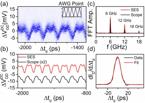
internal skew control between the two output channels of the AWG. Because the electron arrival time distribution (ATD) is so short compared to the timescale that our test waveform voltage changes, we consider the waveform to be quasi-static during the sampling time.
Fig. 2(b)is an example result, with a filtered 240 MHz sine wave as the test waveform21plotting in the colour scale, the derivative dID=dDVGDDC of the measured current with
respect to the Offset voltage. The vertical axis is the Offset
DVGDDC, and the horizontal axis isDtd. We perform a Gaussian
peak fit to this derivative and plot its peak centre as a filled square in Fig.2(c).22 The derivative represents the detector arrival energy distribution, and its peak centre is a good mea-sure of the electron mean energy (although, strictly speaking, this may not be exactly the case, as the actual energy distri-bution may not be a symmetric function14,23). Inverting the sign on the DVGDDC-scale gives the measured waveform. To
examine the linearity of this method, we fit a sine curve (red line) to the experimental data points in Fig.2(c). The resid-ual of the fit is plotted in the inset to Fig.2(c). The standard deviation of the residual is 160lV, and suggests that this method has a good linearity at this level (our dc gate voltage source, a Keithley 213, has an accuracy of 1 mV).
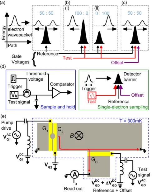
The results mentioned above demonstrate the basic prin-ciple of the SES method. We now explore its bandwidth lim-itation. We remove the filter from the test-signal line, so that the distortion by higher harmonics from the AWG transmits to the detector gate. The AWG construction of a sine wave is shown in Fig.3(a), and the resultant current map in Fig.3(b), again plotted with the derivative of current in the colourscale for clarity, as in Fig.2(b). Again, we extract the derivative-peak positions and plot them in Fig.3(c)(red curve). There are high-frequency distortions clearly visible, dominated by 12 GHz components at the AWG’s sampling rate.
To compare these results against the conventional sam-pling method, we connect a Tektronix MSO72304DX Mixed Signal Oscilloscope (analog bandwidth 23 GHz) at the end of the measurement probe instead of our sample holder con-taining the device (at room temperature).24We measure the AWG signal by the oscilloscope through the same signal line as the detector. In Fig. 3(c), we compare the oscilloscope trace (black curve) with the SES result. Because the oscillo-scope measurement (50Xtermination) has an amplitude of
approximately half the magnitude of the SES scheme (open ended), we scale the scope trace by a factor of 2 to make it easier to compare the traces. We also inverted the sign of the voltage for the oscilloscope trace, as the SES trace is inverted when plotted in the Offset voltage. While the over-all features are similar, the SES trace shows stronger, higher harmonic signal. In Figs.3(d)–3(f), we repeat the same anal-ysis for a 240 MHz unfiltered square wave. Again, the higher harmonic features are stronger for the SES trace.
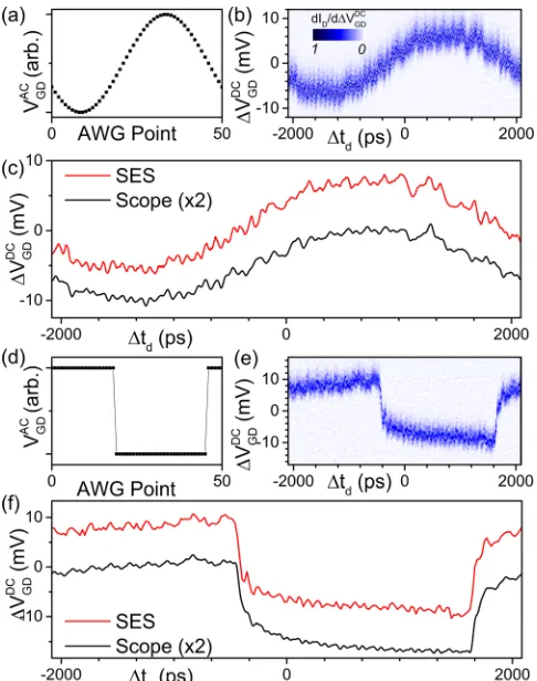
In order to investigate the high-frequency response of the SES system further, we use the two-point waveform con-struction to generate highest-frequency oscillations (6 GHz) as shown in the inset to Fig.4(a) (the single-electron pump frequency is kept at 240 MHz). We obtain the current mea-surement map in Fig.4(a), and plot the peak-position extrac-tion (red curve) and oscilloscope trace (black curve) in Fig.
4(b). They show slightly differing waveform shapes, proba-bly due to a small phase difference affecting the higher fre-quency components. We take the Fast Fourier Transform (FFT) amplitude of both traces, and plot them in Fig. 4(c). The SES trace records the 12 GHz component almost twice as high as that of the oscilloscope trace, while the latter records the 18 GHz component which is not seen on the for-mer trace.
We estimate that the SES method should have a band-width well in excess of 18 GHz. The arrival-time distribution
[image:4.612.317.560.52.360.2](ATD)6 of the electrons measured at the detector barrier is 14 ps (FWHM) as shown in Fig. 4(d). This should give a temporal resolution of 28 ps, corresponding to a bandwidth of 35 GHz. We speculate that the lack of 18 GHz peak in the SES FFT in Fig.4(c)may be due to the bandwidth limitation of the transmission line on our sample holder and GaAs chip. The results in Figs.3and4imply that the SES method has a higher bandwidth at 12 GHz. However, the oscilloscope used should have a flat passband up to 11.5 GHz. Since it is unlikely that our bandwidth can be better, we speculate that the excess amplitude at 12 GHz may be due to an unidenti-fied non-linear effect, although we do not see such an effect in the lower-frequency data [Fig.2(c)]. Further studies are needed to clarify the bandwidth performance of the SES method. Recent work on the temporal wavepacket size indi-cates that with careful tuning of the ATD via tuning of the pump operating conditions,6,14,23 it is plausible to generate wavepackets with ATD less than 10 ps, and has theoretically been shown to be tunable to 1 ps.25This is because the ATD is determined by the time taken for the pumped electron to tunnel across the barrier G2. Hence, this opens the possibility
of a bandwidth in excess of 100 GHz if the bandwidth of the detector transmission line can be improved, and the transmis-sion function made sharper in time. Dispertransmis-sion and distortion of the wavepacket during propagation from pump to detector can be considered negligible with an ATD size of 14 ps and short path length.15,20
To summarise, we have demonstrated a technique of using single-electron wavepackets to sample an unknown test waveform. This method is analogous to that employed in a sampling oscilloscope, but with the possibility of realising a bandwidth in excess of 100 GHz. Other than high-bandwidth applications, one area in which this method can be useful is in-situ voltage waveform measurements in a cryogenic environment. On-chip signal verification is becoming increasingly important for fine control of quantum systems, for example, in qubit state initialisation.26
Our system might be useful in such applications, as a way of verifying the shape of signals on chip, and opens up the possi-bility of quantum measurements through precise signal control.
We thank J. Marrinan, C. Skach, and J. Niblock from Tektronix for useful discussions on AWG and sampling oscilloscope technologies. We also thank S. P. Giblin for useful discussions. This research was supported by the UK Department for Business, Energy, and Industrial Strategy and by the UK EPSRC.
1
Tektronix, Techniques for Extending Real-Time Oscilloscope Bandwidth (Tektronix, 2016).
2Keysight Technologies, What Is the Difference between an Equivalent
Time Sampling Oscilloscope and a Real-Time Oscilloscope? (Application Note)(Agilent, 2013).
3
T. H. O’Dell, Circuits for Electronic Instrumentation (Cambridge University Press, 1991).
4Scalable Quantum Computers: Paving the Way to Realization, edited by
S. Braunstein, H.-K. Lo, and P. Kok (Wiley and Sons, 2005).
5H. M. Wiseman and G. J. Milburn,Quantum Measurement and Control
(Cambridge University Press, 2011).
6
J. Waldie, P. See, V. Kashcheyevs, J. Griffiths, I. Farrer, G. Jones, D. Ritchie, T. Janssen, and M. Kataoka,Phys. Rev. B92, 125305 (2015).
7
For this work, we focus on demonstrating our method in the conventional mK cryogenic environment, but we anticipate that the method would work in the 4 K liquid He environment, with a field as low as 5 T.
8
J. M. D. Pereira,IEEE Instrum. Meas. Mag.9, 27 (2006).
9We note that the type of electron pump used here has been demonstrated
to have accuracy at the part per million level.12At this level of accuracy, we speculate that the single charge detection method will be the limiting accuracy factor.
10
M. D. Blumenthal, B. Kaestner, L. Li, S. P. Giblin, T. J. B. M. Janssen, M. Pepper, D. Anderson, G. Jones, and D. A. Ritchie, Nat. Phys. 3, 343 (2007).
11B. Kaestner, V. Kashcheyevs, G. Hein, K. Pierz, U. Siegner, and H. W.
Schumacher,Appl. Phys. Lett.92, 192106 (2008).
12
S. P. Giblin, M. Kataoka, J. D. Fletcher, P. See, T. J. B. M. Janssen, J. P. Griffiths, G. A. C. Jones, I. Farrer, and D. A. Ritchie,Nat. Commun.3, 930 (2012).
13C. Leicht, P. Mirovsky, B. Kaestner, F. Hohls, V. Kashcheyevs, E. V.
Kurganova, U. Zeitler, T. Weimann, K. Pierz, and H. W. Schumacher, Semicond. Sci. Technol.26, 055010 (2011).
14
J. D. Fletcher, P. See, H. Howe, M. Pepper, S. P. Giblin, J. P. Griffiths, G. A. C. Jones, I. Farrer, D. A. Ritchie, T. J. B. M. Janssen, and M. Kataoka, Phys. Rev. Lett.111, 216807 (2013).
15
M. Kataoka, N. Johnson, C. Emary, P. See, J. P. Griffiths, G. A. C. Jones, I. Farrer, D. A. Ritchie, M. Pepper, and T. J. B. M. Janssen,Phys. Rev. Lett.116, 126803 (2016).
16We used such extreme experimental conditions (low temperature and high
magnetic field) to maximise the electron scattering length, but this tech-nique should in principle work at less extreme conditions (4 K and5 T should be sufficient).
17
Our pump drive and test waveforms are constructed with a 50 point sine wave at 12 GS/s, giving us a 240 MHz signal.
18
B. I. Halperin,Phys. Rev. B25, 2185 (1982).
19
D. Taubert, C. Tomaras, G. J. Schinner, H. P. Tranitz, W. Wegscheider, S. Kehrein, and S. Ludwig,Phys. Rev. B83, 235404 (2011).
20
C. Emary, A. Dyson, S. Ryu, H.-S. Sim, and M. Kataoka,Phys. Rev. B93, 035436 (2016).
21
Although we use the same frequency for the pump drive and the test sig-nal, the necessary condition for this scheme to work is only that the fre-quency of the test signal must be exactly an integer multiple of the pump drive frequency. The electron pump has been shown to operate over a wide frequency range (typically0.1 to 1 GHz), providing a wide range of measurable frequencies.
22We take the point of maximum derivative of the current with respect to the
detectordID=dVGDDCas our half transmission point. The point of maximum derivative may not occur at exactly half transmission, but this does not compromise our method.
23
M. Kataoka, J. D. Fletcher, and N. Johnson, “Time-resolved single-electron wave-packet detection,” Phys. Status Solidi B (to be published); FIG. 4. (a) Detector current derivative map measured for 6 GHz waveform
constructed as shown in the inset. (b) Comparison between the SES mea-surement (red) and the oscilloscope (black). (c) The Fast Fourier Transforms (FFT) of each trace taken from (b). The SES measurement records a larger 12 GHz peak but no 18 GHz peak in contrast to the oscilloscope. (d) Electron arrival-time distribution measurements following Ref. 4. A Gaussian fit gives the FWHM to be 14 ps, giving a potential bandwidth of
35 GHz.
[image:5.612.54.296.53.225.2]available at: http://onlinelibrary.wiley.com/wol1/doi/10.1002/pssb. 201600547/abstract.
24
With an extra 1 m length of coaxial cable, connected to the probe at the position of the sample holder; this does not affect the bandwidth significantly.
25S. Ryu, M. Kataoka, and H.-S. Sim, Phys. Rev. Lett.
117, 146802 (2016).
26