Abstract: In low-power VLSI circuits, power optimization is required due to increased demand for handheld devices. Power optimization can be performed from process level to system level at different levels of abstraction. Adiabatic Logic is the promising area of research at device level in low power VLSI design, in which time varying power supply called power clock, is used to supply energy to Adiabatic Logic circuit and recover energy back to the power supply. Power clock generator (PCG) plays a major role in AL's energy recovery and therefore in efficiency. In this paper, different logic styles like conventional CMOS, Gate Diffusion Input (GDI)and adiabatic logic (AL) are used for implementing combinational circuits like Full Adder, Multiplexer, Demultiplexer, Encoder and Decoder. All the circuits are implemented and simulated in TANNER EDA tool at 32nm technology. The parameters like power consumption, delay and area are compared for all the logic styles and observed that adiabatic logic saves power about 92% for multiplexer compared conventional CMOS logic and 87% compared to GDI technique. So, it is concluded that the applications where the power is main criteria, adiabatic logic can be approached.
Keywords: Adiabatic logic, GDI, conventional CMOS, power clock (PC), power, area, delay
I. INTRODUCTION
Over the past few years, rapid and innovative developments in low-power VLSI design have been steadily increasing as the devices become battery-operated, smaller, and require more functionality [1]. This demand is due to remarkable growth and success in the field of personal devices high-performance digital systems, such as microprocessors, digital signal processors (DSPs), wireless communication, Internet of Things (IOT) etc. The requirements of low power consumption and hence heat dissipation must be met along with equally demanding goals of high chip density and high performance almost in all of these cases. There are many methodologies ranging from device/process level to algorithm level, that are used to optimize the power consumption [2].
At device level proper selection of significant factors like device geometries and interconnect properties will reduce the usage of power at circuit level the measures such as proper choice of circuit design styles, reducing voltage swing and clock strategies can be used to reduce power dissipation [3].
Revised Manuscript Received on June 05, 2019
T. Suguna, Research Scholar, Dr.M.G.R Educational & Research Institute University, Chennai-95
M.Janaki Rani, Professor, Dr.M.G.R Educational &Research Institute University, Chennai-95
The power consumption can be reduced at system level by proper selection of the data processing algorithms. At architecture level, smart power management of various system blocks, utilization of pipelining and parallelism and design of bus structures can reduce the power consumption [4].
In this paper, ADIABATIC LOGIC discusses in detail a new approach to optimizing power and therefore heat, applied at circuit level. With ever-increasing growth in VLSI technologies, with more switching activity, the number of transistors per chip is constantly increasing, while the device switching energy is not decreasing at the same rate. This increases power consumption and makes heat removal more difficult and more expensive. Then in order to limit the dissipation of power and therefore heat, adiabatic promises large power reductions because it does not dissipate power. In addition to minimizing power dissipation, adiabatic logic reduces the amount of power consumed by using a power supply capable of recycling or recovering energy that is made possible through the use of an AC power supply called a power clock[2][5][20].
This paper is organized as follows: Section II describes various logic styles of VLSI circuit implementation. Section III presents the implementation of combination logic circuits. The results of the simulation are discussed in section IV and the conclusion is given in section V.
II.DIFFERENT LOGIC STYLES OF IMPLEMENTING VLSI CIRCUITS
Conventional CMOS Switching
In conventional CMOS a steady power supply is used and power dissipation is mainly occurring during switching of the device [2][6]. Here a CMOS inverter's power consumption in fig 1 is calculated. It is possible to model both PMOS and NMOS transistors by including a series resistor with an ideal switch. This is done to represent the switch's effective channel resistance and the interconnect resistance. The networks pull up and pull down are connected to the CL load capacitance.
Analysis of Combinational Circuits using
Positive Feed Back Adiabatic Logic
Fig. 1 Conventional CMOS Switching [3]
Fig. 2 (a) Charging Fig. 2 (b) Discharging
When input is at logic ‘0’, PMOS transistor is ON and NMOS transistor is [6]OFF then there is a current flow through resistor R as shown in the fig 2. (a) and capacitor charges to Vdd from power supply and is given by
QC= CLVdd ---(1)
Then output is at logic ‘1’. Then energy stored in the capacitor for this switching event i.e from 0 to 1 isgiven as
Echarge = QcVdd = αCLVdd2 ---(2)
The remaining half power is dissipated in NMOS transistor i. e in resistor R. when input is at logic ‘1’, PMOS transistor is OFF and NMOS transistor is ON then capacitor get discharges through resistor R to ground as shown in the fig 2(b). Then output is at logic ‘0’. Then energy discharged from capacitor for this switching event i.e. from 1 to 0 isgiven as
Edischarge = QcVdd = αCLVdd2 ---(3)
The remaining half power is dissipated in PMOS transistor i.e in resistor R. Therefore the amount of energy
Etotal = Echarge+Edischarge
= αCLVdd2 + αCLVdd2
Etotal = αCLVdd2 ---(4)
Where ⍺ is the switch factor, CL is the capacitance of the load, Vdd is the voltage of the supply. Energy dissipation can be reduced by using different approaches in conventional CMOS circuits like minimizing the switching events α needed for a computation of [16]a certain task, reducing the capacitive load CL and reducing the supply voltage.
Gate Diffusion Input (GDI) Technique
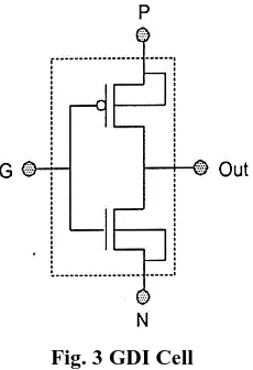
[image:2.595.371.486.345.513.2]In figure [3], Morgenstern proposed basic GDI cells. GDI technique [7] is a new approach to the design of low-power digital combinational circuits, i.e. two transistors implementing complex logic functions that provide cell swing restoration under certain operating conditions. This approach leads to lower power consumption along with low delay in propagation, digital circuit area, and low logic design complexity. An important feature of the GDI cell is that there is no connection between the source of the PMOS in the GDI cell and the source of the NMOS is not connected to the GND. GDI design is more than CMOS design as it has two additional design input pins [6][7].
Fig. 3 GDI Cell
The basic structure of GDI cell is shown in fig 3
1. GDI cell structure consists of one NMOS and one PMOS transistor that looks like a CMOS inverter. In GDI cell, the sources as well as the corresponding transistor substrate terminals are not connected to the supply and can be biased randomly.
2) The GDI cell has three input terminals: 1). G (NMOS and PMOS shorted gate input), 2). P (PMOS source input), and3).N (NMOS source input). The output is taken from D (NMOS and PMOS shorted drain terminal) [9].
Adiabatic CMOS switching
From the above section, it is concluded that large amounts of energy are dissipated through the devices in conventional CMOS circuits in the form of heat and also do not permit the recycling of energy or recovery of energy [6]. These drawbacks made circuit designers go for a non-conventional logic called adiabatic logic or charging logic of recovery or energy recovery logic [14]. Adiabatic is the term taken from thermodynamics and is defined as the process where there is no exchange of energy with the environment and therefore
no dissipation of power. Adiabatic logic uses a time-varying power supply unlike conventional CMOS logic. A linear voltage ramp called the power clock is used for charging and recovering energy from the output and does not switch abruptly from 0 to Vdd and vice versa [15][16].
Consider the same circuit shown in fig 1 for calculating energy consumption for adiabatic logic. Here dual rail time varying power supply is taken instead of constant power supply, which can be input energy into the circuit and recover it back to the power supply.
Fig. 4 (a) Adiabatic Switching [3] Fig. 4 (b) charging Fig. 5 (c) discharging
Figure 3, [6] shows the adiabatic logic model showing an ideal resistance switch in series and two supply voltage clocks complementary. The PMOS transistor is ON and the NMOS transistor is OFF in the first phase when the input is in logic '1' and the power clock rises linearly from zero the capacitor is also charged linearly and the output is in logic '1. When the PMOS transistor is OFF at logic zero and the NMOS transistor is ON. As the NMOS transistor's other end is now connected to the power clock, the energy stored in the capacitor is added to the power clock's energy. Thus, the energy is recovered back to the power supply in the adiabatic logic circuits rather than dissipating to the ground as in conventional CMOS logic circuits. Consider fig 2 for calculating energy consumption, here R is the charging path resistance, which is the combination of the signal line sheet resistance and the transistor's ON resistance in the charging path. Consider the increase in voltage from 0 to 1. To enable vc(t) to follow the V(t) signal.
Current in the circuit is calculated by
i(t) =
---(5)
The energy during charging process is calculated as
E =
. ( ) ---(6)
Since energy is not dissipated in the capacitor for one clock cycle, therefore
Then by replacing with in the equation in equation (6) and putting the value of from equation (5). the result is
E = = ---(7)
Since the whole cycle consists of charging and recovering. The recover process will also lead to the same amount of energy dissipation. Then overall dissipation of Adiabatic logic (AL) is
---(8)
From equation (8) it is observed that the operating speed has impact on the energy dissipation. The slower the circuit charged the lesser the energy is dissipated.
To further reduce the consumption the option of scaling of supply voltage reducing the capacitor load also exists in adiabatic logic which is similar to conventional CMOS .If
equations (4) and (8) are equated ,then T > 4 is the lower
limit of transistion time T which is the value upto which adiabatic circuits are more energy efficient than static CMOS circuits .
[image:3.595.46.480.186.381.2]adiabatic circuit when there is a current flow through the circuit. Each adiabatic circuit consists of digital core made up of
Positive Feedback Adiabatic Logic (PFAL)
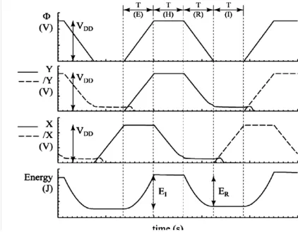
The Positive Feedback Adiabatic Logic (PFAL) achieves the lowest power consumption as opposed to other similar adiabatic logic families [8]. The generalized PFAL circuit diagram is shown in Fig.5. a. The latch is made similar to the 2N-2N2P logic circuit with two PMOS transistors and two NMOS transistors. The functional blocks of NMOS logic are connected in parallel with the PMOS transistors of the latch and form the transmission gates. The fact that the functional blocks are in parallel with the PMOS transistors, the equivalent resistance is smaller during the charging of capacitance.
Antonio Blotti et al [9] proposed and implemented adder using PFAL [9]. The working of PFAL inverter circuit is explained by using the fig.5.
Fig. 5 (a) PFAL Logic Circuit
Fig. 5 (b) Four phase power clock for PFAL
The core of PFAL is an adiabatic amplifier which is a latch made up of two pmos transistors MP1, MP2 and two nmos transistors MN1, MN2 respectively. The main purpose of this amplifier is to have full voltage swing at the outputs Y and .the functional blocks blocks here MX and for inverter is connected parallel to the adiabatic amplifier. PFAL uses four phase power clock Φ(t) as shown in the fig.5. b. Initially it is assumed that X is at high logic level and at low logic level. During evaluate phase the power clock rises from o to Vdd and supplies energy to the circuit due to which MX conducts and output Y follow the power clock. When the power clock reaches VTH, threshold value of MN2 regeneration operation will start. At this time MN2 makes to ground.the charging resistance decreases since MP1 is ON which is parallel to MX [8].
During HOLD phase the power clock is at Vdd, then Y and holds at valid logic levels which can also be used as inputs to other cascaded PFAL logic circuits which have been working in evaluation phase. During recovery phase i.e. power clock Φ(t) gradually decreases from Vdd to 0 the charge stored in the load capacitance connected to output Yis recovered back to the power supply through MP1.The resistance of MP1 increase up to the point, so that MP1 turns OFF and the recovery phase stops.
The residual charge on Y cannot be recovered and it is dissipated in the next cycle. Due to this reason PFAL falls under partial adiabatic logic style. PFAL costumes less energy compared to all styles of adiabatic logic and robust against technological parameter variations [9].
III. IMPLEMENTATION OF COMBINATIONAL
LOGIC CIRCUITS
In this section combinational circuits like full adder, multiplexer, de-multiplexer, encoder and decoder are implemented using conventional CMOS logic, GDI logic and adiabatic logic respectively. All the circuits are simulated using TSPICE TANNER EDA tool at 32nm technology. The observations of power dissipation, area and delay are presented in Table 1 and analyzed the parameters mentioned with graphs in figures
Conventional CMOS combinational logic circuits
Full adder
A full adder is a combinational circuit which performs the arithmetic sum of three bits A, B and carry in from a previous addition and produces the corresponding SUM and CARRY out [10][11]. The Boolean expressions for sum and carry respectively are
Sum = A⊕B⊕Cin ……. (1)
[image:4.595.67.269.285.570.2] [image:4.595.56.267.596.760.2]Fig. 6 Conventional CMOS Full adder [10]
The schematic diagram of full adder circuit for conventional CMOS using TSPICE is shown in Fig.6.
Multiplexer
Multiplexing is the generic term used to describe the operation of sending one or more analogue or digital signals over a common transmission line at different times or speeds [10]. Multiplexer is a special type of combinational circuit which selects only one of ‘n’ given data inputs and route it to the output. The selection of one of the inputs is done by ‘m’ select outputs, with 2m
=n [10]. The schematic diagram of multiplexer circuit for conventional CMOS using TSPICE is shown in Fig.7.
Fig.7.Conventional CMOS Multiplexer
De-multiplexer
[image:5.595.335.517.50.170.2]A demultiplexer is a digital combination with one input and more than one output. It is used when a circuit wants to send a signal to one of the many devices [10]. The schematic diagram of de-multiplexer circuit using TSPICE is shown in Fig.8.
Fig. 8 Conventional CMOS De -Multiplexer
Encoder
[image:5.595.327.523.280.392.2]A simple encoder is one type of combinational circuit. It has maximum of 2n input lines and ‘n’ output lines; hence it encodes the information from 2n inputs into an n-bit code [11]. The schematic diagram of encoder circuit using TSPICE is shown in Fig.9.
Fig. 9 Conventional CMOS Encoder
Decoder
[image:5.595.50.290.457.665.2]A binary decoder is a combinational circuit that converts binary information from the n coded inputs to a maximum of 2n unique outputs. They are used in a wide variety of applications, including data demultiplexing, seven segment displays, and memory address decoding [11]. The schematic diagram of decoder circuit using TSPICE is shown in Fig.10.
Fig. 10 Conventional CMOS Decoder
GDI combinational circuits
[image:5.595.325.534.526.663.2](a)Full Adder (b)Multiplexer
(c)De – Multiplexer (d)Encoder
[image:6.595.108.486.50.488.2](e)Decoder
Fig. 11 Implementation of combinational circuits using GDI Logic
PFAL combinational logic circuits
Full Adder
The schematic diagram for sum of full adder circuit [16] using TSPICE is shown in Fig.12. (a) and the carry circuit shown in Fig.12. (b) output wave form is shown in Fig.12. (c) respectively.
Fig. 12 (a) Adiabatic Full Adder sum circuit
[image:6.595.314.548.516.686.2] [image:6.595.60.280.591.744.2]Fig. 12(c) Adiabatic Full Adder output wave form [20]
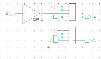
Multiplexer
The schematic diagram of multiplexer circuit [16] using TSPICE is shown in Fig.5.23 and the output wave form is shown in Fig.13
Fig. 13 (a) PFAL Multiplexer
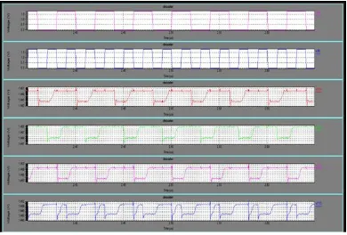
Fig. 13 (b) Output waveform [21]
De multiplexer
The schematic diagram of demultiplexer circuit [16] using TSPICE is shown in Fig.14. (a) and the output wave form is shown in Fig.14. (b)
Fig. 14 (a) PFAL Demultiplexer
Fig. 14 (b) Output waveform [21]
Encoder
The schematic diagram of encoder circuit [18][19] using TSPICE is shown in Fig.15. (a) and the output wave form is shown in Fig.15. (b)
Fig. 15 (a) PFAL Encoder circuit
Fig. 15 (b) Output waveform
Decoder
[image:7.595.314.538.48.232.2] [image:7.595.58.284.51.189.2] [image:7.595.52.296.264.592.2] [image:7.595.319.535.448.652.2] [image:7.595.68.266.653.768.2]
Fig. 16 (a) PFAL Decoder Fig. 16 (b) Output waveform
IV. RESULTS AND DISCUSSION
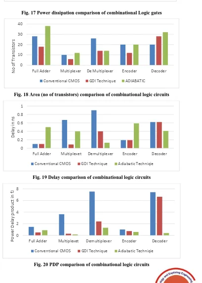
The combinational logic circuits like full adder, multiplexer, demultiplexer, encoder, decoder are implemented and simulated for the three techniques using TSPICE in TANNER tool at32nm technology. In this
[image:8.595.315.510.50.182.2]observation for power dissipation, area, delay and power delay product (PDP) of all the above-mentioned combinational circuits for three logics styles are tabulated in Table.1. The comparison of parameters mentioned, for three logic styles are presented in terms of percentage in Table.2.
Table. 1 Observations for combinational logic circuits
Circuits Conventional GDI Technique Adiabatic
Power (μw) No. of transisto rs Delay (ns) PD P (fJ) Powe r (μw) No.of transist ors Dela y (ns) PD P (fJ) Powe r (μw) No.of transisto rs Del ay (ns)
PD P (fJ)
Full adder 14.72 28 0.1 1.4
7
5.14 18 0.1 0.51 1.77 38 0.5 0.8
85 Multiplex
er
5.45 10 0.67 3.6
5
3.38 6 0.09 0.3 0.41 12 0.4 0.1
6
De-Multiplex er
8.38 26 0.9 7.5
4
6.16 14 0.4 2.4 4.40 14 0.3 1.3
2
Encoder 5.36 20 0.19 1.0
1
3.95 12 0.19 0.75 1.47 20 0.4 0.5
9
Decoder 11.97 20 0.62 7.4
2
10.73 28 0.62 6.65 1.04 32 0.4 0.4
[image:8.595.92.264.65.203.2]1
Table. 2 Percentage comparison of parameters between three logic styles for combinational logic circuits
Logic circuits % variations of parameters % variations of parameters % variations of parameters GDI technique Vs
Conventional logic
Adiabatic technique Vs Conventional logic
Adiabatic technique Vs GDI technique
Power Area delay PDP Power Area Delay PD P
Powe r
Area Delay PD P
Full adder 35 52.6 0 65 71 26↑ 40↑ 39 18 52↑ 40↑ 43↑
Multiplexer 11 40 39 91 92 20↑ 40↑ 98 87 50 30↑ 61
Demultiplexer 10 46 0.45 68 47 46 66 82 29 0 25 45
Encoder 26 40 0 26 72 0 52↑ 42 63 40 52↑ 21
decoder 10 36 0 10 91 0 43 66 97 36 68↑ 63
The ↑ in the Table.2 represent the % increase in the parameters of combinational logic circuits and remaining values are % decreased in the parameters of combinational logic circuits. From the Table.2,itis observed that power savings are more for adiabatic logic style and it is about 91% of power is reduced compared to conventional CMOS logic and 97% of power is saved compared to GDI technique for decoder circuit. For Adiabatic logic style the delay is increased compared to other two logic styles but delay is less for the combinational logic circuits which are
[image:8.595.54.544.294.488.2] [image:8.595.62.538.508.642.2]Fig. 17 Power dissipation comparison of combinational Logic gates
Fig. 18 Area (no of transistors) comparison of combinational logic circuits
Fig. 19 Delay comparison of combinational logic circuits
Fig. 20 PDP comparison of combinational logic circuits
0 10 20 30 40
Full Adder Multiplexer De Multiplexer Encoder Decoder
N
o
o
f Tran
sis
to
rs
Conventional CMOS GDI Technique ADIABATIC
0 0.2 0.4 0.6 0.8 1
Full Adder Multiplexet Demultiplexer Encoder Decoder
De
lay
in
n
s
Conventional CMOS GDI Technique Adiabatic Techniqie
0 2 4 6 8
Full Adder Multiplexet Demultiplexer Encoder Decoder
Pow
er De
lay
p
rod
u
ct in
f
J
Conventional CMOS GDI Technique Adiabatic Techniqie 0
5 10 15 20
Full Adder Multiplexet Demultiplexer Encoder Decoder
P
o
we
r
in
μ
wa
tt
s
[image:9.595.112.521.200.771.2]V. CONCLUSION
The paper presented the implementation of different combinational logic circuits mentioned using different techniques like conventional CMOS switching, GDI technique and Adiabatic logic style. The main objective of the paper is to give the idea how the logic can be implemented by using different approaches depending on the applications. In this it is observed that compared to conventional CMOS logic style the GDI technique implementation consumes less area and less delay but it suffers from non-full voltage swing. But the applications where the area and delay are of important criteria the GDI technique can be selected .it is also noticed that power saving are more for Adiabatic logic style compared to other logic styles mentioned as well as PDP.For the applications where the energy consumption is primary concern adiabatic logic style can be option since this logic style consumes very less power than the logic styles.
Future work can be reducing the area for adiabatic logic styles and to obtain full voltage swing for GDI technique.
REFERENCES
1 Sung-Mo Kung and Yusuf Leblebici, CMOS Digital Integrated Circuits, Tata MaGraw Hill Edition, 2003.
2 Abdullatif Bellaouar and Mohamed I. Elmasry, Low-Power Digital VLSI Design Circuits and System, Kluwer Academic Publishers, 1995, ISBN 0-7923-9587-5.
3 .M.C. Stock, “Technology Leverage for Ultra-Low Power Information Systems”, IEEE Symposium on low power electronics, Tech. Dig., pp. 52-55, October 1994.
4 Gupta, Bunkmates. (2012). Transistor gating: A Technique for Leakage Power Reduction in CMOS circuits. International Journal of Emerging Technology and Advanced Engineering, (2),321-326.
5 S. Kang and Y. Lebleici, CMOS Digital Integrated Circuits-Analysis and Design, Reading chapter McGraw-Hill, 2003.
6 P.Teichmann, "Adiabatic Logic," Springer Series in Advanced Microelectronics, vol. 34, pp. 1-19, 2012.
7 Morgenshtein, A. Fish, I. A. Wanger, “Gate-Diffusion Input (GDI): A power efficient method for digital combinational circuits,” IEEE Trans. on Very Large-Scale Integration (VLSI), vol. 10, No. 5, pp. 566-581, 2002.
8 A.Vetuli, S.Di Pascoil and L.M.Reyneri, "Positive feedback in adiabatic logic," Electron.lett, vol. 32, pp. 1867-1869, 1996
9 Alioto.M and Palumbo, "Power estimation in adiabatic circuits:A simple and accurate model.," IEEE Transactions On Very Large Scale Integration Systems, vol. 9, no. 5, pp. 608-615, 200
10 A. Chandrakasan,S. Sheng and R.Brodersen, (1992)” Low-power CMOS digital design”, IEEE Journal of Solid-StateCircuits, Vol.27, No4, pp.473-484.
11 N. Zhuang and H.Wu , (1992)” A New Design of the CMOS Full Adder”, IEEE journal of Solid-state Circuits, Vol.27, No.5, pp 840-844.
12 Yingtao Jiang, Abdulkarim Al-Sheraidah,Yuke Wang, Edwin Sha, and Jin-Gyun Chung, “A Novel Multiplexer –Based Low –Power Full Adder” IEEE Transaction on circuits and systems-II: Express Brief , Vol.51,No.7,p-345, July-2004.
13 N. Naresh, M.Srinivasulu,” Design and Implementation Various Logic Circuits Using GDI Technique,” VOL.3, Issue 8, August 2015. 14 Pranshu Sharma, Anjali Sharma,”Analysis of power reduction in 2 to 4
line Decoder design using Gate Diffusion Input technique,”Vol.3, Dec 2016.
15 B.Jyothi, K.Vamshi Krishna, M.Basha, A High Speed Low Power Full Adder Using GDI Multiplexer, September (2016).
16 M. Mittal and Anil Khatak, "Design and Analysis of Energy Recovery Logic for Low Power Circuit Design," International Journal of Engineering Research and Applications (IJERA), pp. 20 - 24, 2014 17 A. Blotti and R. Saletti, "Ultralow-Power Adiabatic Circuit
Semi-Custom Design," Ieee Transactions On Very Large Scale Integration
18 Blotti, S.Di Pascoli and R.Saletti, "A comparision of some circuit schemes for semireversible adiabatic logic," Int.J.Electron, vol. 89, pp. 147-158, 2002.
19 Arpan chaudhuri, Mamia saha, and Moumita bhowmik, Implementation of circuit indifferent Adiabatic Logic,” Proceedings of the IEEE, 2015.
20 K. ROY and Y. YE,” Ultra Low Energy Computing using Adiabatic Switching Principle”, ECE Technical Reports, Purdue University, Indiana, as accessed on April, 2013.
Authors
1.T. SUGUNA is a research scholar in E.C.E department, Dr M.G.R Educational and Research Institute. Her area of research is in design of low power VLSI circuits.
![Fig. 4 (a) Adiabatic Switching [3] Fig. 4 (b) charging Fig. 5 (c) discharging](https://thumb-us.123doks.com/thumbv2/123dok_us/8201948.261118/3.595.46.480.186.381/fig-adiabatic-switching-fig-b-charging-fig-discharging.webp)
![Fig. 12 (b) Adiabatic full adder carry circuit [20]](https://thumb-us.123doks.com/thumbv2/123dok_us/8201948.261118/6.595.108.486.50.488/fig-b-adiabatic-adder-carry-circuit.webp)