UNIVERSITI TEKNIKAL MALAYSIA MELAKA
OPTIMIZATION OF MICROSTRIP DIAMOND ANTENNA FOR
DUAL BAND APPLICATION
This report submitted in accordance with requirement of the Universiti Teknikal Malaysia Melaka (UTeM) for the Bachelor Degree of Engineering Technology
Department of Electronic and Computer Engineering Technology
By
NAZMI SYAZWAN BIN NORDIN B071310814
920629-14-5971
BORANG PENGESAHAN STATUS LAPORAN PROJEK SARJANA MUDA
TAJUK: Optimization of Microstrip Diamond Antenna for Dual Band Application
SESI PENGAJIAN: 2016/2017 Semester 1
Saya NAZMI SYAZWAN BIN NORDIN mengaku membenarkan Laposan PSM ini disimpan
di Perpustakaan Universiti Teknikal Malaysia Melaka (UTeM) dengan syarat-syarat kegunaan seperti berikut:
1. Laporan PSM adalah hak milik Universiti Teknikal Malaysia Melaka dan penulis. 2. Perpustakaan Universiti Teknikal Malaysia Melaka dibenarkan membuat Salinan
untuk tujuan pengajian sahaja dengan izin penulis.
3. Perpustakaan dibenarkan membuat salinan laporan PSM ini sebagai bahan pertukaran antara institusi pengajian tinggi
4. **Sila tandakan ( )
SULIT
TERHAD
TIDAK TERHAD
Disahkan oleh:
___________________ ___________________
Alamat Tetap: Cop Rasmi:
___________________________
___________________________
___________________________
Tarikh: ________________ Tarikh: ________________
** Jika Laporan PSM ini SULIT atau TERHAD, sila lampirkan surat daripada pihak berkuasa/organisasi berkenaan dengan menyatakan sekali sebab dan tempoh laporan PSM ini perlu dikelaskan sebagai SULIT atau TERHAD.
UNIVERSITI TEKNIKAL MALAYSIA MELAKA
(Mengandungi maklumat yang berdarjah keselamatan
atau kepentingan Malaysia sebagaimana yang
termaktub dalam AKTA RAHSIA RASMI 1972)
(Mengandungi maklumat TERHAD yang telah
FAKULTI TEKNOLOGI KEJURUTERAAN Tel : +606 234 6623 | Faks : +606 23406526
Rujukan Kami (Our Ref) : Rujukan Tuan (Your Ref) :
1 JUN 2016
Pustakawan
Perpustakaan UTeM
Universiti Teknikal Malaysia Melaka Hang Tuah Jaya,
76100 Durian Tunggal, Melaka.
Tuan/Puan,
PENGKELASAN LAPORAN PSM SEBAGAI SULIT/TERHAD LAPORAN PROJEK SARJANA MUDA TEKNOLOGI KEJURUTERAAN ELEKTRONIK (TELEKOMUNIKASI)(BETT): NAZMI SYAZWAN BIN NORDIN
Sukacita dimaklumkan bahawa Laporan PSM yang tersebut di atas bertajuk
“Optimization of Microstrip Diamond Antenna for Dual Band Application”
mohon dikelaskan sebagai *SULIT / TERHAD untuk tempoh LIMA (5) tahun dari tarikh surat ini.
2. Hal ini adalah kerana IANYA MERUPAKAN PROJEK YANG DITAJA OLEH SYARIKAT LUAR DAN HASIL KAJIANNYA ADALAH SULIT.
Sekian dimaklumkan. Terima kasih.
Yang benar,
_________________________ Tandatangan dan Cop Penyelia
* Potong yang tidak berkenaan
NOTA: BORANG INI HANYA DIISI JIKA DIKLASIFIKASIKAN SEBAGAI
SULIT DAN TERHAD. JIKA LAPORAN DIKELASKAN SEBAGAI TIDAK
TERHAD, MAKA BORANG INI TIDAK PERLU DISERTAKAN DALAM
iv
DECLARATION
I hereby, declared this report entitled “Optimization of Microstrip Diamond Antenna for Dual Band Application” is the results of my own research except as
cited in references.
Signature : ………
Author’s Name : NAZMI SYAZWAN BIN NORDIN
v
APPROVAL
This report is submitted to the Faculty of Engineering Technology of UTeM as a partial fulfilment of the requirements for the degree of Bachelor’s Degree in Electronic Engineering Technology (Telecommunication) with Honours. The member of the supervisory is as follow:
……… MADAM RAHAINI BT MOHD SAID
(Project Supervisor)
………. MD. ASHADI B. MD. JOHARI
vi
ABSTRAK
vii
ABSTRACT
viii
DEDICATION
To my beloved parents
Nordin bin Saad and Norita binti Arshad
To supervisor and co-supervisor
ix
ACKNOWLEDGEMENT
x
TABLE OF CONTENTS
ABSTRAK ... vi
ABSTRACT ... vii
DEDICATION ... viii
ACKNOWLEDGEMENT ... ix
LIST OF TABLE ... xii
LIST OF FIGURES ... xiii
LIST OF ABBREVIATION, SYMBOLS AND NOMENCLATURE ... xv
CHAPTER 1 ... 1
1.1 BACKGROUND ... 1
1.2 PROBLEM STATEMENT ... 2
1.3 OBJECTIVES ... 3
1.4 SCOPE ... 3
CHAPTER 2 ... 4
2.1 ANTENNA PARAMETERS... 4
2.1.1 Radiation Pattern ... 4
2.1.2 Bandwidth ... 4
2.1.3 Polarization ... 5
2.1.4 Return Loss ... 5
2.1.5 Voltage Standing Wave Ratio (VSWR) ... 6
2.2 MICROSTRIP ANTENNA ... 6
2.2.1 STRUCTURE OF MICROSTRIP ANTENNA ... 7
2.2.2 FEEDING TECHNIQUE ... 8
2.3 MICROSTRIP DIAMOND ANTENNA ... 10
2.4 ADVANCED DESIGN SYSTEM (ADS) ... 12
2.5 DESIGN OF EXPERIMENT (DOE) ... 15
CHAPTER 3 ... 17
3.1 IDENTIFYING THE PROBLEM ... 17
3.2 PROJECT PLANNING ... 17
3.3 VARIABLE INDENTIFICATION ... 19
xi
3.3.2 DISTANCE ... 19
3.3.3 FREQUENCY ... 20
3.3.4 POLARIZATION ANGLE ... 20
3.4 METHOD SELECTION (ADVANCED DESIGN SYSTEM) ... 21
3.4.1 DESIGN USING ADS ... 22
3.5 METHOD SELECTION (HARDWARE PROCESS) ... 24
3.5.1 ETCHING ... 24
3.5.2 SOLDERING PROCESS ... 30
3.6 METHOD SELECTION (TESTING PROCESS) ... 31
3.6.1 EXPERIMENT ... 31
3.7 METHOD SELECTION (DESIGN EXPERT 2K FACTORIAL DESIGN) .... 33
3.7.1 CLARIFY AND STATE OBJECTIVE ... 35
3.7.2 CHOOSE RESPONSES ... 35
3.7.3 CHOOSE FACTORS AND LEVELS ... 35
3.7.4 CHOOSE EXPERIMENTAL DESIGN ... 36
3.7.5 PERFORM THE EXPERIMENT ... 36
3.7.6 ANAYLYZE THE DATA... 38
3.8 ANALYSIS ... 38
CHAPTER 4 ... 39
4.1 EXPERIMENT RESULT ... 39
4.2 ANALYSIS RESULT ... 41
4.3 OPTIMIZATION RESULT... 51
4.4 DISCUSSION ... 52
CHAPTER 5 ... 55
5.1 CONCLUSION ... 55
5.2 RECOMMENDATION ... 56
REFERENCES ... 58
xii
LIST OF TABLE
Table 2.1: Comparison of different feeding methods ... 9
Table 2.2: Parametric study of the ground plane's length against bandwidth and return loss. ... 11
Table 2.3: Variable for the 23 experiment ... 16
Table 2.4: 23 factorial experiment ... 16
Table 3.1: Properties of experiment ... 35
Table 3.2: Matrix Design of Experiment ... 37
Table 4.1: Tabulation data of output power of the microstrip diamond antenna ... 40
Table 4.2: ANOVA of output power ... 42
Table 4.3:Optimization Criteria Setting ... 51
Table 4.4:Optimization solutions (the first 5 from 100 solutions displayed) ... 52
xiii
LIST OF FIGURES
Figure 2.1: Structure of microstrip patch antenna 7
Figure 2.2: Common shapes of microstrip antenna. 7
Figure 2.3: Change of length ground plane 11
Figure 2.4: Change of ground plane's length versus bandwidth 12
Figure 2.5: The mesh in momentum simulation 14
Figure 2.6: The example for component of layout 14
Figure 3.1: Progression of the planning project 18
Figure 3.2: Flow chart of designation microstrip diamond antenna by using Advanced
Design System 21
Figure 3.3: Block diagram of ADS Momentum simulation 22
Figure 3.4: Schematic and layout for 2.5 cm microstrip diamond antenna. 23 Figure 3.5: Schematic and layout for 5 cm microstrip diamond antenna. 23 Figure 3.6: The microstrip diamond antenna was printed on transparent paper. 24 Figure 3.7: the transparent paper was pasted on PCB board. 25
Figure 3.8: PCB board in UV process. 25
Figure 3.9: the shaped from transparent paper was transferred to PCB board. 25
Figure 3.10: PCB developer process 26
Figure 3.11: The shaped appeared on PCB boar after PCB developer process. 27
Figure 3.12: Etching process. 28
Figure 3.13: The shaped of antenna after etching process. 28
Figure 3.14: PCB board in etching cleaning process 29
Figure 3.15: PCB board after etching cleaning process 29
Figure 3.16: soldering process. 30
Figure 3.17: the microstrip diamond antenna was attached with SMA connector. 30
Figure 3.18: The operation to obtain output power. 31
Figure 3.19: Data collect at 800MHz and 1900MHz. 32
Figure 3.20: Data collect at distance 15 cm and 30 cm. 32 Figure 3.21: Data collect at polarization angle 90 ˚ and 180 ˚ 33 Figure 3.22: Flow chart of experiment by using 24 Factorial Design 34
Figure 4.1: Normal plot for Output power 43
Figure 4.2:Normal Plot of Residual for Output Power 44
xiv
Figure 4.4: Pareto Chart for effects 46
Figure 4.5:One Factor Effect Plot for Output Power (Dimension) 47 Figure 4.6: One Factor Effect Plot for Output Power (Polarization Angle) 47 Figure 4.7: Interaction Factor Effect Plot for Output Power (Polarization Angle with
Dimension) 48
Figure 4.8: Interaction Factor Effect Plot for Output Power (Polarization Angle with
Distance) 49
Figure 4.9:Interaction Factor Effect Plot for Output Power (Distance with Frequency) 50 Figure 4.10:Interaction Factor Effect Plot for Output Power (Distance with Frequency
xv
LIST OF ABBREVIATION, SYMBOLS AND
NOMENCLATURE
ANOVA - Analysis of Variance ADS - Advanced Design System
EM - Electromagnetic
AUT - Antenna Under Test
DoE - Design of Experiment
EMC - Electromagnetic Compatibility SPC - Spatial Polarization Characteristic
MoM - Method of Moment
VSWR - Voltage Standing Wave Proportion PCB - Printed Circuit Board
1
CHAPTER 1
INTRODUCTION
1.1 BACKGROUND
Antenna is an electrical devices assigned to transmit or catch the electromagnetic (EM) waves by converting the electric signal into wave signal and vice versa. In transmission, a radio transmitter supplies an electric current swaying at radio frequency to the antenna’s terminals, and the antenna emanates the vitality from the present as electromagnetic waves (radio waves. In gathering, an antenna captures a portion of the force of an electromagnetic wave so as the deliver a little voltage at its terminal that is connected to a beneficiary to enhanced. There are many types of antenna and the most famous among other is microstrip antenna, microstrip antenna is an essential element which offers an optimal solution(Mahesh, Gulbarga, 2014). Microstrip antennas is a sort of antennas used to handle ultra-high frequency signals. It is frequently utilized as a satellite radio or wireless beneficiary or is mounted on an airplane or shuttle. This sort of antennas has the point of interest that is cost little to make yet the burden that is has restricted data transfer capacity.
2
Advanced Design System (ADS) one of the famous software design and simulate the microstrip antenna. ADS is an electronic design automation software system produced by Keysight EEsof EDA, a division of Keysight Technologies. It gives a powerful design environment to designers of RF electronic products such as mobile phones, pagers, wireless networks, satellite communications, radar systems, and high-speed data links.
1.2 PROBLEM STATEMENT
Nowadays, antenna technology is growing align with advancement in communication technology where the size of each component become small. Microstrip antenna is most famous among the other antenna because of its physical structure is small size, suitable with the minimal effort and minimized setting for wireless system technology. Microstrip antenna has been utilized in variety functions that also give contribution in communication technology. But in specific uses such as in dual band application.
3
1.3 OBJECTIVES
In this research, the main objectives of this project are:
i. To study and develop microstrip diamond antenna for Dual-Band applications. ii. To identify a significant effect of microstrip diamond antenna parameter for
Dual-Band applications.
iii. To optimize the best combine of microstrip diamond antenna properties for optimizing the performance
1.4 SCOPE
4
CHAPTER 2
LITERATURE REVIEW
2.1 ANTENNA PARAMETERS
2.1.1 Radiation Pattern
Antenna radiation pattern are generally polar awesome circle or equatorial pattern, 2D or 3D patterns. In antenna theoretical one examines the far-field measurement parameters i.e., directivity, gain, phase, polarization and standardized radiation pattern. The latter is the most regularly measured parameter. Exact estimation of radiation pattern includes consideration of various components, for example, the physical and electrical size of the antenna, its operational frequency band, and the environment in which it is to work. Antenna pattern measurement alludes to the determination of the radiation pattern of an Antenna Under Test (AUT). It is the measurement of the relative greatness and phase of an electromagnetic sign got from the AUT. The antenna is a complementary device so the pattern data could be gotten by utilizing it as either the transmitter or receiver. although complex antenna pattern measurement have been a typical necessity in the microwave antenna enclosure for a long time, it has just as of late turn out to be more normal to different ranges, for example, Electromagnetic Compatibility (EMC) and wireless telecommunications (Ullah, Flint, & Seager, 2AD).
2.1.2 Bandwidth
5
been calculated is the data transmission. Its worth relies on upon antenna parameters (thickness and permittivity of each layer). Therefore, the paper shows that as a result of optimization which has been shown we can make a planar antenna with extensive variety of work. The analysis procedure of multilayer microstrip antenna is complex and time consuming (Przesmycki, Bugaj, Nowosielski, & Wnuk, 2011).
2.1.3 Polarization
The value of polarization data has as of now been built up in most remote sensing, target detection, polarization enhancement, polarization filtering, and target recognition applications. Furthermore, the fancied polarization of antenna radiation (i.e. the principle polarization), still can transmit the orthogonal polarization (cross polarization) sign of expectation, and the radiation intensity of cross polarization increments with the deviation of azimuth angle increments. That is to say, the antenna polarization changing in various positions and arranged headings is known as Spatial Polarization Characteristic (SPC) of antenna. (Jianling, Huanyao, Depei, Wenzhao, & Bo, 2015).
2.1.4 Return Loss
6 2.1.5 Voltage Standing Wave Ratio (VSWR)
Voltage Standing Wave Ration VSWR is characterized as the ration of the maximum to minimum voltage of the antenna The reflection coefficient ρ characterize as a proportion between incident wave amplitude Vi and reflected voltage wave amplitude Vr, and by utilizing the meaning of a voltage reflection coefficient at the input terminals of the antenna Γ, as appeared below where Z0 is the characteristic impedance of the antenna. On the off chance that the Equation is solved for the reflection coefficient, it is found that, where the reflection coefficient ρ is the absolute vale of the magnitude of Γ (Elrashidi & Elleithy, Hassan Bajwa, 2012).
𝑟 = 𝑧𝑖𝑛𝑝𝑢𝑡−𝑧𝑜
𝑧𝑖𝑛𝑝𝑢𝑡+𝑧𝑜 𝜌 = |𝑟| =
𝑉𝑆𝑊𝑅−1
𝑉𝑆𝑊𝑅+1 𝑉𝑆𝑊𝑅 =
|𝑟|+1 |𝑟|−1
2.2 MICROSTRIP ANTENNA
7
2.2.1 STRUCTURE OF MICROSTRIP ANTENNA
[image:22.595.181.458.226.387.2]A Microstrip patch antenna comprises of a metal trace on one side of a dielectric substrate which has a ground plane on the other side and design of microstrip patch antenna appeared in figure 2.1. The patch usually is made from conducting metal for example copper or gold and it can be form any possible shape as shown in the figure 2.2. (Parmar, Saxena, & Nayak, 2014).
Figure 2.1: Structure of microstrip patch antenna
Figure 2.2: Common shapes of microstrip antenna.
[image:22.595.182.459.429.611.2]8
patch antennas, high dielectric consistent substrate, for example, ceramic oxide materials are utilized as host substrate. However, their utilization results in some natural issues like trouble in impedance matching, poor effectiveness and narrow bandwidth, excitation of surface waves that could bring down the radiation proficiency and weaken the radiation pattern. To expand the limited bandwidth and radiation proficiency of patch antennas, stacked or slotted patch antennas can be utilized. Bandwidths of 10%-20% have been accomplished with test probe fed stacked patches, and 18%-23% bandwidths have been accomplished for aperture coupled stacked patches (Singhal & Jaimini, 2013).
2.2.2 FEEDING TECHNIQUE
9
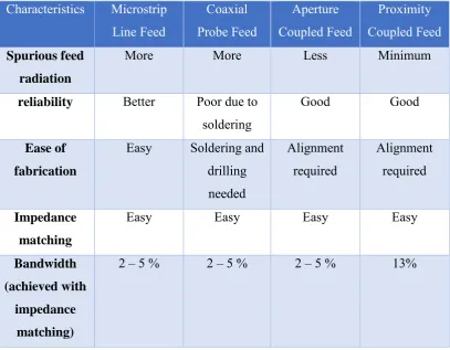
Table 2.1: Comparison of different feeding methods
Characteristics Microstrip
Line Feed Coaxial Probe Feed Aperture Coupled Feed Proximity Coupled Feed Spurious feed radiation
More More Less Minimum
reliability Better Poor due to
soldering
Good Good
Ease of fabrication
Easy Soldering and drilling needed Alignment required Alignment required Impedance matching
Easy Easy Easy Easy
Bandwidth (achieved with
impedance matching)
2 – 5 % 2 – 5 % 2 – 5 % 13%
Advantages of Microstrip Antennas
The major advantages of microstrip antennas are:
Light weight
Low volume
Low-profile planar configuration which can be easily made conformal to host surface
Capable of dual and triple frequency operations Disadvantages of Microstrip Antenna:
Microstrip patch antennas suffer from a number of disadvantages as compared to conventional antennas (Bernard et al., 2013).
Narrow bandwidth
Low efficiency