This thesis is presented for the degree of Master of Science in the Australian National University.
The work described in this thesis is the candidate's own work, except where otherwise stated, or where sections have been included to further the logical development of the discussion at hand.
The work was done during the tenure of an Australian National University scholarship, and was supervised by Professor A.N. Hambly.
The work in this thesis has formed the basis of the following two papers, delivered at the Fourth Australian Spectroscopy conference at Canberra. These papers
were-"The distribution of Atoms in Flames and its signific ance in Atomic Absorption".
C.S. Rann and A.N. Hambly.
"Estimation of Selenium by Atomic Absorption methods". A.N. Hambly and C.S. Rann.
A further paper which has been submitted for public ation is entitled
Assistance is gratefully acknowledged from Dr.DoSo Robertson and Mr.E0 Penikis for many helpful discussions and criticisms concerning the instrumental aspects of this work.
Professor A oN0 Hambly has contributed helpful advice and encouragement throughout all aspects of the project; his ready counsel has been much appreciated 0
SUMMARY
A study has been made of the types of signals occurring in atomic absorption analysis, and the optimum instrumentation needed for handling each case. The source of the limiting noise in this type of measurement has also been investigated
The distribution of atoms in the flame of the standard 10 cm burner has been investigated, and the results have been applied to the improvement of instrumental sensitivity.
The atomic absorption method has been applied to the assay of selenium . The theoretical and practical problems have been studied, and methods have been developed for the analysis for selenium
Acknowledgments. Summary.
CHAPTER I - INTRODUCTION
1.1 Selection of research topics. 1
1.2 General description of apparatus. 3
CHAPTER II - RADIATION DETECTOR
2.1 Introduction. 6
2.2 Photocathode. 6
2.3 Comparison of photomultiplier and photocell. 9 I
2.4 Description of photomultiplier and housing. 11 2.5 Testing the photomultiplier.
2.5*1 Dark current. 13
2.5.2 Gain. 13
2.5.5 Optimum voltage for operation of the
photomultiplier. 14
2.5.4 Voltage between photocathode and first dynode. 15 2.6 Investigation of limiting noise.
2.6.1 Introduction. 15
2.6.2 Noise within the light beam. 16 2.6.3 Dark current and photomultiplier instability. 18
2.6.4 Schottky noise. 19
2.6.5 Conclusion. 21
CHAPTER III - INVESTIGATION OE AMPLIFIERS
3.1 Introduction. 23
3.2 Classification of signals. 25
3.3 Theoretical basis of the techniques used.
3.3.1 Observation time, bandwidth, and time-constant. 27 3.3.2 Relationship of bandwidth and noise. 27
3.4.2 The effect of higher harmonics. 3*5 Square law detector.
3.6 Description of amplifiers. 3.7 Experimental investigations.
3.7.1 Testing with microscope slides.
3.7.2 Testing with weak signals and a flame. 3.7*3 Conclusions.
3.8 Frequency spectrum of noise. 3.9 Flame emission interference.
3.10 Variation of sensitivity with higher harmonics of the modulation frequency.
3.11 Conclusion.
CHAPTER TV - DISTRIBUTION OF ATOMS IN THE FLAME 4.1 Introduction.
4.2 Experimental.
4.3 Effect of the anion. 4.4 Effect of the fuel. 4.5 Effect of the cation. 4.6 Discussion.
4.6.1 "Small area density"technique.
4.6.2 The formation of atoms in the flame. 4.6.3 The shape of the spectral source. 4.6.4 Conclusion.
4.7 Plasma flame.
4.7.1 Introduction.
4.7.2 Spectral properties of the plasma. 4.7-3 Experiments.
4.7.4 Conclusions.
CHAPTER V - ANALYSIS FOR SELENIUM 3.1 Introduction.
5.2.2 Population of the excited states. 70
5.5 Spectral source. 71
5.4 Line intensities from the spectral source. 75
5.5 Elimination of self reversal. 76
5.6 Atomic absorption experiments on selenium.
5.6.1 Equipment. 81
5.6.2 Flame absorption. 81
5.6.5 Sensitivity of the selenium lines. 82
5.6.4 Choice of gas. 85
5.6.5 Variation with anion. 86
5.6.6 Distribution of selenium in the flame. 87 5.6.7 Analysis of selenium in foods. 88
5.6.8 Selenium in minerals. 91
References. 94
CHAPTER I INTRODUCTION 1.1 Selection of research topics
The absorption of atomic spectral lines by atomic
vapour has been known since the time of Bunsen, Kirchhoff, and Fraunhofer. However, the unique advantages of
I
utilising this phenomenon for chemical analysis have only recently been stressed. Walsh in 1955» ( 1 )
first suggested the technique as an alternative to spark and flame emission methods. He pointed out the considerable enhancement in sensitivity that is possible by using absorption instead of emission methods.
In an atomic vapour, the population of the various energy levels is given by the Boltzmann distribution
-n 0
(
1.
1)
where is the energy of an excited state j, and n-j is the number of atoms in this state; n 0 is the pumber of atoms in the ground state; Pj and P0 are the statistical weights for the excited state and the ground state respect ively.
atoms. The absorption method utilises the ground state atoms, hence,a greater sensitivity is to he expected from
i
this method.
The technique of atomic absorption analysis, started by Walsh's group in Melbourne, received initial support mhinly from Australian chemists . Australian and New Zealand workers, such as J.E. Allan, D.J. David, J.B.Willis
I
and others, have been very prominent in the application of the technique to chemical analysis . With this background oj* local development, it was considered that atomic absorp tion analysis should be an appropriate field for research projects in Australian Universities. The particular
aspects of atomic absorption chosen for investigation in this thesis, stem from some of the underdeveloped aspects of the technique, that inevitably occur in a rapidly expanding field of research.
Rees and Walsh of the C.S.I.R.O,, encouraged the rapid development of the technique for use in chemical analysis. With this aim in mind., a simple,but effective apparatus was designed by Box and Wqlsh, ( 2 ) . This equipment was inexpensive, and had the desired effect of putting the new method in many laboratories for evaluation and development. Therefore, rapid development has pro ceeded in the application of atomic absorption in chemical analysis, so that, at present, the literature on this
subject contains contributions on most of the elements likely to be easily analysed by this technique.
This concentration of effort on the application to chemical analysis has left the instrumental side of the method underdeveloped. Before significant advances in
be required of such aspects as the chemistry of the flame, the generation of suitable spectral lines, and the optimum methods for detecting and evaluating the spectroscopic information presented. The first part of this thesis has endeavoured to contribute to this aspect of the development.
The second part of the thesis is concerned with the application of the technique to a group 6B non-metal. The elements which have been studied to date are entirely metallic cations; it is thought that the analysis of an anion constituent represents a new field of application for atomic absorption. Selenium was selected because of a growing awareness of the importance of trace quantities of this element in foodstuffs, and because the present methods of analysis for selenium are neither elegant nor rapid.
1.2 General description of apparatus
Figure (1.1) shows the arrangement of the units used in this work. Light from a spectral source is mechanically chopped, passes through the flame ( into which the solution for analysis is sprayed ) 9and entei's a monochromator. The monochromator is adjusted to refract the resonance line of the element concerned^ onto the photocell. The output of the photocell is amplifled and presented on a meter or chart recorder.
Figure 1.1
f l a m e
m o n o c h ro m a to r
b u r n e r
s p r a y c h a m b e r c h o p p e r 300 c/s
s a m p l e
The power supply for the spectral lamps consisted of an unstabilised 1000V DC source, incorporating a variable resistance in series with the spectral lamp. As this variable resistance constituted the major load of the power supply, the current was considerably stabilised
against changes in lamp resistance, which may Jiave occurred. The spectral lamps used were hollow cathode lamps,
either manufactured by Ransley Glass Instruments, Melbourne, or made in the workshop of the chemistry department.
The chopping disc was driven by a non-synchronous motor at about 2000 revs/min. The disc consisted of eight
segments, which formed the chopping blades.
The burner was the standard 10 cm burner supplied by Stewart R. Skinner Pty. Ltd., Melbourne. Supplies of fuel and compressed air to the burner, were monitored for
pressure and flow rate. Above the burner, a small exhaust hood removed the products of combustion.
The lenses used were made from"Ultrasil" silica, and were designed to match the 1 : 6.7 numerical aperture of the Zeiss reflecting monochromator,(Type SPM3 ,) .
This monochromator has interchangeable prisms made of sodium chloride, silica and glass.
The photocell was an EMI 6256S photomultiplier, which is described elsewhere in this thesis. An Isotopes Dev elopment LimitedC Type 532/D),variable voltage, stabilised, power supply was used to provide the working voltage for the photomultiplier.
Several amplifiers could be used following the photo multiplier, the main unit being a Hewlett PackardC302A)Wave Analyser. A Yarian G-10 recorder could be connected to any
Plate 4.3^shows a general view of the equipment. The rack holds (in order from the bottom), the stabilised photomultiplier supply, the hollow cathode lamp supply, the Hewlett Packard wave analyser, and at the top, a power distribution panel and a scale expansion unit.
The exhaust hood,optical rail, and monochromator are seen on the bench. The photomultiplier housing extends out horizontally from the monochromator. A portable vacuum unit,for the fabrication of spectral sources, is seen near the fume cupboard. This unit contains a mercury diffusion pump, and a mechanical backing pump. Provision is made for the entry of the filler gas,and for liquid air cooling. A variable voltage (up to 2 KV), DC,power supply is also built into the unit,to enable the testing of hollow cathode lamps before sealing,
CHAPTER II
RADIATION DETECTOR
2 • 1 Introduction
The radiation detector is a critical element in the apparatus, and therefore considerable effort was expended in studying the types of detectors available ,and in testing and adjusting the detector that was eventually selected .
In view of the work proposed, the detector had to meet two main requirements.
(a) It must be sensitive to UV radiation down to at least 1900 A.
(b) It must be capable of measuring very weak intensities. A survey of available detectors showed the photomult iplier to be the most sensitive. A photocell could have the same photocathode as the photomültiplier, yet it would be inferior for use with small signals, because of the Johnson noise in the grid resistor of the following amplifier. The photomultiplier escapes this source of noise, amplifying the original .photocathode current by secondary emission,until the signal is so large that any Johnson noise in the load resistor, or other noise from the first amplifier, becomes insignificant. The photo multiplier offers almost noise-free amplification of the photocathode current, as the following analysis will show. 2.2 Photocathode
Under normal conditions the photocathode could be
. oh r
\f'-called upon to produce photo-currents between 10”^ to 10~12 a ( 10^-5 to 107 electrons/sec). The measurement of the lower part of this range will now be investigated.
If it be assumed,that electrons in a conductor carrying an electric current arrive in a random manner,the fluct uation in the rate of arrival is given ( 3 ) by
-(AN2) = N (2.1)
where N is the average number of electrons arriving per unit time, and AN is the difference between the actual number arriving and the mean number N. The root-mean- square of these deviations, ie. V(a n2) can be taken as the standard deviation of the distribution. The emission of electrons from a photocathode is governed by this dis tribution, and is given by the Schottky equation ( 4 ) ,
(In )2 = 2elAf (2.2)
where e = charge of the electron, Af = band width in c/s, and In is the"noise current" (or AI) of the average
current I, where
I = Ne (2.3)
The photocathode,however, may also emit electrons
In order to bring out the important parameters involved, the equation will be derived for an S/N ratio combining the effects of the background noise,and Schottky noise.
If (j) is the number of signal quanta arriving per unit time, and (Q) is the quantum efficiency of the photocathode
*
-x.C the electrons collected at the first dynode per quantum) at the wavelength of the signal, and similarly, (j1) and (Q *) refer to the general thermal radiation , assumed to be causing most of the background current, then
I = ejQ , (2.4)
and the background current
I' = e d ' Q 1 (2.5)
the S/N ratio I
V(In )2+(I')2 (2.6)
Combining equations 2.2, 2.4, 2.5 and 2.6, ejQ
S/N = (2.7)
y
2e2AfJQ + (ej *Q ')2An examination of equation 2.7 leads to the following points concerning the attainment of a high S/N ratio.
(a) The number of signal quanta (j) should be high. (b) The quantum efficiency at the signal wavelength
(Q) should be high.
(c) The number of extraneous quanta (o') should be low. (d) The quantum efficiency (Q') should be low at the
wavelength of the thermal radiation. (e) The bandwidth (Af) should be small.
low, it is usual to amplify it further before measurement,
and this amplification can introduce further noise, thus
causing a lower S/N ratio at the measuring indicator.
2.3 Comparison of photomultiplier and photocell
If a photocell is connected to the grid of a v a cuum
tube amplifier, the load resistor of the cell (which is
the grid resistor of the amplifier) has a Johnson noise
(Ir ) due to the thermal motion of the electrons, ( 5 >6 ).
given by
(Ir )2 4kTAfR
(
2.
8)
k = 1.38 x 10“23 joules/OK.
T = temp. (°K).
Af = bandwidth (c/s).
R = resistance (ohms).
The low values of photocathode current (I) met in
practice necessitate the use of a high resistance. A calcul a t i o n >using some typical values for the various
p a r a m e t e r s ,shows that this can be very detrimental to
the S/N ratio. If a one megohm load resistor is used to monitor a 10” A photocathode current, at 2 7 ° C , the
following S/N ratio could be expected, using a bandwidth
of 10^ c/s. For the photocathode without any dark
current-S/N = --- —
V2elAf
(2.9)
V(In )2+ (Ir )2
V
2elAf+ 4kTAf E 10-12"V 3.2 x 10⁻²⁸+1,7 x 10~22
= 7.8 x 10⁻²
The Johnson noise is approximately 10 times higher than the s4,gpal. To obtain a S/N ratio of 1.0, a photocathode current of the order of 10" H A would be required, or an increase of the load resistor to 10® ohms. Furthermore, the grid current in the first stage of the amplifier will introduce noise. This current would be as high as 10"® A for an ordinary tube, and as low as lO"1^ A for a special electrometer tube,such as the Mullard ME1402. In the above example, an electrometer tube would be used to elim
inate this extra source of noise.
The photomultiplier provides almost noiseless amplific ation of the photocathode current. The photocathode
current is magnified by secondary emission approximately 10® times, and the resulting current overrides any Johnson noise in the load resistor. A fluctuation in the second ary emission at the dynodes does introduce further noise, but, as will be demonstrated, this is comparatively minor compared to that of a conventional amplifier.
The final anode current Ia is given by
-Ia = I G (2.11)
If a photomultiplier has m dynodes, each with a second ary emission coefficient of d, then the gain is given
by-G = dm (2.12)
and gains of 10& and 10® are quite common.
The statistical variation in the secondary-emission coefficient will be a source of noise, and will be most important for the first dynode,and correspondingly less important for each successive dynode. Of all the noise in a photomultiplier, 80 percent is due to the fluctuat ions in the photocathode emission. The remaining 20 per cent is due to the dynode noise . F o r a value of d about 4, 15 percent of the noise would come from the first dyn
ode, 4 percent from the second and 1 percent from the third.
The above considerations suggested a photomultiplier having the following requirements
-(a) Sensitive to UV light, ie. (Q) is large, equation (2.7).
(b) Not sensitive to the red or infra red end of the spectrum, ie, (Q!) is low, to decrease the emission of thermal electrons.
(c) ,A window, preferably of fused silica, to transmit UV light, ie. high (j) in equation (2.7).
2.4 Description of photomultiplier and housing
The final selection was the EMI 6256 S, which is a 15-stage ,Venetian blind, type of photomultiplier. The window was of " Spectrosil", a fused-silica, made by Thermal
o
thermal electrons per sq. cm» per second at 20°C. The oxidised cathode, type S, is claimed to give only 20
electrons per sq.cm.per second under the same conditions. The peak overall quantum efficiency of the S type cathode
o
is about 10 percent and occurs at approximately 4200 A.
o
The sensitivity is useful to 6500 A at the red end, and is limited by the window material at the ultraviolet end. The secondary emitting surface is Sb-Cs and with 13 stages, the limiting gain could be as high as 109. Specifications claim a cathode sensitivity of 30 /UA/L, an overall sensit ivity of 2000 A/L, and a maximum dark current of 0.0025/xA.
The mounting of the tube in the apparatus needed detailed consideration,
(a) The dark current can be considerably reduced by cooling the photocathode in order to reduce thermal electrons. Provision was made for cooling the entire photomultiplier, if it should prove necessary.
(b) Magnetic fields can deflect the electrons in their path from the photocathode, to the first dynode. This could
lead /to less efficient collection of electrons, which would be equivalent to lowering the quantum efficiency of the photocathode. To reduce magnetic fields, a mu-metal screen was mounted between the tube and the outer brass case.
(c) Fluctuations in dark current have been reported (7, 8, 9, 10) due to the proximity of the photocathode (which is at 1500V) to earthed metal objects, such as the shield. Glass wool packing, half-inch thick, was used between the mu-metal shield and the glass of the tube at the cathode end.
the scintillations could get hack to the cathode, there fore all surfaces inside the photomultiplier housing were painted black.
(e) Careful tests were performed to ensure that the photomultiplier housing was light tight when fitted to the exit slits of the monochromator.
2.5 Testing the photomultiplier 2.5.1 Dark current
The tube was mounted in the manner described, the photocathode being at the room temperature,22°C. At 1700V the dark current was 10“8 A, as measured by a
Keithley(200B)micro-micro-ammeter. The readings were
taken after 5 hrs. aging in the dark with voltage applied to the tube.
Two tubes were tested, and gave similar results. The variation of dark current with applied voltage is shown as the bottom curve in fig. 2.1. The manufacturers test
figure for this tube was 5 x 10“9 A at 1750V. 2 0 5o2 Gain
Figure 2.1
Variation of relative gain and dark current with applied voltage
—
2.5*3 Optimum voltage for operation of the photo multiplier
[image:21.574.36.555.61.724.2]2.5*4- Voltage between photocathode and first dynode For optimum S/N ratio, the largest number of photo electrons leaving the cathode should reach the first dynode. This is related to Q in equation 2.7> and must be at a
maximum. For this reason, and also to increase the sec ondary emission coefficient (d) of the first dynode, it is often advised that the voltage should be greater be tween the cathode and the first dynode,than the voltage used between the other dynodes. This was investigated experimentally, and within the accuracy of S/N measure ment was not found to be significant. The .Voltage divider chain,therefore,consists entirely of 100 K resistors.
2.6 Investigation of limiting noise 2.6.1 Introduction
All instruments are eventually limited in their sensitivity by noise of some sort. The following invest igation was carried out to ascertain the source of noise
y * v" '
which limited the detection of very weak signals with
this equipment. In some other instruments used for atomic absorption measurements, especially those using more noisy photocells, the results and conclusions could be different.
A weak signal is defined here as having a S/N ratio of 1.0 (the average amplitude of the signal pulse equals the amplitude of the noise - see fig. 5*2). All subsequent measurements described here were done at this S/N ratio, which was estimated from oscilloscope tracings.
The first investigation concerns the noise inherent in the actual light beam,at this intensity. Next, the sources of noise within the photomultiplier are examined, leading to the identification of the limiting noise found in
2.6,2 Noise within the light beam
The fluctuation in the intensity of a beam of light arises because it is quantised. At the higher frequencies, the energy hV of a photon increases, and the possibility of detecting single photons,.or the fluctuation in the arrival of many photons,increases. The fluctuation in the arrival of quanta is not given by the Bose-Einstein stat istics, or any other similar treatment,which deals with the mean square fluctuation of the distribution of elect rons throughout the various energy levels at equilibrium. In this type of treatment, conservation of energy is ass umed, not a conservation of the number of photons. The statistics in the present case must deal with a stream of photons which have no means of interacting with each other, and thus cannot alter their quantum state. It must be
assumed that the photons arrive at random, but at an aver age rate proportional to the beam intensity. The number incident per unit time ,will be given by a Poisson distrib ution, in which the mean square fluctuation in the number of arrivals will equal the mean number of arrivals, ie.
(ä ü2 ) = d (2.13)
I
which is similar to equation (2.1).
If the quanta arriving are not monochromatic, the relative numbers of photons of different energy values will be
subject to fluctuations governed by Bose-Einstein statistics. In the present discussion, it is assumed that monochromatic light only is used.
The following calculations investigate the fluctuations of the incident light, when the photomultiplier is working at the limit of detection; defined here as the incident
light which causes a S/N value of 1.0 at the photomult iplier anode»
The number of incident quanta (j),of energy h V ,arriving in unit time, gives a measure of the power or intensity of the incident light.
W = JhV (2.14)
The fluctuation in the arrival of the quanta is given by equation (2.13), thus
S/N = j
VC
Ad2)
(2.15)
• As the photo tube manufacturer gives the photocathode sensitivity in terms of m A/lumen, calculations are
facil-o
itated if light of 4000 A is used, because at this wave length the following equalities apply
:-<
mA / watt = j u k / lumen
1 watt = 668 lumens.
The EMI 6256 S photomultiplier tested had an anode current of 3°3 A A,when S/N ratio of 1.0 was measured at the anode. Assuming a gain (G) of 108 , the photocathode current (I) is obtained from the anode current (Ia ) by
-la
I »-Jr- (2.16)
3.3 x 10⁻⁶
108
= 3.3 x 10“1^ A (2 x 10⁵ electrons/sec.)
Using the manufacturers value for the average photo cathode sensitivity (40 M A/lumen), the flux of the incid ent light falling onto the photocathode is
/
3.3 x 10“ 14 4 X 10⁻⁵
Thus the intensity,or power of the incident light,at the threshold of detection is 1.23 x 10“ 12 watt, or 1.23 x 10“ 5 erg/sec. - if the light has a wavelength of 4000 A.
For light of this wavelength,hV = 4.95 x 10"12 erg. Thus from equation (2.15)
S/N 1.23 x 10“!? 4.95 x 10“12
1.58 x 10³
In this case there are 2.5 x 10^ quanta falling on the photo-cathode per second.
The S/N ratio of the incident light is approximately 103 times better than the S/N ratio of the signal result ing at the photomultiplier anode. Obviously then, the limit of detection is not being set by fluctuations of the incident light.
2.6.3 Dark current and photomultiplier instability At the voltage used in this experiment, the average anode current was 3 »3 x 10⁻⁸ A,and the dark current was 10-8 a . Therefore the ratio of signal current/dark current
3.3 x 10⁻⁶ 10-8
330
which is far removed from the actual S/N value of 1.0. Therefore it is concluded that the dark current is not seriously affecting the S/N ratio at this light level.
If the photomultiplier were the cause of a less obvious source of noise, for example, that caused by optical feed back or by ionisation of the residual gas in the photomult iplier, it would be expected that the S/N ratio would
v e r y high voltages were used, at which point heavy noise
resulted from ionisation of the residual gas in the tube.
It is thought unlikely that the limiting noise is from a
source of this nature.
2.6.4 Schottky noise
The "shot noise", or "noise in signal", mentioned in section 2.2, can be very serious for small currents.
This noise arises from the random nature of the emission
of electrons from the p h o t o c a t h o d e ,when light falls upon
it, and has no connection with the dark current,or "thermal
electron" emission from the cathode. The Schottky equation
governs the noise current (In ) at the cathode.
In2 = 2eIAf (2.17)
As (I) cannot be measured directly, this equation can be
stated in terms of the anode current (Ia ).
T 2 _ 2eIaAf
-L n
---G
(2.18)
where Ia = 1 G (from equation (2.16))
S/N
(2.19)
As G and Af are not exactly known, the first method used
for investigating this effect eliminates their influence.
If the S/N ratio is taken at two different light levels,
then the ratio of these values will be given by
-( S / N ) !
(S/N)" ■(la)"
Hence the ratio of S/N ratios should be given by the square root of the respective signal currents.
Table 2.1 gives the results of four such measurements. As the signal is measured by the voltage across the anode
load resistor, equation (2.20) can be restated in terms of voltage.
(S/N)» (S/N)"
U a ) ’
(i«)n
(Ea )' (E*)"
(
2.
2 1)
Table 2.1
Comparison of relative S/N ratios with the observed S/N ratio
S i g n a l E a / (Ea)’ Observed
Volts
V (Ea)" S/N
20 4.47 4.0
10 3 o 16 3.3
5 2.24 2.1
1 0 o
1—
1 1.0
It is apparent,from the results in Table 2.1,that the S/N ratio is dependent on the strength of the incident light. As the measurement of S/N ratio, especially for low values of this ratio, was not particularly precise, the results in the second and third columns in Table 2.1 are considered to agree within the accuracy of measurement.
[image:27.574.40.574.80.694.2]between 4 - 4 . 5 . As there are 1$ dynodes, and if d is taken as 4.12, the gain given by equation (2.12) is
(4.12)15 = 10Ö, which is quite a reasonable value to assume for this photomultiplier. Using a G Af value of 10^3 in equation (2.19),the expected S/N ratios are cal culated from the measured anode currents. The results are presented in Table 2.2. Again it is considered that the results agree within the accuracy of the S/N measure ment .
Table 2.2
Comparison of the calculated S/N ratio with the observed S/N ratio
^-a Observed S/N Calculated S/N
66.6 4.0 4.56
33.3 3.3 3.25
16.6 2.1 2.28
3.3 1.0 1.04
2.6.5 Conelusion
It is concluded from the above investigation that the limit in the measurement of weak signals is set by the "noise in signal", or the random nature of electron emission at the photocathode. As this is a fundamental limitation, no further attempts were made to improve the photomultiplier.
Three further conclusions were obtained frpm this investigation.
(a) Cooling the photomultiplier will not lead to a significant improvement in accuracy.
[image:28.574.67.556.61.714.2]CHAPTER III
INVESTIGATION OF AMPLIFIERS
3.1 Introduction
The amplifier is expected to amplify the signal from the photomultiplier, so that a meterf or other form of indicator can display the result to the operator. The amplifier could, if necessary, have very high gain.
However, such "instrumental sensitivity", if taken beyond a certain point, would not lead to further improvement in the instrument. If the function of the amplifier were only to provide sensitivity, then the design of such a unit would be straightforward.
It is not generally realised that an amplifier provides two other important functions.
(a) The amplifier can "select" information within the signal.
(b) The amplifier can present an average value from a fluctuating signal.
In this work,the word "amplifier" is used rather loosely to include any unit used for processing the signal from the photomultiplier. In some cases,no amplification occurs.
middle of each trace,the same dilute solution (contain ing copper) was sprayed. The traces were obtained successively over the period of a few minutes, all settings of the equipment remaining unchanged, except for the alteration of the amplifier as specified. The designations w/b and n/b refer to wide band (Af-10^c/s), and narrow band (Af=6c/s),amplifiers respectively * The technique of scale expansion is not dealt with in this work, as it represents a method of obtaining greater instrumental sensitivity, but does not improve the S/N ratio,
Figure 3 „1
Improvements in the readability of a weak absorption the amplifier design
The change in the 100% line is recorded when a very dilute solution is sprayed
into the flame. In each case the sol ution has been sprayed during the middle section of the recording.
(a) - wide band amplifier.
(b) - wide band amplifier with integration. (c) - narrow band amplifier and integrat
ion .
(d) - as for (c) with scale expansion.
The criterion used here for a good amplifier is the ability to provide an "accurate" measurement, the sensitiv ity of the amplifier being a secondary consideration. The meaning of "accurate" measurement should be defined as closely as possible. The absorption method virtually
by means of
measures the density of the flame, and the optics are such that a specular density is produced. A good amplifier
will be defined as one that can measure the specular density of the flame at a specific wavelength.
It should be pointed out at this stage that density is not inherently required, transmission values or any other read ings can give accurate assay results, providing the analyst adopts the calibrating techniques used at present in atomic absorption analysis.
3.2 Classification of signals
The types of signal the amplifier is called upon to handle in atomic absorption are classified below.
(a) The normal signal - which has a S/N ratio about 10
.
0.
(b) The weak signal - in which the instrumental noise, and/or extraneous light sources cause a S/N ratio of 1.0 or less.
(c) The drifting signal - where the intensity of the light source is changing with time.
(d) The noisy signal - which differs from the weak signal in that the light source is strong but is fluctuating violently, eg. a spark or arc source. Each type of signal requires a different type of pro cessing by the amplifier to ensure optimum results. In the work described here, four types of amplifier have been investigated, both theoretically and experimentally, for their ability to deal with the varying conditions listed above.
[image:32.574.74.549.85.722.2]Figure $.2 Oscilloscope tracings taken at the photomultiplier anode, showing the range of signals encountered from a modulated spectral source.
Tracing "a" represents strong signal conditions, usually the monochromator slits are wide, and the photomultiplier volt age low.
Tracing "b", r,c", and "d" rep resent the range of S/N ratios encountered by an analyst in day to day use of atomic ab sorption analysis.
[image:33.574.25.554.64.721.2]3-3 Theoretical basis of the techniques used
3.3ol Observation time, bandwidth and time constant
The parameters of bandwidth (Af), time-constant (RC), and observation time (T) ,are interdependent. The equations (3.1) and (3.2) indicate the general depend ence of each parameter on the other, ( 11 ), although slightly different relationships are often used, (3 ).
1
Af (3.1)
2RC (3.2)
Thus from equation (3.1), we see that the time constant, or "response time" of an amplifier is related to the recip rocal of the bandwidth (or pass-band). Equation (3.2) suggests that the minimum time of observation should be at least twice the time-constant of the system.
If it is decided to use an amplifier with a very narrow pass-band Af, eg„Af = 1 c/s, then the output meter appears to be damped, and the analyst must spray the sample longer in order for the needle to reach the final position. A similar result is produced when using a wide band amplifier with a long time constant built into the output circuit. The higher the value of R C , the greater the damping^and the longer the observation time.
Large time constants are often used in "averaging" a fluctuating signal. The greater the time constant, the less the fluctuation on the output meter; time must be traded for accuracy.
3o3o2 Relationship of bandwidth and noise
This can best be studied by considering the quad
hence - (En?) = (Enq2) -f (En2^)-h---- (3*3) If noise from each small frequency interval Af (eg. Af = 1 c/s) is combined, then
-___ i=
(En?) = i=
(Eni2)Afi (3.4)
where Eni = the noise voltage contribution per unit frequency for the*i*”th frequency interval Afi-
If it is further assumed that each frequency interval contains the same quadratic content of noise (Eni?), ie.
"white" noise, then
-(En2 ) = (Eni2 ) A? (3.5)
where / A f ± = A f .
The root-mean-square noise output (En) from an amplifier is thus proportional to the square root of the bandwidth
(AF). ie. (En)
(Eni) V aF (3.6)
If a signal comes from a source with a pass-band of 10 kc (ie„ a response time of 0.1 m sec.), and is passed through a filter or ah amplifier with a pass-band of 625 c/s (response time 1.6 m sec. ), the noise will decrease by a factor of four, ie.
. 4
V
625 ' 25 " 3.3.3 Improvement thresholdfrom the flame. Light from the spectral source is modulated electrically, or with a chopper disc, so that the signal from the photomultiplier contains an alternating component at the modulation frequency. An amplifier,responding to this frequency,can then he used to measure the desired signal, the other signals having relatively little effect.
From the discussion in 3*3*2 it would appear that use could he made of this technique in reading very weak sig nals hy simply narrowing the pass-hand of the amplifier.
If, for example, we take a weak signal that is only one fifth as strong as the accompanying noise, ie. S/N = 0.2 when measured in a system with a 10 kc bandwidth, then the S/N ratio should he increased to 20.0 hy decreasing the bandwidth to 1 c/s. Unfortunately this approach has limit ations. As the S/N ratio becomes smaller, a point is
reached where a decrease in bandwidth does not lead to further improvement. This ’’threshold of improvement" usually occurs when the S/N ratio is about 1.0.
3*4- Synchronous detectors 3*4-. 1 General theory
The best known method of dealing with signals having S/N < 1.0, is the phase sensitive detector. Some form of rectifier is designed to activate the amplifier when the desired signal is present. If a modulating frequency of 300 c/s were being used, then a rectifier switching pulse of the same frequency and phase as the modulated signal, would discriminate heavily in favour of the desired signal.
The working of this type of amplifier can best be shown by taking the Fourier series for the rectifier switching pulse (a square wave) and the signal (in this example a sine wave). These signals are multiplied (as the apparatus
is so designed that removal of either signal will result
in zero output), and an expression is formulated which gives
the average output voltage obtained over the observation
time (T).
The switching pulse of the rectifier will be a square
wave given by the Fourier expansion
cos Wt + cos 3Wt i. cos 5Wt .
3
5
In the case of a signal of amplitude Aq and frequency
(angular velocity) Wq, where Wq / nW
A i
Yq = — C O S Wqt
A r and Aq are the p - p amplitudes of the signal.
The result of the multiplication of these two signals is
ApAi
Y rYi ( C O S Wit ) (cos Wt + o o s ^ l t +cos ^Wt + _ --- )
The average value of this function over a period T is given by
-ArAf
t=T
t =0
(cos Wit) (cos Wt + C0S3 ?Wt + C 0 S ^ Wt - )
_ AjAj s in )■£ sin(W-W])t . sin(W]-3W)t , 4T [ 2 (W+ W q ) + 2(W-Wq) + 2(Wq-3W) +
A rAq
As T — 00, 0
T
0
Since all frequencies where Wq / nW produce zero output
as T — »-00, then v e r y little noise will register in the
output, the .effect of noise will be smaller as the
time-'constant, and hence the time of observation, becomes greater.
If the signal is of the same frequency and phase as the
switching signal of the rectifier, ie. Yp = Aq cos W t , then the following analysis applies.
AjxA.1
YrYl = 4 (cos W t )(cos Wt + ° ° s 3 W t c o s 5 W t ----} The average value over a period T is
t=T
ApAi
t=0
, Cos Wt cos 5Wt , cos Wt cos 5Wt cos w c -f. -7 -f- f
-4-A r-4-Ap t sin 2Wt sin (2W)t sin(4W)t
4
- — 27;---4
- — 27;— +2 + 4W 4W 8W
As T — oo,this function
-A-iAj
8A signal, of the same frequency and phase as the detector switching signal, will therefore give a finite output.
Amplifiers using this principle are called synchronous detectors, phase Sensitive detectors, coherent detectors, auto-correlators, homodyne amplifiers etc., and are char acterised by their ability to measure signals when the S/N ratio is <1.0.
3®402 The effect of higher harmonics
During this study,it became necessary to investigate the contribution to the output made by the higher harmonics of the modulated signal, in the case of the synchronous
detector.
cos nWt each other.
In the following analysis, all the cross products of
different harmonic frequencies, and the cross products
for identical frequencies have been evaluated separately.
If the rectifier switching waveform he
. n= oo A r v—
(where n is odd, and designates a particular harmonic)
and the signal waveform
he-A S V ^ 00
Y s ■ “
L
1(where m ps odd, and designates a particular harmonic).
As the waves are of the same frequency and phase, the
product
cos mWt
Yy»Y A
jA-s
n=00 m= oc
r xs
'n=r m=l
cos nWt n
_
cos mWt
dt.
can be resolved into the cross products where n / m and
the cross products where n = m.
Case (1), any two harmonics where n ^ m, will give
ArAs 4nm
(cos nWt)(cos mWt)
The average value of this function over a period T is
t=T
(cos nWt)(cos mWt)
i ^
t = 0 L
ArAs
4nmT
d t .
ApAg 4nmT
sin (n+m)Wt sin (n-m)Wt
ApAs
As T -- ^ ° ° » 4 n m T -- v ^ ence the whole product approaches
zero for long observation times.
Case (2), any two harmonics where n = m
For observation time T, the average value t=T
cos2 (nW)t
j
d t .= 0
ApAs
4 n 2 T
As T
ooproduct-2 +
ArAs
8 n 2
sin (2 n W )t 4nW
a finite result.
The output of a synchro
nous amplifier will be the sum of the cross products of
the identical harmonics in the two wave forms involved,
and will be mostly dependent on the fundamental and the lower harmonics. The average output over a long period
is given by
Y Yir is
n= oo
'n=l
A pA<
8n 2
(where n is odd and designates a particular harmonic)
ApAs
ApAg 8ArAs
8 81
+
n= oo
n=l
1
o + + "^5 +'
32
52
72
Si
8
(
3
.
7
)
A study of equations (3.7) and (3*8) shows that
about 80 percent of the output comes from the fundamental frequency, i e . n = 1; the third harmonic (n = 5) only contributes l/9fand the fifth harmonic (n = 5) only 1/2 5, of the fundamental contribution.
In the apparatus assembled for this work, the rectifier switching waveform was a square wave, but an analysis of the harmonics (measured with the Hewlett Packard wave
analyser) of the modulated signal, showed the distribution in table 3 »5? page 45» As the amplitude of the higher har monics falls off even more rapidly than that of a square wave, then the output was even more dependent on the fund amental frequency.
3.5 Square law detector
It is now apparent that the ability of an amplifier to measure a signal accurately does not depend only on the bandwidth, time constant, and period of observation. The S/N ratio has to be known before the selection of the best type of amplifier can be made. Once the type of detector has been decided, then the techniques of narrowing the band width or increasing the time constant,can be used as approp riate.
One type of detector, not considered so far,
is the square law detector. With this type of det ector the output voltage is proportional to the square of the input voltage, ie.
E0 = aE±2 (3.9)
Ej_ = input voltage. E0 = output voltage.
= proportionality constant.
output, when the S/N ratio is > 1 . 0 at the input. The signal being of greater amplitude than the noise, is
*
enhanced further. As this detector is not linear, the true density of the flame is not measured (indeed grat- ifyingly high values of sensitivity would be obtained by an analyst), so this type of detector will not be consid
ered further.
3.6 Description of amplifiers
Four types of amplifiers were investigated. A brief description of each follows.
A wide band amplifier was representative of present commercial instruments, where the light source is mod ulated at 50 - 100 c/s,and an amplifier with a bandwidth of approximately 10 kc/s is used.The amplifier assembled for this experiment had a bandwidth of 80 c/s - 12 kc/s, at the 5db points. The output of the amplifier could feed a meter or chart recorder if desired, and switching fac ilities allowed variation of the time constant in the out put circuit. The circuit used is shown in fig. 3*5.
A narrow band amplifier was used to investigate the actual improvement attained by narrowing the pass-band,
as discussed in section 5.3.2. The amplifier was a Hewlett- Packard Model 302A wave analyser. The block diagram of
this equipment is shown in fig. 5.6. The unit is virtually a voltmeter that is tuneable over the band 0-50 k c . A
a n d a c o a i p c n e n t o f t h e i n p u t s i g n a l , a r e i n s u c h a r e l a t
i o n s h i p , t h a t t h e d i f f e r e n c e f r e q u e n c y ( l o w e r s i d e b a n d )
i s 100 k c / s . The b a n d o f 0 - 5 0 k c / s i s s c a n n e d m a n u a l l y
b j t u n i n g t h e l o c a l o s c i l l a t o r b e t w e e n 100-1.50 k c / s , a n d
t h e a m p l i t u d e o f t h e t u n e d s i g n a l i s m e a s u r e d by t h e m e t e r .
F i g u r e 5 . 5
C i r c u i t o f w i d e band a m p l i f i e r
0 01 Mf
O u t p u t m a t t r
F i g u r e 3 «6
C i r c u i t o f n a r r o w b a n d a m p l i f i e r
)MAX »*UT VQtTACCl ICARRlCR PAL I | RANGE j I METER C A il
IZEROSCH IfREQUCNCTl LOCAL OSCILLATOR
Figure 3.3
lAAAAAAß
t
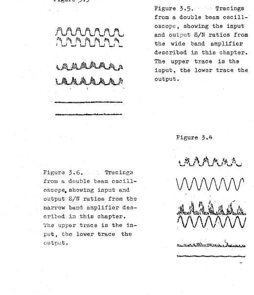
Figure 3*5. Tracings from a double beam oscill oscope , showing the input and output S/N ratios from the wide band amplifier described in this chapter. The upper trace is the
input, the lower trace the output.
Figure 3*6. Tracings from a double beam oscill oscope, showing input and output S/N ratios from the narrow band amplifier des cribed in this chapter. The upper trace is the in put , the lower trace the output.
[image:44.574.43.548.47.725.2] [image:44.574.33.552.118.721.2]Because of the narrow bandwidth of this amplifier, the chopper disc would be required to rotate at constant speed, otherwise the desired signal would drift out of the pass- band of the amplifiero This effect is overcome by an aut omatic frequency control (A.F.C.) facility, built into the wave analyser. Using this control, the analyser "locks" itself onto the signal, so that any variation in the speed of the chopper disc does not affect the output reading. The output was connected to a Varian G— 10 recorder,and a variable time-constant network was coupled to the recorder
input.
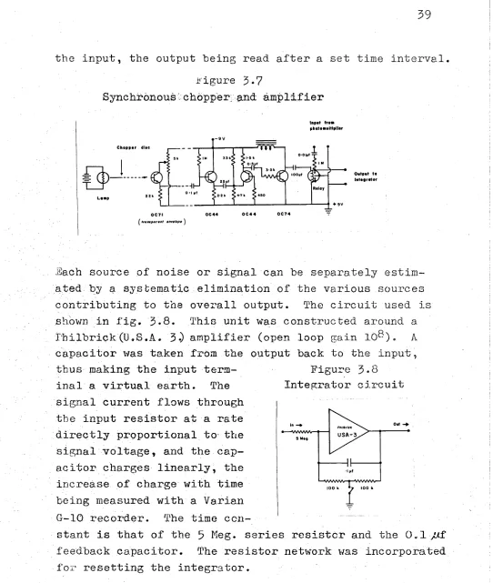
A synchronous amplifier was used to investigate the recording of weak signals, where the S/N ratio was below 1.0. The amplifier, designed and constructed by Dr. D.A. Robertson and staff, used a DC chopper relay driven by a transistorised amplifier, fig. 3»7• The signal used to operate the relay was obtained from a photo-transistor
(an 0C71 with the paint removed) and torch globe mounted at the circumference of the chopper disc. The unit pro duced driving pulses at exactly the frequency of the sig nal, the phase was adjusted by rotating the photo-trans istor unit circumferentially around the chopper disc, and phase comparison with the signal was done by means of a double beam oscilloscope. The signal was fed through this relay,and into the electronic integrator described later.
The unit was tested by illuminating the monochromator slit with light from two sources; one modulated (signal), and the other unmodulated (noise). With a S/N ratio of 0.03, the noise signal could be switched on or off without causing any variation in the reading of the desired signal.
the input, the output being read, after a set time interval.
figure 3*7
Synchronous chopper and amplifier
In p u t fr o m p h o t o m u lt ip lie r
C h o p p e r d ie c
--- HH
OC 4 4 O C 7 I
^ tra n s p a re n t anratopa
Each source of noise or signal can be separately estim
ated by a systematic elimination of the various sources
contributing to the overall output. The circuit used is
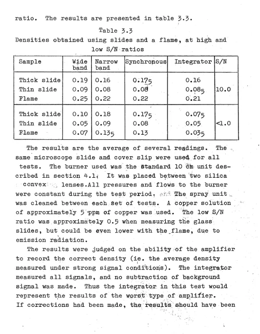
shown in fig. 3*8. This unit was constructed around a
I hilbrick (U oS .A . 3*) amplifier (open loop gain 10®). A
capacitor was taken from the output back to the input,
Figure 3*8
Integrator circuit thus making the input term
inal a virtual earth. The
signal current flows through
the input resistor at a rate
directly proportional to the
signal voltage, and the cap
acitor charges linearly, the
increase of charge with time
being measured v/ith a Varian
G-10 recorder. The time c o n
stant is that of the 3 Meg. series resistor and the 0-1 /tf
feedback capacitor. The resistor network was incorporated
[image:46.574.24.566.49.690.2]3*7 Experimental investigations
3.7«1 Testing with microscope slides
The first requirement for the amplifier is that it he capable of measuring the correct density under ideal signal conditions. (A non-linear amplifier will not meet this requirement). This aspect was checked by using
o
microscope cover slips as standard densities. The 3248 A line of copper was used - at this wavelength the micro scope cover slips had a specular density of 0 .0 7-0 .0 8. All slips checked had the same density within the limits
of error of the apparatus. Microscope slides having a density of 0.16 were also used in checking.
Cover slips were placed in front of the entrance slit to the monochromator, and normal to the optic axis.
Accuracy and linearity were ascertained by successively placing extra cover slips in the optic path, one at a time. A typical set of results, with a good S/N r a t i o n s
shown in table 3 .1.
[image:47.574.57.559.43.718.2]Table 3.1
Density measurements of microscope cover slips, using three experimental amplifiers
No. of Wide band amp. Narrow band amp. Integrator cover
slips D AD D AD D AD
1 Oo0795 0.080 O.O7I9 0 . 0 7 2 0.082s 0.083
2 O.I6I7 0.082 0 01452 0.073 0.1467 0.064 3 0.2418 0.080 0.213i 0 . 0 7 0 0 . 2 2 2 4 0 . 0 6 5
4 O o3 1 2 9 0o071 0 .2 9 0 2 0.073 0.2936 0.073
It should he noticed that the wide hand amplifier gives a higher average reading, and whilst the difference is inside the experimental error of the apparatus (estimated at about 0.01 unit of density),this amplifier may he slightly non linear, as later results in table 3*3 also show the wide hand amplifier gives enhanced values,when high S/N ratios are used. The figures given for the wide hand amplifier could he compared with those obtained by Dr. D.J.David,of the C.S.I.R.Oo, Plant Industry - table 3.2. These read ings, for similar cover slips,were done with a commercial wide band amplifier (Techtron W.M.A. unit),and do not show the same enhancement.
Table 3.2
Density measurements of microscope cover slips, using the "Techtron W.M.A." amplifier ^
No. of cover slips D AD
1 0.076 0.076
2 0.143 0 . 0 6 ?
3 0 . 2 2 2 0 . 0 7 9
4 0 . 2 9 2 0.070
Average 0 . 0 7 3
by D r .DoJ.David, CoSo I . R . O . , Division Industry.
Plant
This suspected discrepancy in the wide band amplifier was not considered to be of sufficient consequence to require a modification of the unit.
3.7 «2 Testing with weak signals and a flame
The next test examined the ability of the four
ratio. The results are presented in table 3 «3» Table 3-3
Densities obtained using slides and a flame, at high and low S/N ratios
Sample Wide
band
Narrow band
Synchronous Integrator S/N
Thick slide 0.19 o 0 1—1 (D
0.17 5 0.16
Thin slide 0.09 0.08 0.08 0 • 08^ 10.0
Flame 0.25 C\ J C M 9 o 0.22 0.21
Thick slide 0.10 0.18 0.175 O.O75
Thin slide 0.05 0.09 0.08 0.05 <1.0
Flame 0.07 0 o 13^ 0.13 O.O35
The results are the average of several readings. The same microscope slide and cover slip were used for all
tests. The burner used was the standard 10 din unit des cribed in section 4.1. It was placed between two silica convex lenses.All pressures and flows to the burner were constant during the test period. The spray unit was cleaned between each Set of tests. A copper solution of approximately 5 sppm of copper was used. The low S/N ratio was approximately 0.5 when measuring the glass slides, but could be even lower with the flame, due to emission radiation.
The results v/ere judged on the ability of the amplifier to record the correct density (ie. the average density measured under strong signal conditions). The integrator measured all signals, and no subtraction of background signal was made. Thus the integrator in this test would represent the results of the worst type of amplifier.
[image:49.574.55.563.73.725.2]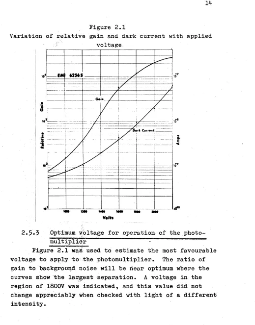


![Table 3*4Variation of density with chop]per harmonics](https://thumb-us.123doks.com/thumbv2/123dok_us/1807677.135901/52.574.56.572.66.693/table-variation-of-density-with-chop-per-harmonics.webp)
