Rochester Institute of Technology
RIT Scholar Works
Theses Thesis/Dissertation Collections
8-1-2009
Methodologies for power analysis attacks on
hardware implementations of AES
Kenneth James Smith
Follow this and additional works at:http://scholarworks.rit.edu/theses
This Thesis is brought to you for free and open access by the Thesis/Dissertation Collections at RIT Scholar Works. It has been accepted for inclusion
Recommended Citation
Methodologies for Power Analysis Attacks on
Hardware Implementations of AES
by
Kenneth James Smith Jr
A Thesis Submitted in Partial Fulfillment of the Requirements for the Degree of Master of Science in Computer Engineering
Supervised by
Assistant Professor Dr. Marcin Lukowiak Department of Computer Engineering
Kate Gleason College of Engineering Rochester Institute of Technology
Rochester, New York August 2009
Approved By:
Dr. Marcin Lukowiak
Assistant Professor, RIT Department of Computer Engineering Primary Adviser
Dr. Dhireesha Kudithipudi
Assistant Professor, RIT Department of Computer Engineering Committee Member
Dr. Mike Kurdziel
Thesis Author Permission Statement
Title: Methodologies for Power Analysis Attacks on Hardware Implementations of AES Author: Kenneth James Smith Jr
Degree: Master of Science Program: EECB
College: Kate Gleason College of Engineering
I understand that I must submit a print copy of my thesis or dissertation to the RIT Archives, per current RIT guidelines for the completion of my degree. I hereby grant to the Rochester Institute of Technology and its agents the non-exclusive license to archive and make accessible my thesis or dissertation in whole or in part in all forms of media in perpetuity. I retain all other ownership rights to the copyright of the thesis or dissertation. I also retain the right to use in future works (such as articles or books) all or part of this thesis or dissertation.
Print Reproduction Permission Granted:
I, Kenneth James Smith Jr, herebygrant permissionto the Rochester Institute of Tech-nology to reproduce my print thesis in whole or in part. Any reproduction will not be for commercial use or profit.
Kenneth James Smith Jr Date
Inclusion in the RIT Digital Media Library Electronic Thesis & Dissertation (ETD) Archive
I, Kenneth James Smith Jr, additionally grant to the Rochester Institute of Technol-ogy Digital Media Library (RIT DML) the non-exclusive license to archive and provide electronic access to my thesis or dissertation in whole or in part in all forms of media in perpetuity. I understand that my work, in addition to its bibliographic record and abstract, will be available to the world-wide community of scholars and researchers through the RIT DML. I retain all other ownership rights to the copyright of the thesis or dissertation. I also retain the right to use in future works (such as articles or books) all or part of this thesis or dissertation. I am aware that the Rochester Institute of Technology does not require reg-istration of copyright for ETDs. I hereby certify that, if appropriate, I have obtained and attached written permission statements from the owners of each third party copyrighted matter to be included in my thesis or dissertation. I certify that the version I submitted is the same as that approved by my committee.
Dedication
This thesis is dedicated to Tim Garwood, Jake Czapeczka, and Andy Fitzgerald for being
there with me on the front lines. Also to all the future scholars including my sisters Katie
Acknowledgments
I would like to thank my advisor, Dr Lukowiak for his patience and guidance. My
com-mittee members Dr Kudithipudi and Dr Kurdziel have offered their valuable time and it
is much appreciated. I would also like to thank fellow students John Frye, Cory Merkel,
Abstract
Side Channel Attacks (SCA) exploit weaknesses in implementations of cryptographic
func-tions resulting from unintended inputs and outputs such as execution timing, power
con-sumption, electromagnetic radiation, thermal and acoustic emanations. Power Analysis
Attacks (PAA) are a type of SCA in which an attacker measures the power consumption
of a cryptographic device during normal execution. An attempt is then made to uncover
a relationship between the instantaneous power consumption and secret key information.
PAAs can be subdivided into Simple Power Analysis (SPA), Differential Power Analysis
(DPA), and Correlation Power Analysis (CPA).
Many attacks have been documented since PAAs were first described in 1998. But
since they often vary significantly, it is difficult to directly compare the vulnerability of
the implementations used in each. Research is necessary to identify and develop standard
methods of evaluating the vulnerability of cryptographic implementations to PAAs.
This thesis defines methodologies for performing PAAs on hardware implementations
of AES. The process is divided into identification, extraction, and evaluation stages. The
extraction stage is outlined for both simulated power consumption waveforms as well as for
waveforms captured from physical implementations. An AES encryption hardware design
is developed for the experiment. The hardware design is synthesized with the Synopsys
130-nm CMOS standard cell library. Simulated instantaneous power consumption
wave-forms are generated with Synopsys PrimeTime PX. Single and multiple-bit DPA attacks are
performed on the waveforms. Improvements are applied in order to automate and improve
The attacks on the simulated power waveforms are successful. The correct key byte is
identified in 15 of the 16 single-bit attacks after 10,000 traces. The single-bit attack which
does not uniquely identify the correct key byte becomes successful after 15,000 or more
traces are applied. The key byte is found in 36 of the 38 multiple-bit attacks. The main
contribution of this work is a methodology and simulation environment which can be used
Contents
Dedication. . . . iii
Acknowledgments . . . . iv
Abstract . . . . v
1 Introduction. . . . 1
1.1 Advanced Encryption Standard . . . 1
1.2 Side Channel Attacks . . . 5
1.3 Power Analysis Attacks . . . 7
1.4 Scope of Work . . . 14
2 Background . . . . 15
2.1 Simple Power Analysis . . . 15
2.2 Differential Power Analysis . . . 16
2.3 Correlation Power Analysis . . . 20
3 Previous Work . . . . 22
3.1 Initial Work . . . 22
3.2 Single-Bit DPA . . . 22
3.3 Multiple-Bit DPA . . . 23
3.4 Correlation Power Analysis . . . 24
3.5 Improved DPA Attack . . . 26
4 Hardware Designs . . . . 29
4.1 Simple Circuit . . . 29
4.2 Custom Iterative . . . 36
5 Simulated Power Extraction . . . . 50
5.1 Design Synthesis . . . 51
5.2 Power Simulation . . . 52
6 Evaluation Algorithms . . . . 59
6.1 Algorithm Design . . . 61
6.2 Maintaining Precision . . . 64
6.3 Performance Improvements . . . 64
7 Results Analysis. . . . 68
8 Conclusions and Future Work . . . . 78
9 Physical Power Extraction . . . . 80
9.1 Overview . . . 80
9.2 Development Platform . . . 82
9.3 Power Measurement Configuration . . . 88
9.4 Oscilloscopes . . . 90
List of Figures
1.1 AES Top Level . . . 1
1.2 AES s-box . . . 2
1.3 AES ShiftRows Operation . . . 3
1.4 AES MixColumns Operation . . . 3
1.5 AES Add Round Key Operation . . . 4
1.6 AES Key Schedule . . . 4
1.7 Mathematical Representation of Cipher Encryption Operation . . . 5
1.8 Indirect Implementation Outputs . . . 6
1.9 Indirect Implementation Inputs . . . 7
1.10 Power Trace Showing DES Software Execution [2] . . . 9
1.11 Power Consumption Resulting from 8-bit Values Transmitted Over Large Data Bus [6] . . . 11
1.12 Power Analysis Factors and Dependencies . . . 12
2.1 General DPA Target Relationship . . . 16
2.2 AES Specific Target Relationship . . . 17
2.3 Differential Power Analysis Evaluation Process . . . 18
2.4 Differential Power Analysis Expected Results . . . 19
3.1 Simulation correlation [9] . . . 26
3.2 Hardware correlation between measurement and predictions [9] . . . 27
4.1 Simple Circuit Top Level General . . . 30
4.2 Simple Circuit Single Data Bit Architecture . . . 31
4.3 Simple Circuit System Control State Diagram . . . 32
4.4 Simple Circuit Top Level Testbench . . . 33
4.5 Useful Altera Synthesis Directives [18] . . . 34
4.6 Simple Circuit System Control Waveform . . . 34
4.7 Simple Circuit Logic Locked Placement and Routing Map . . . 35
4.9 Custom Iterative Top Level . . . 39
4.10 Custom Iterative State Diagram . . . 40
4.11 Custom Iterative Datapath . . . 41
4.12 Custom Iterative Mix Columns Mode Diagram . . . 45
4.13 Custom Iterative Resource Utilization . . . 47
4.14 Custom Iterative Resource Utilization by Entity . . . 47
4.15 AES Core Modules Coordination [10] . . . 48
4.16 AES Core Modules Memory [10] . . . 49
5.1 Top Level Simulation Flow . . . 50
5.2 Hardware Synthesis and Simulation Executable Generation Flow . . . 51
5.3 Hardware Synthesis and Simulation Executable Generation Commands . . 52
5.4 Hardware Synthesisdc shellcommands . . . 53
5.5 Simulation Flow . . . 54
5.6 Simulation Commands . . . 55
5.7 Simulation Executable Commands . . . 56
5.8 PrimeTime PX Simulation Commands . . . 57
6.1 Evaluation Algorithm Accumulate Design . . . 61
6.2 Selection Function Definition . . . 62
6.3 Selection Function Threshold . . . 63
6.4 Translating a Time into an Index . . . 66
7.1 Differential Trace of the Correct Key . . . 69
7.2 Custom Iterative Hardware Simulation Waveform . . . 70
7.3 Single Bit DPA Final Confidence Ratios . . . 71
7.4 Single Bit DPA Confidence Ratio as Traces are Applied . . . 72
7.5 Lowest Resulting Confidence Ratio Extended to 100,000 Traces . . . 73
7.6 Multiple Bit DPA Final Confidence Ratios . . . 74
7.7 Multiple Bit DPA Confidence Ratio as Traces are Applied . . . 75
7.8 Highest Resulting Confidence Ratio Extended to 100,000 Traces . . . 76
7.9 Final Correct Confidence Ratio Comparison . . . 77
9.1 Top Level Physical Flow . . . 81
9.2 Altera Cyclone III Development Board [11] . . . 83
9.5 Development Board FPGA Core Power Bulk and Decoupling Capacitors [12] 87
9.6 Power Measurement Configuration . . . 88
9.7 Cyclone III Architecture [16] . . . 89
9.8 TDS 3012B Configuration . . . 91
9.9 TDS 8000B Configuration . . . 92
9.10 Agilent HP 54810A Configuration . . . 94
List of Tables
4.1 Simple Circuit Control Registers . . . 31
4.2 Mix Columns Byte Ordering . . . 43
4.3 Custom Iterative Mode Decode . . . 45
4.4 Custom Iterative Mix Columns Multiplication . . . 46
6.1 Evaluation Algorithm Memory Requirements (bytes) . . . 66
6.2 Evaluation Algorithm Performance Improvements . . . 67
9.1 Physical Power Extraction Concerns . . . 80
9.2 FPGA Core Bulk and Decoupling Capacitor Values . . . 87
Chapter 1
Introduction
1.1 Advanced Encryption Standard
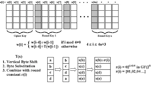
The Advanced Encryption Standard (AES) is a symmetric key block cipher. Data is
en-crypted or deen-crypted in blocks of 16 bytes. Figure 1.1 shows the order in which bytes are
written into the state as plaintext and read from the state as ciphertext [5].
Figure 1.1: AES Top Level
The state is manipulated internally during a variable number of rounds. There are 10,
12, or 14 rounds required for cipher keys of length 128, 192, or 256 bits respectively.
MixColumns, and AddRoundKey. The cipher key is expanded into round keys which are
combined with the state during each round [5]. The following description assumes a 128-bit
cipher key.
The arithmetic required to implement AES functionality is performed in the Galois
FieldGF(28). Therefore, addition and subtraction are identical and performed modulo 2.
Multiplication between two bytes can be performed with a polynomial representation. Each
byte is represented as a polynomial with the bits as coefficients. Multiplication is performed
as is done with conventional polynomials except modulo an irreducible polynomial. The
irreducible polynomial chosen for the standard is shown in below [5].
m(x) =x8 +x4+x3+x+ 1 (1.1)
The SubBytes operation independently transforms each byte of the state. This operation
provides non-linearity and algebraic complexity. SubBytes is comprised of an inversion in
GF(28) and an affine transformation. SubBytes can be implemented as a look-up table
(Figure 1.2) or calculated dynamically [5].
Figure 1.2: AES s-box [5]
shifted [5].
Figure 1.3: AES ShiftRows Operation
The goal of the MixColumns operation is to provide vertical diffusion. Each column
in the state is transformed into a new column. Each byte is considered a coefficient in a
polynomial. This polynomial is then multiplied by a constant polynomial (3x3+x2+x+2)
modulo an irreducible polynomial (x4 + 1). This multiplication can be represented as a
matrix multiplication as shown in Figure 1.4. MixColumns is an invertible operation [5].
Figure 1.4: AES MixColumns Operation
The purpose of the AddRoundKey operation is to combine the cipher and round keys
with the state. This is accomplished with a byte for byte XOR operation. Figure 1.5 shows
this operation [5].
The cipher key is expanded into round keys with the key schedule. One column of the
Figure 1.5: AES Add Round Key Operation
are generated by combining the bytes of the immediately preceding column with the
col-umn four places back. However, the shaded colcol-umns are calculated by first transforming
the previous column with the operation defined asT(x)below.
Figure 1.6: AES Key Schedule
The first step in theT(x)transformation is to vertically shift the column bytes. Then
an s-box byte substitution is performed on each byte in the column. Finally, the first byte
taking successive powers of the byte 0x02 in the GF(28). The expansion continues until
the required number of round keys are generated [5].
These operations are performed as represented in Figure 1.1 in order to encrypt blocks
of plaintext. The decryption process requires the operations to be inverted and performed
in reverse order [5].
1.2 Side Channel Attacks
Traditionally, cryptanalysis has focused on the plaintext, ciphertext, and secret key of
sym-metric key ciphers as the only relevant sources of information considered during an attack.
Analysis is often completed with only a mathematical model of a cryptographic function.
In such a scenario, only data inputs and outputs are considered relevant. It is assumed that
attackers have absolutely no access to secret key information. This model assumes that the
cryptographic processes are ideal black box functions. In reality, implementations of these
processes are not ideal and interact with the surrounding environment. This interaction
may leak some information. If this information is related to the secret key, attackers can
use it to their advantage [7].
Figure 1.7: Mathematical Representation of Cipher Encryption Operation
Side Channel Attacks attempt to relate such an interaction with the environment to
the internal functioning or data contained in a specific implementation of a cryptographic
function. Such a relationships are side channels of information which leak information
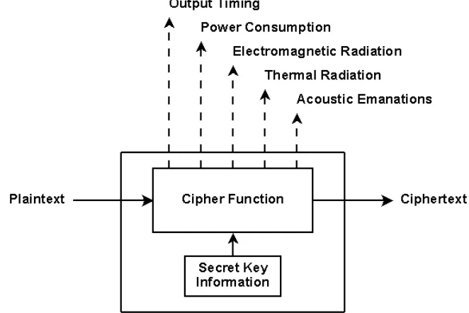
There are several possible sources through which information can leak. Any
measur-able characteristic of an implementation can be exploited as it likely correlates to the
in-ternal functioning of the device. Examples of measurable characteristics are timing, power
consumption, electromagnetic radiation, thermal, and acoustic emanations.
Specific Side Channel Attacks have been developed to exploit these emanations and
their relationship to the internal operations of the implementation. Such Side Channel
Attacks include Timing Attacks, Power Analysis Attacks, and others. With these attacks,
the relationship between secret information and side channel information can be exploited
[image:19.612.141.472.294.515.2][7].
Figure 1.8: Indirect Implementation Outputs
Not only do implementations often react with the surrounding environment through
un-intended outputs, but unun-intended inputs as well. Environmental conditions or inputs that
affect how a device functions can also be manipulated in order to make a device more likely
to reveal unintended information. This is commonly known as fault analysis [7]. Such
attacks often include inducing faults and studying the resulting behavior of the
this difference in behavior can give the attacker additional information up to and
includ-ing secret key information. This type of analysis can include temporarily or permanently
damaging the implementation in order to learn more about internal functionality.
Figure 1.9: Indirect Implementation Inputs
Complete evaluation of the strength and security of a cryptographic function requires
consideration of Side Channel Attacks during the design, implementation, and testing
stages. Research is needed in order to identify and develop standard methods of
evalu-ating the vulnerability of cryptographic implementations to Side Channel Attacks.
1.3 Power Analysis Attacks
Power Analysis Attacks are a type of Side Channel Attack where the power consumption
of an executing implementation is used to reveal secret key information [7]. The power
consumption of an implementation can be measured and recorded as it executes. This is
referred to as the instantaneous power consumption. Power Analysis Attacks exploit a
relationship between the instantaneous power consumption and the changing internal state
Power Analysis Basics
There are three important steps required for any successful Power Analysis Attack. Each
step represents a part of the overall process which allows secret information to be identified
based on the instantaneous power consumption:
• Identify: Find relationship between secret key information and instantaneous power
consumption.
• Extract: Develop method of extracting the state of the relationship information.
• Evaluate: Use this information to determine all or part of the secret key information.
The first step is toidentifya relationship between secret key information and
instanta-neous power consumption. Such a relationship varies depending on many factors.
There-fore, this step must be repeated for each specific instance where an implementation is
at-tacked through Power Analysis. Identification focuses the attack on a specific target which
guides the remaining steps of Power Analysis. It includes identifying the inputs which must
be provided, the outputs which are to be measured, and during which part of the execution
the power consumption will be captured.
Once a specific relationship is identified, a process must be developed in order to
ex-tract the state of the relationship during execution. The identified relationship will be
evaluated many times. Each time, the power consumption must be measured and recorded
at a specific instant during execution. This step includes developing a power measurement
configuration, a specific sequence of operations, and an overall process to automate the
capture and storage of power traces and related information.
The extract step provides many power traces, each with accompanying inputs and/or
outputs and any other additional information. Finally, it is necessary to develop a method
to evaluate the relationship in each of these traces. The raw power consumption traces
and additional information are processed in order to determine the most likely value for the
Extracted Information
Power Analysis Attacks identify, extract, and evaluate a relationship between bits of secret
key information and instantaneous power consumption. There are two ways in which these
are related: algorithm level and data bit level power consumption. These are two ways in
which the instantaneous power consumption pattern can change based on data values being
manipulated.
Figure 1.10: Power Trace Showing DES Software Execution [2]
Figure 1.10 shows the instantaneous power consumption of an instruction processor
ex-ecuting a software implementation of the Data Encryption Standard (DES). The 16 rounds
of the cipher are clearly represented through the repeating pattern of the power consumption
trace [2]. This trace shows how the sequence of operations executed at the algorithm level
are often expressed through the instantaneous power consumption. Usually the execution of
different operations require different amounts of power. These differing amounts of power
are also usually relatively independent of the data values being manipulated. Therefore, by
examining the power trace, it is often possible to infer to some degree what operations are
taking place at which time.
The expression of the operations being executed over time through the power trace can
be helpful to attackers in general. It can be used to set up more powerful attacks by
iden-tifying at which point during an execution to focus on the power consumption. However,
if the sequence of operations executed depends upon the data values being manipulated,
in this way.
Data dependent execution is sometimes a part of the original algorithm specification.
This may also not be part of the original algorithm, but could be added during
implemen-tation. Implementations differ from the original functional specification often in order to
optimize a specific characteristic such as power, throughput, or latency. Although the AES
algorithm is specifically designed to avoid algorithm level weaknesses. It may still be
pos-sible to add such a vulnerability during implementation.
Variations in instantaneous power consumption are also related to the actual data values
being manipulated [7]. As each bit of data is processed, it consumes power as it charges
and discharges hardware interconnects. This power consumption variation is much more
subtle than the large scale variations based on the sequence of operations performed. These
variations are more difficult to detect and may require modifications to the hardware and/or
statistical techniques in order to identify and correlate the variations. Techniques which
utilize power consumption variations based on data values are much more valuable and
powerful for attackers.
Figure 1.11 shows the instantaneous power consumption of an 8-bit HC05
micropro-cessor. The diagram shows the power consumption when an 8-bit value is loaded into a
register from memory. The number of bit transitions are annotated. As more bits transition
from logic zero to logic one, more power is consumed [6].
It is important to note that the degree to which the instantaneous power consumption
varies due to the transmission of data values is almost entirely dependent on the hardware
architecture of the target implementation. The variation in Figure 1.11 is very pronounced
because a large data bus is being charged and discharged. Smaller hardware features result
in more subtle power consumption variations which may not be visually identifiable.
Power Analysis Dependencies
Successful Power Analysis Attacks are a complex coordination of many factors. Figure
Figure 1.11: Power Consumption Resulting from 8-bit Values Transmitted Over Large Data Bus [6]
Analysis results depend upon the specific implementation, the power measurement
config-uration, system control and automation, and the evaluation algorithms used.
Details of the implementation under investigation are very important. The
implementa-tion itself depends on the characteristics of the device it is running on. The cryptographic
algorithm on which the implementation is based describes the functional inputs and
out-puts. Arguably the most important part is the hardware architecture which the
implemen-tation is run on or describes.
The hardware architecture defines the manner in which the data values are manipulated
and transported. Therefore, it also defines the degree to which the manipulation and
trans-portation of specific data values affects the power consumption. Smart cards with
instruc-tion processors are often more vulnerable since the informainstruc-tion is often travelling across
large buses. Such large interconnects require more power to charge than short
intercon-nects. Custom hardware implementations usually have smaller and shorter interconnects
and more parallel processing. This arguably makes them more resistant to power analysis
attacks.
The success of an attack depends to a great degree upon the power measurement
digital sampling oscilloscope is used to sample the voltage across a resistor in series with
the power source. Up to a certain point, faster sampling is always better. More samples in
less time allows for a higher resolution of the power trace. Digital oscilloscopes sampling
in the range of 1 GHz have been used for such attacks [2]. Often trade-offs must be made
between sampling precision, duration, and space required to store power traces.
A lot of thought and effort can be put into the control of the system. This includes
the configuration, coordination, and automation of all of the other components required for
Power Analysis Attacks.
Finally, there are several methods used to evaluate the resulting power traces gathered
from the device under test. The specific method used as well as the manner in which it
is implemented can affect everything from the accuracy of the results to the performance
of the overall attack. These evaluation algorithms are usually software implementations
which process many power traces offline after they have been gathered.
Specific Power Analysis Attacks
There are several specific types of Power Analysis Attacks described in research. The three
main types of power analysis techniques are Simple Power Analysis (SPA), Differential
Power Analysis (DPA), and Correlation Power Analysis (CPA). Related attacks include
us-ing emitted electromagnetic radiation. DPA can be performed with both sus-ingle and multiple
target bits. CPA uses a power model of the unit under test which can be developed using
either Hamming Weight or Hamming Distance to estimate power consumption.
• Simple Power Analysis
• Differential Power Analysis
– Single Bit
– Multiple Bit
– Hamming Weight
– Hamming Distance
The biggest difference between these attacks is the way in which the extracted power
consumption is evaluated. SPA usually involves the visual inspection of power traces for
large scale differences. DPA utilizes statistical techniques in order to identify very subtle
variations in power consumption due to differences in the data values being manipulated.
CPA correlates a power model of the unit under test to the actual instantaneous power
consumption.
1.4 Scope of Work
This research outlines a methodology which can be used to perform Power Analysis
At-tacks on hardware implementations of AES. The main contribution of this work is the
de-velopment of an instantaneous power consumption simulation environment leveraging the
latest Synopsys EDA tools with a 130-nm standard cell library. The environment can be
used to design hardware which is resistant to Power Analysis Attacks. The vulnerability of
different implementations can be directly compared. This evaluation of implementations
allows a design to be strengthened against attacks before being physically implemented.
The result of this is a reduction in vulnerability after less time and with lower costs.
An attempt is also made to attack the physical hardware implementation. This did not
result in a unique identification of the correct key guess. Although this attempt did not
result in a successful attack, it has been documented and is available for future research to
Chapter 2
Background
2.1 Simple Power Analysis
Simple Power Analysis (SPA) is the most basic form of power analysis and the easiest to
defend against or avoid. It involves inspecting power traces for large scale differences based
on the operations performed. Implementations where the execution sequence depends on
the data values being manipulated are more vulnerable than implementations with an
inde-pendent and static execution sequence [7].
Higher operating frequencies and parallel computations usually render hardware
imple-mentations less vulnerable to SPA than software impleimple-mentations. It is sometimes possible
to discern exactly which instruction is being processed in a software implementation by
examining the power trace [1]. SPA often makes it possible to reveal the hamming weight
of data values being manipulated during execution of a software implementation [6].
The design of a cryptographic function can make it much less likely to suffer from
SPA vulnerabilities brought on by the implementation. Ciphers designed with consistent
operations independent of the underlying data are less likely to result in vulnerable
imple-mentations. The design of AES avoids such operations which makes it more resistant to
this type of attack.
When SPA is unsuccessful, it can still be used to set up more advanced power analysis
attacks. SPA can be used to identify which power samples will be used in further analysis,
2.2 Differential Power Analysis
The goal of Differential Power Analysis is to guess secret key information. In order to
accomplish this goal, a relationship must be identified between secret information and
in-stantaneous power consumption. One way to establish this relationship is to identify and
observe a combination of secret and known data and make a prediction about the result.
This prediction or expected value is the target data. The power consumption is correlated
to the target data. Therefore, the correct key guess results in a calculated target value which
correlates to the actual power consumption. Figure 2.1 shows two general ways in which
this relationship can be established. In both scenarios, a combination is performed which
involves known, unknown, and expected data.
Figure 2.1: General DPA Target Relationship
DPA attacks can either be known/chosen plaintext or known ciphertext attacks. A
por-tion of the secret key is guessed. Then the target data is calculated. A main assumppor-tion is
that the target data values are related to instantaneous power consumption. Therefore, the
plaintext and the key are also related to the instantaneous power consumption.
Figure 2.2 shows how this general relationship can be adapted specifically for the AES
cipher. The relationship associated with the input plaintext includes the initial
with the output ciphertext also includes the ShiftRows operation. However, this is a
super-ficial change which only changes the order of the bytes in the state.
Figure 2.2: AES Specific Target Relationship
This relationship is used in the evaluation process. Figure 2.3 describes the evaluation
process for a single key guess. For each plaintext and power trace pair, a selection function
uses the calculated target data to determine which of two groups of traces the current trace
will be associated with. Each group is half of a differential pair. Each trace in the
differen-tial pair is created by summing and accumulating traces associated with it. After all traces
have been accumulated, one trace of the differential pair is subtracted from the other. This
results in one differential trace for each key guess.
Figure 2.4 represents results one would expect from a subset of the entire evaluation
process. The colored dots represent samples in multiple power traces. White dots represent
samples with a slightly higher power consumption. Black dots represent power
consump-tion samples with a lower power consumpconsump-tion. In this representaconsump-tion, a single power trace
is composed of ten samples and one is outlined in a blue line.
Twenty traces have been separated into two groups, this is done once for the correct key
guess and once with an incorrect guess. One group is associated with an expected target bit
equal to one and the other equal to zero. With the correct key guess, the expected target bit
when the power consumption is affected by the target bit. In this model, one sample in each
trace is affected by the power consumption when a target bit is produced by the hardware
and charged on transmit lines.
Figure 2.4: Differential Power Analysis Expected Results
When the correct key guess is used, all of the samples at the target time have a slightly
lower power consumption in one group and a slightly higher power consumption in the
other group. When these traces are averaged, all other variations in the power traces are
averaged to some nominal value. The difference of the differential pairs will reveal a large
spike when the correct key guess is used to calculate the expected target value. Such a
spike does not occur with the incorrect key guess. An incorrect key guess causes the power
traces to be grouped in a way which has no meaning. This is how the correct key guess can
As more power traces are used during an attack, uncorrelated power differences in
the differential trace are further reduced. The result of this is that the differential trace
associated with the correct key guess is easier to uniquely identify from the others.
Differential Power Analysis Attacks are more powerful than SPA [1]. They are also
more difficult to defend against than SPA. DPA uses statistical analysis of power traces in
an attempt to correlate smaller power consumption variations to secret key information.
Error correction techniques can also be applied in order to refine these relationships. This
analysis allows DPA to utilize information not only from high level operations, but also
from the data values being manipulated [1].
2.3 Correlation Power Analysis
Correlation Power Analysis is related to DPA. However, CPA requires more detailed
knowl-edge of the design of the system under attack. A model of the power consumption of a small
target execution sequence of the hardware is built. The resulting power consumption of the
model is compared to the actual power consumption of the device under test. The power
trace of the model should correlate well with the power trace of the device under test when
the two share the same target data bits [9].
In CMOS hardware circuits, the largest power consumption variation occurs when there
is a change in the voltage level of the output or intermediate values of the circuit. Therefore,
models of hardware power consumption focus on the number of bit transitions present [9].
Two models of hardware power consumption are suggested for CPA. These are called
the Hamming Distance and Hamming Weight models [6]. The Hamming Distance or
tran-sition countis a measure of the number of bits that transition during an operation on data.
The Hamming Weight model assumes that the power consumption is most related to the
number of active bits resulting from an operation [9].
Since a hardware power model is necessary to conduct CPA, this model can be used
success of an actual physical attack. The success of a simulated attack when compared to
Chapter 3
Previous Work
3.1 Initial Work
Power Analysis was first described by Kocher in 1998 [1] and 1999 [2] while working at
Cryptography Research, Inc. This initial work describes how and why the power
consump-tion of an implementaconsump-tion can be related to secret informaconsump-tion. It outlines the basics of SPA
and DPA. Both papers describe the steps and theory behind attacking a DES
implementa-tion.
3.2 Single-Bit DPA
A paper by Aigner and Oswald in 2000 [4] presents the fundamentals of Single-Bit DPA
while demonstrating such an attack on a software implementation of DES. The goal was
to determine six bits of a subkeyblockwhich is related to the secret key. The attack only
requires a set of ciphertexts from the encryption process. The key used in the encryption
is unknown. A power trace of the last encryption round is associated with each ciphertext.
A target bit is selected which can be determined by solving backwards from the ciphertext
assuming knowledge of the correct subkeyblock. This process of solving backwards is
called a selection function. The selection function therefore categorizes the ciphertexts
Since the selection function also relies on the subkeyblock, the correct subkeyblock
will allow the selection function to correctly differentiate two groups of ciphertexts and
power traces. The wrong subkeyblock will cause the selection function to separate the
power samples in a way that makes the two groups statistically indistinguishable. Aigner
and Oswald use the moments of the distributions of the power traces in order to
charac-terize them statistically. Specifically, the statistical mean is used to estimate the expected
value of each distribution of power samples. Therefore, for each subkeyblock guess, the
difference between the means of the power samples in the two groups created by the
selec-tion funcselec-tion is calculated. If done correctly, there will be a spike in the difference between
the means of the distributions associated with the correct subkeyblock. This exposes the
correctsubkeyblockwhich is secret information related to the key [4].
3.3 Multiple-Bit DPA
A paper by Messerges in 2002 extends the idea of basic single-bit DPA [6]. The technique
is applied to a software implementation of DES. A selection function is used as with
single-bit DPA in order to separate the power traces and ciphertexts into groups. With multiple-single-bit
DPA, however, the selection function is modified to consider multiple target bits. The goal
of this method was to increase the Signal to Noise Ratio (SNR).
There are several types of noise which are combined with the overall power signal when
it is measured. These include “external, intrinsic, quantization, sampling, and algorithmic”
noise [6]. The SNR is higher when the magnitude of the power measurement signal is
higher. The power measurement signal is higher when the hamming weight of the data
values being manipulated is higher. In fact, this paper shows how the voltage level
mea-sured for certain load instructions is directly related to the hamming weight of the data
transferred. Using this fact, the authors present an “all-or-nothing d-bit DPA attack”. This
attack uses the multiple bit output from the selection function to categorize the power traces
for which the selection function results in all zeros. The second group is used when the
output of the selection function is all ones. The final group is for all other results and is not
used [6].
A “generalized d-bit DPA attack” is also defined as an alternative to the “all-or-nothing
d-bit DPA attack”. Equation 3.1 shows how the power traces are divided into groups. D(·)
is the selection function. The function wt(x) results in the Hamming weight of x. The
number of output bits in the selection function is represented by n. The variable d is a
threshold [6].
S0 ={Si[j]|wt[D(·)]≤n−d}
S1 ={Si[j]|wt[D(·)]≥d}
S2 ={Si[j]|Si[j]@S0, S1}
(3.1)
The higher the thresholdd, the more polarized the groups become with respect to
Ham-ming weight of the output of the selection function. Whend = n, the attack is equivalent
to an “all-or-nothing d-bit DPA attack” [6].
3.4 Correlation Power Analysis
The 2004 work by ¨Ors and Aigner presents a power analysis attack on an ASIC
implemen-tation of AES [9]. The attack is referred to as version of DPA, but later research brands it
Correlation Power Analysis in order to avoid confusion [15]. This paper represents the first
Power Analysis attack on a hardware implementation of AES [9].
The target of the attack is the eight most significant bits of a register that stores the
result of the initial AddRoundKey. This operation is an XOR of eight key bits with eight
plaintext bits [9].
The correlation between power traces can be calculated with the Pearson correlation
constant as shown in equation 3.2. The set of predicted power traces is represented byP.
C(T, P) = E(pT ·P)−E(T)·E(P)
V ar(T)·V ar(P) (3.2)
When the eight key bits of the prediction trace are the same as the measured trace, the
correlation is expected to be much higher than otherwise [9].
Simulated Attack
A simulated attack is performed first in order to judge the success of an attack with actual
measurements. A behavioral HDL simulator uses the hardware design to write the number
of bit changes of the target register to a file [9].
First, a matrix is built of values from 0 to 128 representing the number of bit transitions
of the entire target register. The matrix contains a column for each of ten rounds and a row
for each of 10,000 plaintexts. Then, with the same key and plaintexts, a second “prediction”
matrix is produced with the number of bit transitions of only the most significant eight bits
of the target register. This is done for only the initial AddRoundKey transformation. The
correlation is then calculated between the second matrix and every column (round) of the
first matrix. The correlation is much higher between the second matrix and the first column
of the first matrix than any other columns of the first matrix. This shows that even with
the added noise of the entire register changing bits, the simplistic prediction has a strong
relationship with the correct round [9].
The second prediction matrix is calculated again with a different key and the correlation
disappears. Finally, a full CPA attack is performed with the simulation data. A prediction
is made for all 256 possible values of the eight bits of the target key. The correct key target
bits are clearly detected as shown in Figure 3.1. It is determined that at least 400 plaintexts
are required in order to determine the correct bits of the key [9].
Physical Attack
During the physical attack, the hardware circuit is clocked at 2 MHz. The oscilloscope used
Figure 3.1: Simulation correlation [9]
two clock cycles where the first AddRoundKey is calculated and the values are captured
into the register. 500 measurements are taken from each cycle. The data is pre-processed
by averaging in order to reduce noise [9].
The correlation is calculated between the measured power trace and each prediction
generated from the simulation, one for every possible key byte value. Figure 3.2 shows the
correlation results. The correlation of the correct key byte (153) is the highest [9].
In addition, the authors sought to find which set of data points from the two cycles
maximized the correlation. The 50 data points centered around the second rising edge have
this effect. The minimum number of plaintexts required is also valuable information. The
data in this paper puts that number at around 4000 plaintexts [9].
3.5 Improved DPA Attack
The 2007 paper by Han et al. presents an improved attack by choosing plaintext inputs that
Figure 3.2: Hardware correlation between measurement and predictions [9]
and the improved DPA attacks are performed and evaluated on a simulated hardware
im-plementation of AES. The improved DPA attack detects the correct subkey byte with 5120
power traces. CPA also detects the correct subkey byte with only 4000 power traces.
How-ever, the improved attack requires less computational overhead and represents a simpler
attack.
An improved power model is presented based on the Hamming weight of
intermedi-ate results of the AES function. An intermediintermedi-ate value I depends on the plaintext x, the
key k, and the time t. The power consumption is based on the Hamming weight of this
intermediate value with a gain and a constant offset [13].
P(t) = aH[I(x, t, k)] +b (3.3)
For two different plaintextsx1 andx2, the intermediate valuesI1 andI2 that represent
the largest Hamming difference will result in the largest difference in power measurements.
Therefore, for each subkey guess, the plaintexts that result in intermediate values that are
[13].
Since only one byte of subkey is guessed at a time, only a byte of the plaintext needs to
be set to appropriate values. The other bits of the plaintext are set to random values in order
to average and reduce the correlation from other intermediate values of the circuit with the
power trace [13].
Two sets of plaintext inputs are generated for each subkey guess Ks. Each set has a
constant plaintext byte x1 and x2 which when combined with Ks results in intermediate
values of0x00and0xF F. These are held constant overmsets of plaintexts with the other
bits being random values [13].
S1(Ks) ={S1[Ks, i] : (x1, P T i[119 : 0])|1≤i≤m}
S2(Ks) ={S2[Ks, i] : (x2, P T i[119 : 0])|1≤i≤m}
(3.4)
When each subkey guess is evaluated, the two plaintext sets in 3.4 are encrypted at time
t. Two power trace setsE(S1(Ks), t)andE(S2(Ks), t)are generated. Each power trace
set is summed and the totals are subtracted from each other as shown in 3.5. The correct
subkey byte should result in a large difference [13].
∆E(Ks, t) = m X
i=1
E(S1[Ks, i], t) − m X
i=1
E(S2[Ks, i], t) (3.5)
The simulated AES hardware design is clocked at 2.5 MHz and the power is sampled
at 1 GHz. The target of the power traces was the first two clock cycles where the initial key
addition is performed and then loaded into a register [13].
The researchers were unable to detect the correct subkey byte with single-bit DPA.
6000 power traces were required to detect the correct subkey byte with multi-bit DPA.
CPA allowed the detection in 4000 traces. The improved DPA technique uses 5120 power
traces but only consists of summing and subtracting. CPA requires many more calculations
Chapter 4
Hardware Designs
Three different hardware designs are used for power analysis attacks in these experiments.
These include the Simple Circuit, Custom Iterative, and AES Core Modules from
Open-Cores.org [10]. The Simple Circuit hardware design is not an AES implementation. It is
designed for the purpose of identifying the instantaneous power consumption in order to
verify the power measurement configuration. The Custom Iterative design is a very
sim-ple serial imsim-plementation of AES. This design avoids any parallel execution which could
complicate a Power Analysis Attack. The implementation from OpenCores.org is a
prac-tical implementation which provides higher throughput and lower latency than the Custom
Iterative design.
4.1 Simple Circuit
The purpose of the Simple Circuit hardware designs is to determine to what degree
chang-ing and transportchang-ing data bits on an FPGA affects the instantaneous power consumption.
These designs are intended to be used to verify the power measurement configuration.
They can be used to verify that the capacitance on the hardware power lines is low enough
to permit signals of the expected magnitude and frequency. The configuration and use of
the oscilloscope can be verified. This includes things such as the horizontal delay, sampling
Figure 4.1 shows how the design is configured at the top level. Data and control
regis-ters are loaded over a serial RS-232 UART connection by a host computer. An oscilloscope
is configured to read the instantaneous power consumption when a trigger event occurs.
The trigger is activated by the Simple Circuit hardware design.
Figure 4.1: Simple Circuit Top Level General
The Simple Circuit design changes and transports many logic values simultaneously.
This is accomplished by simultaneously inverting 256 8-bit data registers on each rising
clock edge during the transfer state. Figure 4.2 shows the hardware architecture for one
data bit. Initially the data registers are loaded from the computer over RS-232. Then the
input multiplexer is changed to read the inverted state of the register. For each cycle during
this configuration, one of the lines will be pulled low and the other will be pulled high.
Each cycle, the power consumption from those data lines toggling should be seen on the
power trace.
There are three different types of Simple Circuit designs. The differences between
Figure 4.2: Simple Circuit Single Data Bit Architecture
consumption varies due to data bits being transferred. They are namedinverting,leds, and
logic locked. The leds and logic locked designs are based on the inverting design. The
leds design simply wires the first data byte to LEDs on the development platform. The
logic locked design stretches the implementation across the FPGA by locking placement
to be in specific locations. All three of these architectures have identical control state
machines.
There are control registers which can be written by the host computer in order to control
the Simple Circuit architecture. These are shown in table 4.1. There are registers which
control the timing in cycles of the waiting before and after the data bits are inverted. The
repeat transfer register controls how many times the data is inverted. The repeat trace
registers are especially useful when using an equivalent-time oscilloscope.
Address Register Description
0 execution holdoff Number of cycles inposttriggerstate 1 trigger holdoff Number of cycles inposttransferstate
2 repeat trace (LSB) Number of times to repeat entire process (Least Significant Byte) 3 repeat trace (MSB) Number of times to repeat entire process (Most Significant Byte) 4 repeat transfer Number of cycles to repeattransferstate
5 load data Send 512 data bytes
Table 4.1: Simple Circuit Control Registers
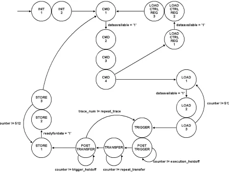
The Simple Circuit control state machine is shown in Figure 4.3. The hardware waits
next byte read in is written to the associated control register. If the command byte is0x05,
[image:45.612.83.551.138.492.2]the hardware waits for 512 data bytes to be transferred from the host computer.
Figure 4.3: Simple Circuit System Control State Diagram
Once the data is transferred from the host computer to the hardware, the state machine
immediately starts the data inverting process. First a trigger is sent out which lasts for
one clock cycle. Then the post-trigger wait lasts for the number of cycles specified in the
execution holdoff register. Then the transferstate is executed for the specified number of
cycles. This is where the data registers are inverted once per cycle. After the data inversion,
wait cycles are inserted during the post transfer state. Here the entire process can begin
can be used. Different scopes have different minimum requirements for trigger hold-off,
horizontal delay, and other parameters. One hardware design can support all of these. Also,
equivalent-time oscilloscopes require one trigger per each sample. The Simple Circuit
hardware can be configured to support this without having to pay the penalty for the UART
[image:46.612.92.528.198.490.2]communication each time.
Figure 4.4: Simple Circuit Top Level Testbench
In order to verify functionality and assist development, a testbench is used which
con-nects the Simple Circuit hardware to a model of a host computer with a UART. Data values
are read from an input file which contains the command bytes, control register values, and
data to be inverted. The resulting output data is written to an output file.
The baud rate of the UART is set to 9600 bits per second. In order to avoid this time
during simulation, some useful synthesizer directives are used. Figure 4.5 shows how the
directives are used. With these statements, different code is used between the simulation
and also to use only 4 data bytes instead of 512.
Figure 4.5: Useful Altera Synthesis Directives [18]
Hardware simulations are completed in ModelSim PE 6.3a. Figure 4.6 shows a
simu-lation waveform for the Simple Circuit hardware design. Note that only four data bytes are
being used. These bytes are inverted once per cycle during thetransferstate. The number
of cycles in each of the posttrigger, transfer, andposttransfer states are controlled by the
control registers.
Figure 4.6: Simple Circuit System Control Waveform
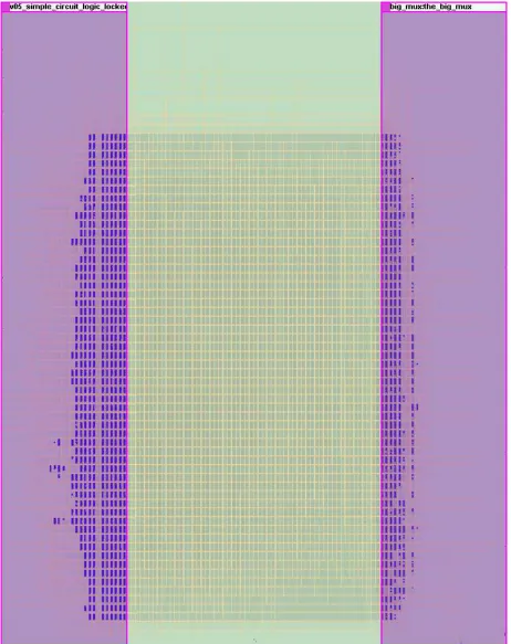
The most advanced Simple Circuit is the one which is Logic Locked. The Altera
Quar-tus II software allows hardware designs to be partitioned by entity. These partitions can
have either fixed or variable positions and/or size. When they are fixed, they are set by the
user and when they are variable, they are set by the Fitter. In order to maximize power
consumption, the third Simple Circuit Design was separated into partitions and locked into
either side of the FPGA. All of the data registers are locked on the left side of the chip. The
output multiplexer which is used to read the data back to the host computer is locked on
the right side of the chip.
This partitioning is shown in Figure 4.7. The output multiplexer is on the right side
and all other logic is on the left. The two pink rectangles are the design partitions. The
routing and the gold represents the global routing. The long routing channels between the
data registers and the output multiplexers will require more power to charge than shorter
local routing.
During each cycle of the transfer state, the data from the registers is inverted. That
means during each cycle, some data lines are being pulled high. However, the long routing
across the Logic Locked design are only charged when the output of the registers change
from logic zero to logic one. Therefore, the power consumption difference should be seen
every other cycle during thetransferstate. This is why the hardware is designed so that the
data bits which are inverted are written from the host computer. There they can be changed
to different proportions of active bits. This also keeps the synthesis tool from removing
the logic as unnecessary. The data is read back out for the same reason and to verify the
inversion.
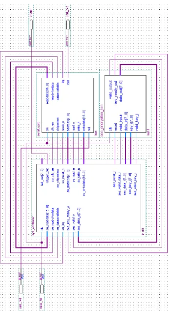
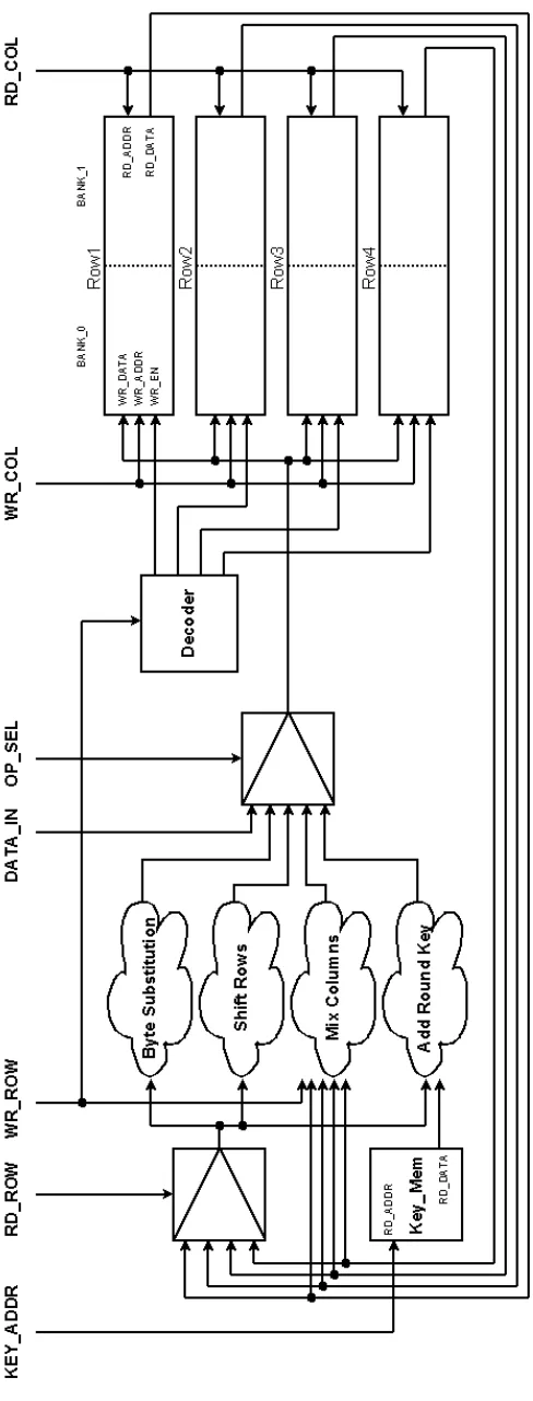
4.2 Custom Iterative
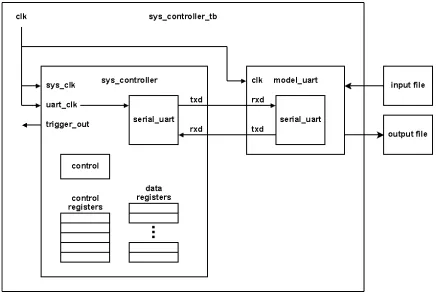
The Custom Iterative hardware design is a serial AES design. The design is constructed in
a structural manner. It is designed to encrypt with a 128-bit cipher key. Figure 4.8 shows
a system level diagram of the design. A serial RS-232 UART is used to communicate with
a host computer. The system controller block is used to maintain the control registers and
Figure
4.8:
Custom
Iterati
ve
System
Le
[image:50.612.125.471.67.703.2]When the system starts executing, it waits for a command which signals the start of a
plaintext transfer. When the controller receives the byte 0x02 over the UART, it will store
the next 16 bytes received into plaintext registers. Once all 16 plaintext bytes have been
stored into registers, the system begins the encryption. The system controller holds the
clock enable and chip select lines of the UART such that it does not operate during the
trigger, post-trigger wait, and encryption process. The UART is held inactive during this
time to avoid unnecessary noise on the power lines. The system control interface is the
same as that of the OpenCores.org AES Core Modules design.
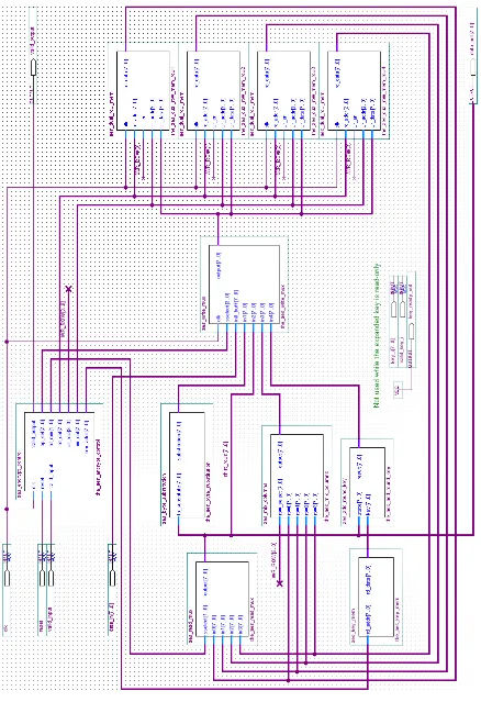
The design of the Custom Iterative AES hardware is also very structural. Figure 4.9
shows a top level diagram of the Custom Iterative AES design. There is a single entity
which acts exclusively as the control unit for the entire design. There are four identical
memory units named aes dual row mem. Each unit contains two banks which can each
store a row of the state matrix. Collectively, this memory is used to store the previous and
next state of the encryption.
The execution units for the four operations of AES are lined up and grouped together.
Theaes byte substitutionunit performs the non-linear inversion in the Galois FieldGF(28).
This is implemented as a look-up table. Since the shift rows operation changes only the
location and not the byte values in the encryption state, it is implemented as a direct
connec-tion. The control unit is programmed to reorder the bytes during this step of the encrypconnec-tion.
The bytes are simply read from a different location than they are written to between the two
row banks. The aes mix columns unit requires access to a byte in all four rows
simulta-neously. This is the motivation behind having a separate memory unit for each row of the
encryption state.
Theaes add round key unit is simply an XOR between an input byte of the state and
a byte of the cipher key or the round key. The aes round keyunit supplies the key bytes
Figure
4.9:
Custom
Iterati
ve
T
op
Le
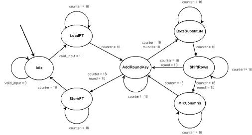
[image:52.612.93.531.72.711.2]The control state machine of the Custom Iterative AES design is shown in Figure 4.10.
The control unit coordinates the datapath elements to process one byte of the state matrix
[image:53.612.56.562.162.434.2]per cycle. Therefore, each AES encryption operation requires 16 clock cycles.
Figure 4.10: Custom Iterative State Diagram
After loading 16 bytes of plaintext into bank 0, the initial operation (AddRoundKey) is
performed over each byte in the state. Since the operation is independent between bytes in
the state, the input byte is replaced by the output byte in the same bank. Byte substitution
is performed in the same manner. The ShiftRows operation changes the location of the
bytes in each row. The encryption state data is transferred from bank 0 to bank 1 as this
happens. MixColumns also requires an independent copy of the input and output state data.
Therefore, MixColumns reads from bank 1 and writes the result into bank 0.
MixColumns is not performed in the final round of encryption. During this final round,
Figure
4.11:
Custom
Iterati
ve
[image:54.612.174.418.71.712.2]Figure 4.11 shows a simplified diagram of the Custom Iterative hardware datapath. One
important design decision is how to design the units which require memory. These units
include the state information, expanded key memory, and s-box ROM. The memory units
can be implemented with either registers or memory blocks. Memory blocks can either be
explicitly instantiated or the VHDL can be organized so that the synthesis tools can infer
memory blocks. Writing to memory is necessarily a synchronous operation. However,
reading can be implemented with either synchronous or asynchronous logic.
In order for the Altera Quartus II synthesis software to automatically infer memory, the
reading operations require registers on the inputs of the address lines [18]. This requires
that the read operation is synchronous. This slight memory difference significantly changes
the design and operation of the system controller. In order for the memory read interface to
be synchronous, the address lines must be available the cycle before the data is required for
computation. This adds significant complexity when working with three separate memory
units. It would also make it more difficult to determine what operation is taking place at
which time when the circuit is being used for power analysis. An implementation intending
to be optimized for throughput, latency, or area may implement the memory units in a
different way.
Therefore, all memory reads in the design are implemented as combinational reads. As
a consequence of this, all of the memory is implemented in registers on the target device.
In order to simplify the design, and since only a single key will be attacked at a time, the
expanded key is written into the key memory unit as a ROM. This expansion and VHDL
formatting is accomplished off-line in a Java software program.
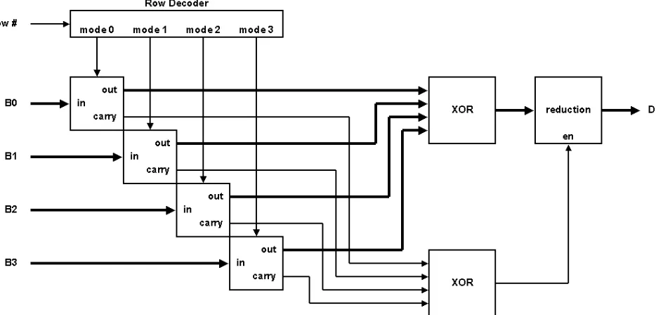
Custom Iterative Mix Columns Design
The most complicated part of the Custom Iterative architecture is the Mix Columns
oper-ation. This can be implemented in many different ways. The goal of the architecture is to
compute one byte at a time. In order to develop an architecture which performs in this way,
The main purpose of the Mix Columns operation is to vertically diffuse information
along each column in the AES state matrix. In order to accomplish this, each byte in a
column is considered a coefficient in a polynomial. This polynomial is then multiplied by
the constant polynomial3x2+x2+x+ 2. Table 4.2 shows how the bytes are read from the
first column of the state matrix [5].
The arithmetic is performed in the Galois Finite FieldGF(28). Therefore, addition is
simply an XOR operation. Multiplication is more complicated, but can be simplified since
the product of a number by a constant 1, 2, or 3 is all that is necessary.
b0 b1 b2 b3
Table 4.2: Mix Columns Byte Ordering
The column bytes represented as coefficients of a polynomial are multiplied by the
constant polynomial as shown in Equation 4.1.
b3x3 + b2x2 + b1x + b0
× 3x3 + x2 + x + 2
2b3x3 + 2b2x2 + 2b1x + 2b0
b3x4 + b2x3 + b1x2 + b0x
b3x5 + b2x4 + b1x3 + b0x2
3b3x6 + 3b2x5 + 3b1x4 + 3b0x3
(4.1)
The result must be four bytes represented as the coefficients of the variablesx3, x2, x1, x0.
Finite field arithmetic is used to reduce the variables with higher exponents by the
polyno-mialx4+ 1. This is accomplished with the following observation: ximod(x4+ 1) =ximod4
2b3x3 + 2b2x2 + 2b1x + 2b0
b2x3 + b1x2 + b0x + b3
b1x3 + b0x2 + b3x + b2
3b0x3 + 3b3x2 + 3b2x + 3b1
(4.2)
The output from this sum of products results in four bytes. The array can be reordered
such that each row corresponds to an output byte. Therefore, the first row corresponds to
the output byte associated withx0. The array can also be ordered such that each column is
associated with an input byte (b0, b1, b2, b3).
2b0 + 3b1 + b2 + b3
xb0 + 2xb1 + 3xb2 + xb3
x2b
0 + x2b1 + 2x2b2 + 3x2b3 3x3b
0 + x3b1 + x3b2 + 2x3b3
(4.3)
Then the sum of products can be represented by a matrix multiplication as in Equation
4.4. This is after the variables from the polynomial representation are removed. This
equation clearly shows how each byte in the next state column is based on every byte in the
current state column. This is how the vertical diffusion is performed.
2 3 1 1
1 2 3 1
1 1 2 3
3 1 1 2
· b0 b1 b2 b3 = d0 d1 d2 d3 (4.4)
The Custom Iterative design aims to calculate one output byte per cycle. From the
matrix multiplication representation, it is easy to see how each next state column byte
can be calculated by multiplying each current state column byte by either 1, 2, or 3 and
summing the products together.
A hardware design of these calculations with these goals can be represented as in Figure
row where the output byte will be placed. The output is the resulting byte representing the
sum of products of the input bytes.
The four identical components represent hardware units which multiply an input byte
by either 1, 2, or 3. This results in a product byte and a carry bit. The Row Decoder module
determines the constant each input byte is multiplied by.
Figure 4.12: Custom Iterative Mix Columns Mode Diagram
The resulting products and carry bits are summed together with XOR logic. If the sum
of the carry bits results in an active bit, the resulting byte must be reduced by the byte 0x1B.
This operation is simply a conditional addition (XOR).
row mode0 mode1 mode2 mode3
00 10 11 01 01
01 01 10 11 01
10 01 01 10 11
[image:58.612.87.554.207.431.2]11 11 01 01 10
Table 4.3: Custom Iterative Mode Decode
The combinational output from the Row Decoder is shown in Table 4.3. This is
inGF(28). The calculations are shown in Table 4.4 with VHDL notation. Multiplying by
two is simply a bit shift left. Multiplying by three is the same as multiplying by two with
an additional addition.
mode Meaning out carry
00 in·1 in 0
10 in·2 in(6 downto 0) & ’0’ in(7) 11 in·3 in(6 downto 0) & ’0’ xor in in(7)
Table 4.4: Custom Iterative Mix Columns Multiplication
Custom Iterative Performance
The serial design of this implementation causes the speed and throughput performance
measurements to be relatively low as compared to other AES implementations. The
com-plete encryption requires about 672 cycles as calculated in Equation 4.5. This calculation
assumes a simplification of 10 full rounds. This is equivalent to the actual implementation
since there is an initial transformation (Add Round Key) as well as a final round with the
Mix Columns operation missing.
total cycles=loadP T +rounds·(operations·16) +storeCT
total cycles= 16 + 10·(4·16) + 16
total cycles= 672cycles
(4.5)
The total resource utilization from the system level implementation as reported from
the Altera Quartus II Fitter is shown in Figure 4.13. A mor