Abstract—For the development of communication systems such as Internet of Things, integrating communication with power supplies is an attractive solution to reduce supply cost. This paper presents a novel method of power/signal Dual Modulation (PSDM), by which signal transmission is integrated with power conversion. This method takes advantage of the intrinsic ripple initiated in switch mode power supplies as signal carriers, by which a cost-effective communications can be realized. The principles of PSDM are discussed and two basic dual modulation methods (specifically PWM/FSK and PWM/PSK) are concluded. The key points of designing a PWM/FSK system, including topology selection, carrier shape and carrier frequency are discussed to provide theoretical guidelines. A practical signal modulation-demodulation method is given and a prototype system provides experimental results to verify the effectiveness of the proposed solution.
Index Terms— Power electronics, power line communication, power/signal dual modulation, pulse width modulation, distributed power system.
I. INTRODUCTION
n new concepts such as the Internet of Things [1-3] and the Industrial Internet [4-5], machine-to-machine communication is the backbone of future industrial and civil electrical systems, consequently is receiving extensive attention. A large number of smart „things‟ or „objects‟ including facilities, equipment, devices and sensors tend to be connected to future electrical systems, and the big data produced by them is transmitted, stored and analyzed [6]. This brings challenges to make these electrical systems more intelligent and reliable.
Manuscript received January 27, 2014; revised April 24, 2014; accepted June 13, 2014.
Copyright (c) 2014 IEEE. Personal use of this material is permitted. However, permission to use this material for any other purposes must be obtained from the IEEE by sending a request to [email protected].
This work is sponsored by the National Nature Science Foundation of China (61174157) and (51361130150).
J. Wu, J. Du, C. Zhao, and X. He are with the College of Electrical Engineering, Zhejiang University, Hangzhou 310027, China (e-mail: [email protected]; [email protected]; [email protected]; [email protected]).
Z. Lin is with the Electrical, Electronic and Power Engineering of the Aston University, Birmingham, U.K. (e-mail: [email protected]).
Y. Hu is with the Department of Electronic & Electrical Engineering, University of Strathclyde, Glasgow, UK. (e-mail: [email protected])
In most of traditional Distributed Control Systems (DCS), communication circuitry and power supply circuit are separately designed, so two independent circuits are needed. For example, in distributed power supply systems, additional communication circuits are added to receive control instructions from a supervisor controller or to exchange data between power converters [7-10]. On the other hand, for communication nodes in classic field bus systems, such as RS-485 or CAN, dedicated power converters are required to provide a stable power supply [11-12].
To simplify the wire connection of the system, two techniques are adopted [13-27]. The first technique is wireless communication, which has been widely used and increasingly accepted for industrial control systems [13-15]. However, due to the lack of physical protection, the security and reliability of wireless networks are often doubted, and other methods have been proposed for protection [16-17]. On the other hand, for most industrial systems, the nodes of wireless networks must be powered, so they inevitably connect with the power supply by wires. The second technique which simplifies connectivity is Power Line Communication (PLC), which originates from the so called second industrial revolution [18-20]. The idea of transmitting a signal on a battery powered cable was used in the London–Liverpool telegraph system, which was the earliest record of integrating the signal transmission through power cables [18]. Since the 1920‟s, the invention of carrier frequency transmission (CTS) and ripple carrier signaling (RCS) techniques has made PLC an option for remote load control. By the late twentieth century, with the development of integrated circuits and the Internet, considerable progress has been made in modulation methods and its application scope [19]. Nowadays, PLC techniques cover both the high voltage transmission networks and medium/low voltage distribution networks, which can supply services such as voice transmission, internet access, remote meter reading and load control, over the power cable. The PLC channel model has been comprehensively investigated [20-21], with numerous applications reported [22-27]. This technique has proved a reliable method for communication.
However, both wireless communication and PLC require independent circuits to amplify the communication signal. For PLC, extra inductive or capacitive coupling units are required to embed the data signal into the power line, which increases system costs and volume.
Power Conversion and Signal Transmission
Integration Method Based on Dual Modulation
of DC-DC Converters
Jiande Wu, Member, IEEE, Jin Du, Student Member, IEEE, Zhengyu Lin, Senior Member, IEEE, Yihua
Hu, Member, IEEE, Chongwen Zhao, Student Member and Xiangning He, Fellow, IEEE
In [28-29], the authors present a novel method that realizes power line communication between DC-DC converters which share a common input DC bus. Because the communication signal is inherently generated by the pulse width modulation of DC-DC converters, there is no need for an additional power amplifier to inject the signal on to the DC bus. This confirms the possibility of integrating communications into power conversion. However, these researchers mainly focus on signal processing, and the intrinsic relationships between the power electronic circuit and the communication model are not investigated.
This paper presents a power/signal dual modulation (PSDM) method to integrate data transmission with power conversion.
The communication model and the methods of
modulation/demodulation are analyzed in detail. The proposed technique of PSDM embeds a communication system into a power supply system, and is a cost-effective way to realize local communications for some power systems.
This paper is organized as follows. The PSDM principle is presented and analyzed in Section II. The applicable conditions, including topology choices and modulation methods are discussed in Section III. Modulation and demodulation methods are shown in Section IV. Prototype design and experimental verification are shown in Section V. Finally, conclusions are given in Section VI.
II. PRINCIPLE OF POWER/SIGNAL DUAL MODULATION
In power electronics, power converters are constructed with semiconductor switches and passive elements such as inductors and capacitors. Pulse width modulation (PWM) is the most popular strategy employed in the control of power converters. For the typical PWM waveform shown in Fig.1, the Fourier coefficients are
tT dT
V
T T
t f
Fig.1 A typical PWM waveform.
0
1 1
( ) ncos( ) nsin( )
n n
f t a a n t b n t
(1)0
a dV (2)
2
sin( ) cos(2 )
n
V
a nd n nd
n t
(3)
2
sin( ) sin(2 )
n
V
b nd n nd
n t
(4)
2 2 2
sin( )
n n n
V
c a b nd
n
(5)
where is the angular frequency of the waveform, d is the duty ratio associated with period T,t is the delay time ratio of the pulse, which corresponding to the angular component of the harmonics. For conventional pulse width modulated circuits, the duty cycle d of each period is controlled to achieve a given average voltage which corresponding to the DC component of equation (1). Although being filtered, the high frequency harmonic components, with initial amplitude represented by (5), still exist at the input and output ports.
For a PWM system there are three freedoms that can be manipulated. Except the duty cycle d used by PWM, the frequency f and phasetcan be modulated to carry information, which correspond to the Frequency-Shift Keying (FSK) and Phase-Shift Keying (PSK) modulation in signal communications. So that PWM/FSK or PWM/PSK dual modulation can be employed to simultaneously realize power conversion and signal transmission, which is also termed power/signal dual modulation (PSDM).
Power modulation
-+
Converter
PID
Data
Input Output
Driver
f1 f2 FSK modulation
Fig.2 Block diagram of PWM/FSK dual modulation.
T0
Driving Signal
t
t FSK modulated
carrier
„0‟ „1‟
[image:2.612.338.533.160.387.2]T1
Fig.3 Drive signal of PWM/FSK dual modulation.
This paper focuses on PWM/FSK modulation and does not pursue PWM/PSK. Fig.2 shows the block diagram of a PWM/FSK dual modulated system. Different from conventional PWM, the carrier of the PSDM system is a FSK regulated PWM signal. A PWM/FSK modulated waveform is shown in Fig.3, where the circuit operates at frequency f0 while
sending data „0‟, and frequency f1 while sending data „1‟. The
ripples in the input and output port waveforms carry information that has been modulated, on which a communication system depends.
III. APPLICABLE CONDITION AND COMMUNICATION MODELING
A. Structure of the PSDM system
Converter
Sending
Data Demodulate
Received Data
DC Bus
Signal path from PSE2 to PSE1 Path of Power transmitting
Signal path from PSE1 to PSE2
P
o
w
er
in
p
u
t
PSE1
P
o
w
er
o
u
tp
u
t/C
o
m
m
u
n
ic
at
io
n
c
h
an
n
el
Converter
Sending
Data Demodulate
Received Data
PSE2
P
o
w
er
in
p
u
t
[image:2.612.61.293.439.623.2]Converter
Sending Data Demodulate Received
Data DC Bus
Signal path from PD2 to PD1 PD2
Path of Power transmitting Signal path from
PD1 to PD2 Converter
P
o
w
er
in
p
u
t/C
o
m
m
u
n
ic
at
io
n
c
h
an
n
el
PD1 Pow
er
o
u
tp
u
t
P
o
w
er
o
u
tp
u
t
Sending Data Demodulate Received
Data
(b)Source splitting structure of a PSDM system. Fig. 4 Two basic structures of a PSDM system.
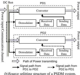
The basic structure of conventional distributed power systems includes paralleling, cascading, load splitting, source splitting and stacking [30], which are also available for power/signal dual modulation system. In this paper, we define two fundamental devices: Power Sourcing Equipment (PSE) and a Powered Device (PD). PSE is a converter that communicates at the output while PD is a converter that communicates at the input.
The structure of load splitting is shown in Fig.4(a) while source splitting is shown in Fig.4(b). The difference between these two structures is the channel of communication, source splitting lies in the input while load splitting lies in the output.
B. Topology analysis for PSDM
Theoretically, all switching mode DC-DC converters can create additional high frequency voltage signals at their input or output, which could be used as a signal carrier. The additional voltage signal in the converter port includes two components, switching noise and switching ripple. Switching noise is sensitive to circuit design and the placement of switching components, so is difficult to utilize. Switching ripple is the voltage generated by converter ripple current, and is stable when the circuit component values are determined. The voltage ripple equals the product of current ripple and port equivalent impedance.
For basic dc-dc topologies such as buck and boost converters, it is difficult to predict the current ripple amplitude if the circuit operates in a discontinuous conductive mode (DCM), because the current ripple is sensitive to the load. So in this paper, all analysis is based on synchronous rectification (bidirectional current flow) to prevent DCM.
To achieve reliable communications, the carrier should be stable in magnitude, but for some power electronic topologies, the ripple is vulnerable to the variation of input voltage and output load. Therefore, the applicable operating conditions of each dc-dc topology should be assessed.
In a buck converter (Fig.5), the input current is pulsative (always discontinuous) and its amplitude is determined by the load, which means that the signal carrier is unstable so the buck converter is unsuitable for a PSDM-PD device. However, the output current of the buck converter is continuous and the ripple amplitude (Δi=Uo(1-d)Ts /L) is load independent. The
basic harmonic amplitude of the output current ripple is
0 0
1 2 sin( ) ( ) 1max ( )
s s
U T U T
I d Sa d I Sa d
L
dL
(6)
where U0 is the output voltage, Ts is the period, L is inductance.
For a voltage regulated buck converter, assuming the input voltage varied from 1.3U0 to 3U0, the duty cycle d changes
from 0.33 to 0.77 while I1 varies from 0.83I1max to 0.27I1max,
which is acceptable for signal communication.
From this analysis, it can be concluded that the buck converter is suitable for PSE, but not for PD.
Similarly, the input current of boost converter is continuous, and the ripple magnitude (Δi=UddTs /L) is independent of load,
while its base frequency amplitude is
0
1 2 sin( ) 1max sin( )
s
U T
I d I d
L
(7)
For a voltage regulated boost converter if d varies from 0.3 to 0.7, the output ripple I1 changes from 0.81I1max to I1max.
However, the output current of a boost converter is pulsative, that is discontinuous. Therefore the boost converter is suitable for PD, but not PSE.
The discussion in following section is based on the boost converter, which operates as a PD.
L C Q1
Q2 R
Ud
iL id
0
dTS TS
t
0 dTS TS
t id
iL D
iL
U0
+
-Fig.5 Buck converter and its current ripple.
L C
Q1
Q2
R
Ud
iL
0 dTS TS
t
0 dTS TS
t iT
iL Di
L
+
-iT
[image:3.612.87.258.51.212.2]U0
Fig.6 Boost converter and its current ripple.
Extending the analysis to other dc-dc converter topologies, the applicable suitability conditions (continuous port current) can be obtained, as summarized in Table. I.
TABLE .I APPLICABILITY OF TOPOLOGIES
Converter topology PD PSE
Buck Unsuitable Suitable
Boost Suitable Unsuitable
Buck-Boost Unsuitable Unsuitable
Cuk Suitable Suitable
Sepic Suitable Unsuitable
Zeta Unsuitable Suitable
C. Shape of the modulated carrier
In a power/signal dual modulated converter, although power conversion and signal modulation are realized by a unified circuit, the control process of these two functions should be decoupled, which means the signal modulation should not affect the process of power conversion (and vice versa).
[image:3.612.327.543.306.489.2] [image:3.612.314.560.539.621.2]the switching frequency shifts from f1 to f2, the average current
is iAV1, and the peak to peak current ripple is iL1, then the current
at the frequency shifting point is
1 1 1
1
1 ( )
2 2
d
L s AV L AV
dU
i t i i i
Lf
D (8)
where Ud is the converter input voltage.
After the switching frequency shifts to f2, assuming the duty
cycle remains the same, the peak to peak current ripple is
2 2
d L
dU i
Lf
D , so the average current is
2 2 1
1 2
1 1 1
( ) ( )
2 2
d
AV L s L AV
dU
i i t i i
L f f
D (9)
The average current difference before and after frequency shifting is
2 1
1 2
1 1
( )
2 d AV AV AV
dU
i i i
L f f
D (10)
Because the average output current in one switching cycle is
iT(AV)=(1-d)iAV , the frequency shifting will produce a current
perturbation even if the duty cycle remains constant, as shown in Fig.7(a). Therefore, embedding FSK modulation with a sawtooth carrier will introduce additional interference, which should be avoided in the design of the PSDM system.
i L
us1
ur
f1 f2
ug
iAV
Di
t
t
t ts
(a) Sawtooth carrier
i L
us1
ur
f1 f2
ug
iAV
Di=0
t
t
t ts
[image:4.612.318.569.223.485.2](b) Triangle carrier
Fig.7 Waveformsof the Boost circuit employing different carrier.
In Fig.7(b), a triangle wave is employed as a carrier (producing double edge modulation). The switching frequency shifts from f1 to f2 to modulate the intended signal. When the
switching frequency is f1, the average current is iAV1, the peak to
peak current ripple is iL1. After the switching frequency shifts to
f2, the peak to peak current ripple is 2
2
D d
L
dU i
Lf , the
average output current in one switching cycle remains the same, as shown in Fig.7(b).
According to this analysis, it is concluded that a triangle wave is a better carrier option.
D. Communication model
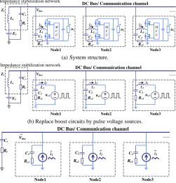
Take boost circuit as an example, Fig.8(a) shows a system composed of three nodes. Vbus is a common bus which is not
only for powering the node but also for data communication. E1
is a voltage source which supplies power to Vbus via an
impedance stabilization network Zr, which is comprised of a
LCR network. The function of the inductor Lr in the network is
to block the interference and impedance from the voltage source E1, where Lr complies with
1 2
2
r r
r
fL R
fC (11) where f is the switching frequency. The capacitor Cr in the
network is used to stabilize the bus, resistor Rr is the equivalent
series resistance (ESR) of Cr.
M C U
L1
……
Node1 Node2 Node3
C1
E1
i1 +
-Lr
Rr
Cr
u1 M
C U
L2
C2
i2 +
-u2
M C U
L3
C3
i3 +
-u3
Zr Vbus
DC Bus/ Communication channel Impedance stabilization network
Rs1 Rs2 Rs3
(a)System structure.
L1
……
Node1 Node2 Node3
C1
E1
i1
Lr
Rr
Cr
L2 C2
i2
L3 C3
i3
Zr Vbus
DC Bus/ Communication channel Impedance stabilization network
us1 us2 us3
Rs2 Rs3
Rs1
(b) Replace boost circuits by pulse voltage sources.
……
Node1 Node2 Node3
i1
Vbus
DC Bus/ Communication channel
C1 C2 C3
~
~
i2
~
i3
~ Rr
Cr
Rs1 Rs2 Rs3
(c) Simplified model for communication. Fig.8 Communication model of a boost-based system.
The equivalent series resistance of a boost converter input capacitor, represented by Rs1~3, cannot generally be ignored. In
steady state, the switch and output capacitor of the boost circuit is equivalent to a pulse voltage source from the point of view of signal communication (Fig.8 (b)).
Ignoring the dc component, the pulse voltage source and the inductor can be replaced by a triangle current source, so the diagram of the communication system is simplified to Fig.8(c). Without considering transmission line resistance, when n nodes are on the bus, the magnitude of the ripple voltage on Vbus is
~
~
1
1
( ) ( )
1 1
n k k
bus n
k r
r r k sk k
I j
V j
j C j C
j R C j R C
(12)
[image:4.612.104.240.336.558.2]IV. MODULATION AND DEMODULATION METHOD
All the nodes in a PSDM system produce noise signals if they do not send a data signal, which is different from traditional PLC techniques. Assume that the data carrier and noise are deployed in the same spectrum of the channel, according to the Shannon theory of channel capacity, the maximum communication rate C which a system can be realized is determined by
2
log (1 )
CB SNR (13) where B is the communication channel bandwidth and SNR is the signal to noise ratio. In a PSDM system of n nodes, assuming one node is sending and the others are waiting, the amplitude of either the signal or noise is equal, so the channel capacity of the bus can be express as
2 2
1 1.44
log (1 ) log (1 )
1
B
C B SNR B
n n
(14)
Equation (14) shows that the communication rate decreases as the number of nodes increases, on the condition any signal or noise is filtered without any discrimination. However, the equation (14) restriction can be overcome if a dedicate filter removes the noise frequency component.
In a binary frequency shift keying (BFSK) based PSDM system, two strategies can be utilized to transmit the data signal. The first is a three-carrier strategy: a carrier of frequency fnom is
adopted when a node is waiting for communication, carrier f0 is
applied as sending signal „0‟ and carrier f1 is applied as sending
signal „1‟, such that carriers shift between three frequencies. The second is a two-carrier strategy: carrier fnom is adopted
when waiting for sending data or sending signal „1‟, carrier f0 is
applied as sending signal „0‟. In this strategy, the carriers shift between two frequencies.
For a PSDM system, the carrier frequencies f0 and f1 should
be selected as close as possible to fnom to avoid adverse
converter effects, such as stability and filter designing problems. However, the closer the frequencies, the more difficult to differentiate them.
Assume that N nodes are on the bus and only one node is transmitting signal „0‟, the base frequency of the bus ripple is
1cos 2
nom 1
0cos 2
0 0
s t A f t A f t (15)
where A1 is the noise signal amplitude and A0 is the amplitude
of data signal „0‟. A1 is the synthesis of (N-1) waiting nodes and
the value is variable because the carrier phase in every node is different. Assuming in a period Ts, (15) is written as a complex
Fourier series:
2 /0
( ) j kt Ts
k
s t X k e
(16)To calculate the amplitude of the signal f0, it requires
0 0/ s 0 s
f m T m f (17) where m0 is an integer and fs is the Fourier transform frequency,
which means f0 is the m0th harmonic of the base frequency fs .
The amplitude of the signal f0 is
0
2 /
0 0 0
1
( ) s ( )
s
T j m t T
s
A X m s t e dt
T
(18)To eliminate the influence of frequency fnom , it should be
2 0/1
0 cos 2 0
s
s
T j m t T
nom
f t e dt
(19)It can be inferred that fnom should comply with
/ = ( is an integer)
nom n s n s n
f m T m f m (20)
This conclusion means that the noise and signal frequencies are different harmonics of the base frequency fs , which are
orthogonal in the Fourier transform period. Such a communication principle is often used in the techniques such as Orthogonal Frequency-division Multiplexing (OFDM) and Minimum Shift Keying (MSK).
To minimize the frequency difference of the signal and noise, it is assumed that mnm01, or
0
1 nom
S
f f f
T
(21)
If a three-carrier strategy is adopted, the frequency f1 should be
1
1 nom
S
f f f
T
(22)
In this paper, the two-carrier strategy is employed because the switching frequency difference is smaller than that with the three-carrier strategy. To guarantee the data communication transparency, the traditional byte-based serial communication method is adopted, which adds a „0‟ and „1‟ at the beginning and end of the byte, respectively.
In the receiver, ripple signals pass through a low-pass filter to remove high-order harmonics before it connects to an ADC channel of a DSP. The cut-off frequency fC of the low-pass
filter and the sampling time fsmp should comply with the
Nyquist theorem, or
2
smp C
f f (23)
Assume N is the sample number in a Fourier transform period and is specified by
smp S
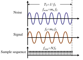
N f T (24) Fig.9 shows the relationship between sample frequency, noise frequency, and signal frequency.
Signal
Noise fnom=mnfS
TS=1/ fS
fsmp=NfS f0=m0fS
[image:5.612.361.521.453.569.2]Sample sequence
Fig.9 Waveforms of signal in a Fourier transform period.
The ripple signal sampled by the DSP is stored sequentially in memory, and then the DSP executes a discrete Fourier transformation (DFT) after each sample. The general DFT equation is
2 1
0
( ) ( ) ( 0,1,..., 1)
N j nk
N n
X k x n e k N
(25)Letting 0
2
j K
N e W
, the component of f0 is
1
0 0
( ) ( )
N
n K
n
X X K x n W
(26)x(2),…x(N)}, an iterative method of sliding DFT can be employed [31], and the new DFT value after the next sample can be expressed as
1
* 1
0 1
1
( 1) =( ( ) )
[ (0) ( )]
N N
n n
K
n n
K
X x n W x n W W
X x x N W
(27)Eqn.(27) decreases the DFT calculation time significantly, which makes it possible to execute the DSP DFT algorithm in every A/D sample period.
Assume that the effective signal received by each node is
0 0 0
( ) nomcos(2 nom n)[1 ( )] cos(2 ) ( )
x t A f t c t A f t c t
(28) where
1 (if sending bit '0') ( )
0 (no data or sending bit '1')
c t
The waveform shifts from fnom to f0 when c(t) changes from „1‟
to „0‟ at t0, and a window function g(t) is defined as 1 (0 )
( )
0 ( 0 or ) s
s
t T
g t
t t T
(29)
Assume the period of a bit is more than Ts, the result of
sliding sampling is x(t,t)
0 0 0
( , ) { cos(2 )[1 ( )]
cos(2 ) ( )} ( )
nom nom n
x t A f t c t
A f t c t g t
t
t
(30)
The f0 component of x(t,t) is
0
0
2
2 /
0 0 0
( ) ( , )
{ cos(2 )] ( )
cos(2 ) ( )}
t t t t
s sj f t K
T
nom nom n
j m t T
X x t e dt
A f t c t
A f t c t e dt
(31)
The amplitude of Xk(t) can be inferred
0
2 /
0 0 0
0 0
0
( ) [ cos(2 )
cos(2 )] ( )
0 if ( ) 0, (0 ) 2
( + )
2
( ) 1 (0 ) if
s
s
T
K nom nom n
j m t T
s
s nom
s n
X A f t
A f t c t e dt
c T
T A A
A
T m m
c t
t
t
t t
t t
0 0 0 0( ) 0 ( )
2
[ (1 )+ ]
2
( ) 0 (0 )
if
( ) 1 ( )
/ 2 if ( ) 1, (0 ) s s nom s n s s s c T
T A A
A
T m m
c
c T
A T c T
t t
t t
t t
t t (32)
According to (27), the DFT result is refreshed every sampling period. When the sliding window function g(t) coincides with the dedicated frequency f0, the result reaches a
maximum platform. Setting an appropriate threshold Xth or
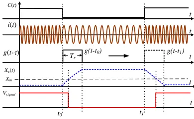
adopting more a complex judging algorithm, the data can be decoded. The process of demodulation is shown in Fig.10.
i(t)
Vsignal
C(t)
Xτ(t)
g(t-t) g(t-t1)
t
t
t
t
t
t0 t1
g(t-t0)
Xth
Ts
Fig.10 Schematic diagram of signal demodulation process.
V. EXPERIMENT VERIFICATION
A prototype system consisting five nodes is designed to verify the proposed method. The block diagram of the node is shown in Fig.11, which is based on conventional synchronic boost topology. The circuit is controlled by a DSP with related interface. The input current and output voltage are feedback for traditional close-loop control, and the ripple on the bus is filtered and amplified for signal decoding.
Vbus L1
[image:6.612.335.530.53.173.2]Filter And Amplifier Control Interface Load1 Current Sensing Cin C1 DSP TMS320F 28035 A/D Sample Dr iv er Ripple Sensing Output voltage PWM PWM Q1 Q2
Fig.11 Block diagram of a node.
The prototype system structure is the same as shown in Fig.8 (a), where nodes are connected to the bus which is powered by a DC voltage source via an impedance stabilization network. All the nodes can communicate with each other.
TABLE II.
SPECIFICATIONS OF PARAMETERS Parameter of the Boost circuit Value
Vbus (Input voltage) 10~15 V
Vout (Output voltage) 24 V
Pout (Maxim output power) 10W
L1 (Boost inductor) 560 μH
Cin (Input capacitors) 2.2 μF
Rs1 (ESR of Cin) 30m
fnom (Switching frequency) 100kHz f0 (Switching frequency) 83.3kHz Tsample (A/D sample period) 2s
ADC resolution 12-bit
DFT period 60s
Parameter of the Bus Value
n (Number of Nodes) 5
Line length 2m
Lr (Impedance Matching Inductor) 10μH Cr (Impedance Matching Capacitor) 2.2μF Rr (ESR of Capacitor Cr) 30m
[image:6.612.325.552.299.448.2]fnom=83.3kHz, and the discrete Fourier transform period is 60s
during which f0 and f1 are orthogonal to one another. It can be
calculated that m0=6 and mn=5. The DSP A/D sampling period
Tsample is 2s, so 30 words memory space is needed for DFT.
The transmission rate is 2kbps, to realize reliable communications.
0 0.1 0.2 0.3 0.4 0.5 0.6 0.7 0.8 -100
0 100
(ms)
(
m
V
)
0 0.5 1 1.5 2 2.5 3 3.5 4
-100 0 100
(ms)
(
m
V
)
0 0.5 1 1.5 2 2.5 3 3.5 4
0 50 100
(ms)
(
m
V
)
extended
fnom=100kHz f0=83.3kHz
Ripple
Ripple
Harmonic amplitude (f0=83.3kHz )
(a) One node installed on the bus.
0.5 0.6 0.7 0.8 0.9 1 1.1 1.2 1.3 -100
0 100
(ms)
(
m
V
)
0 0.5 1 1.5 2 2.5 3 3.5 4
-100 0 100
(ms)
(
m
V
)
0 0.5 1 1.5 2 2.5 3 3.5 4
0 20 40
(ms)
(
m
V
)
extended
fnom=100kHz f0=83.3kHz and fnom=100kHz
Ripple
Ripple
Harmonic amplitude (f0=83.3kHz )
(b)Two nodes installed on the bus.
0.5 0.6 0.7 0.8 0.9 1 1.1 1.2 1.3 -100
0 100
(ms)
(
m
V
)
0 0.5 1 1.5 2 2.5 3 3.5 4
-100 0 100
(ms)
(
m
V
)
0 0.5 1 1.5 2 2.5 3 3.5 4
0 10 20
(ms)
(
m
V
)
extended
fnom=100kHz f0=83.3kHz and fnom=100kHz
Ripple
Ripple
Harmonic amplitude (f0=83.3kHz )
[image:7.612.58.284.122.703.2](c) Five nodes installed on the bus.
Fig.12 Waveforms of ripple and the amplitude of the f0 harmonic.
In the receiver, a band-pass Op amp filter is designed to amplify the data signal and decrease the high harmonic
components, whose high-pass cut-off frequency is set about 150kHz. The output signal of the filter is about 1Vp-p and sampled by 12-bit ADC in the DSP TMS320F28035 every 2s. According to (27), the f0 (83.3kHz) component of the ripple is
on-line calculated by the DSP. TMS320F28035 has a CLA (Control Law Accelerator) core with 32-bit float-point math accelerator by which DFT algorithm is implemented in assembly language, and the calculation time is less than 1s.
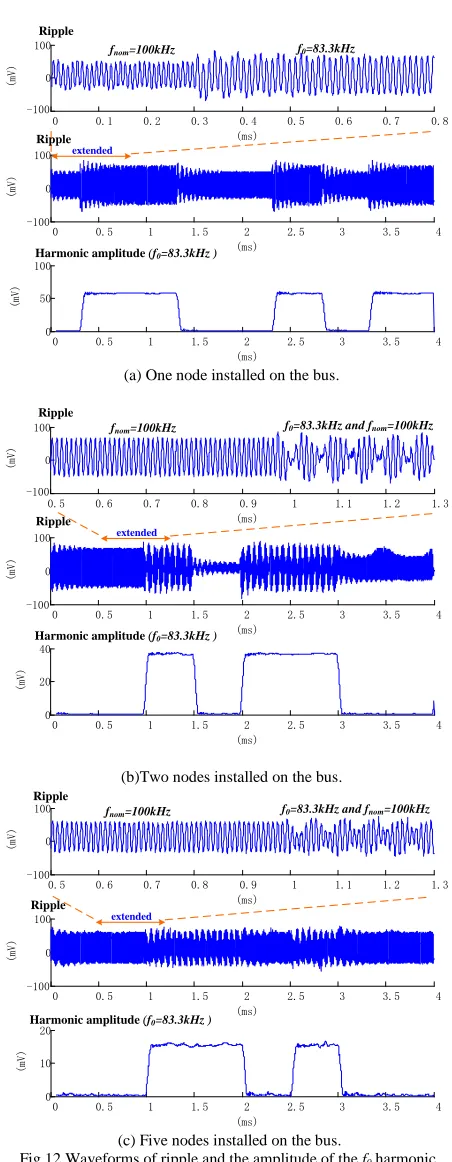
The ripple waveform of one node installed on the bus is shown in Fig.12(a), The ripple frequency shifts between 100kHz and 83.3kHz. In most cases, the node employs 100kHz switching frequency except when sending bit „0‟.
Fig.12(b) shows the ripple waveform and its DFT for two nodes operating on the bus, and Fig.12(c) shows the case for five nodes. If one node sends signal „0‟, the ripple on the bus is comprised of the components of f0 and fnom. The fnom (100kHz)
component on the bus is the synthesis of all nodes with different phases, so the amplitude is variable. However, the fnom
harmonic component will not affect the DFT result of f0
frequency in the DFT conversion period.
VSent
2V/div
VReceived
2V/div
200μs/div 1 0 0 1 0
Fig.13 Waveforms of sent data and received data.
From Fig.12, as the number of nodes increases, the amplitude of the f0 harmonic component reduces because the
bus impedance decreases. If a constant threshold XTh is set to
distinguish valid communication signal from noise, the condition that n nodes can be supported by this system is
n Th
V X (33) where Vn is the DFT result of the f0 component when n nodes
operate on the bus. The value of XTh is determined by the bus
noise which is related to the design of signal processing circuits and power control loop.
Assume the capacitance of all the input capacitor Ck
(k=1,2,…) in the nodes and the matching capacitor Cr are the
same, it can be concluded that the maximum number of the system is
1 max
2 1 Th
V N
X
(34)
where V1 is the DFT result of the f0 component when one node
operates on the bus.
[image:7.612.354.519.303.412.2]VI. CONCLUSIONS
This paper presents a method of power/signal dual modulation (PSDM) to integrate data transmission with power conversion. In the proposed PSDM system, the information is embedded into the ripple of the converter. By analyzing the waveform of the ripple, communication between nodes can be realized.
Two basic methods for PSDM are proposed, namely PWM/FSK and PWM/PSK. The modulation and demodulation process of PWM/FSK are discussed in detail and a prototype system is used to verify the technique. Two principles are concluded: firstly, topology and carrier may be constraints on the PSDM system. The boost converter circuit is suitable for PSE while the buck circuit is suitable for PD. A triangle wave is better carrier option since a sawtooth carrier introduces an additional interference problem. Secondly, the carrier frequencies should be orthogonal within a calculation period, and the difference of the shifting frequency is related to the communication rate. The closer the shifting frequencies, the slower communication rate.
This method proposes a way of designing an „intelligent power supply‟ which can send messages from the control core. The technique can be applied in distributed power systems or some special powering arrangements. However, some problems should be considered before use. First, the ripple utilized to communication should comply with EMI standards which restrict the amplitude of the harmonic frequencies; second, this method is not suitable for critical situations such as communication-based control systems; third, the effect of cross-interference between power control and signal transmission was not analyzed, and may cause communication data error, but this problem can be overcome by adding an Automatic Repeat Request (ARQ) mechanism into the communication protocol.
REFERENCES
[1] A. Iera, C. Floerkemeier, J. Mitsugi, and G. Morabito, “The Internet of things [Guest Editorial],” IEEE Wirel. Commun., vol.17, no.6, pp.8–9, Dec. 2010.
[2] E. I. Gaura, J. Brusey, M. Allen, R. Wilkins, D. Goldsmith, and R. Rednic, “Edge mining the Internet of things,” IEEE Sens. J., vol.13, no.10, pp.3816–3825, Oct.2013.
[3] D. Guinard, V. Trifa, S. Karnouskos, P. Spiess, and D. Savio, “ Interacting with the SOA-based Internet of things: discovery, query, selection, and on-demand provisioning of web services,” IEEE Trans. Services Comput., vol.3, no.3, pp.223–235, Jul.-Sept. 2010.
[4] Q. Wang, S. Gopalakrishnan, “Adapting a main-stream Internet switch architecture for multihop real-time industrial networks,” IEEE Trans. Ind. Inf., vol.6, no.3, pp.393–404, Aug.2010.
[5] A.C.Weaver, M.W. Condry, “Distributing Internet services to the network's edge,” IEEE Trans. Ind. Electron., vol.50, no.3, pp.404–411, June 2003.
[6] C. W. Thompson, “Smart devices and soft controllers,” IEEE Internet Computing, vol.9, no.1, pp.82–85, Jan.-Feb.2005.
[7] J. M. Guerrero, Lijun Hang, and J. Uceda, “Control of distributed uninterruptible power supply systems,” IEEE Trans. Ind. Electron.,vol.55, no.8, pp.2845–2859, Aug.2008.
[8] V. C. Gungor, D. Sahin, T. Kocak, S. Ergut,C. Buccella, C. Cecati, and G. P. Hancke, “A survey on smart grid potential applications and communication requirements,” IEEE Trans. Ind. Inf., vol.9, no.1,pp.28– 42, Feb.2013.
[9] S. K. Mazumder, M. Tahir, and K. Acharya, “Master–slave current-sharing control of a parallel DC–DC converter system over an RF
communication interface,” IEEE Trans. Ind. Electron., vol.55, no.1, pp.59–66, Jan. 2008.
[10] E. J. Bueno, A. Hernández, F. J. Rodríguez, C. Girón, R. Mateos, and S. Cóbreces, “A DSP and FPGA-based industrial control with high-speed communication interfaces for grid converters applied to distributed power generation systems,” IEEE Trans. Ind. Electron., vol.56, no.3, pp.654– 669, Mar.2009.
[11] T. Sauter, “The three generation of field-level networks-evolution and compatibility issues,” IEEE Trans. Ind. Electron., vol.57, no.11, pp.3585– 3595, Nov. 2010.
[12] B. Groza, and S. Murvay, “Efficient protocols for secure broadcast in controller area networks,” IEEE Trans. Ind. Inf., vol.9, no.4, pp.2034– 2042, Nov. 2013.
[13] A. Flammini, D. Marioli, E. Sisinni and A. Taroni, “Design and implementation of wireless fieldbus for plastic machineries,” IEEE Trans. Ind. Electron., vol.56, no.3, pp.747–755, Mar.2009.
[14] M., Sechilariu, B. Wang, F. Locment, “Building integrated photovoltaic system with energy storage and smart grid communication,” IEEE Trans. Ind. Electron.,vol. 60, no. 4,pp. 1607–1618, Apr. 2013
[15] Y. Ishii, “Exploiting backbone routing redundancy in industrial wireless system,” IEEE Trans. Ind. Electron., vol.56, no.10,pp.4288–4295, Oct.2009.
[16] E. M. Shakshuki, N. Kang, and T. R. Sheltami, “EAACK-A secure instruction-detection system for MANETs,” IEEE Trans. Ind. Electron.,vol.60, no.3,pp.1089–1098, Mar.2013.
[17] C. Alcaraz and J. Lopez, “A security analysis for wireless sensor mesh network in highly critical system,” IEEE Trans. Syst., Man, Cybern.C: Appl. Rev.,,vol.40, no.3,pp.419–428, Jul.2010.
[18] J.J. Fahie, “Edward Davy,” The Electrician, pp. 181–227, July, 1883. [19] T. A. Papadopoulos, C. G. Kaloudas, A. I. Chrysochos, and G. K.
Papagiannis, “Application of narrowband power-line communication in medium-voltage smart distribution grids,” IEEE Trans. Power. Del.,vol.28, no.2,pp.981–988, Apr.2013.
[20] H. Meng, S. Chen, Y. L. Guan, C. L. Law,P. L. So, E. Gunawan, and T. T. Lie, “A transmission line model for high-frequency power line communication channel,” in Proc. 5th Int. Conf. Power Syst. Technol., Kunming, China, Oct. 2002, vol. 2, pp. 1290–1295.
[21] M. A. Mannah, N. Ginot, and C. Batard, “Effect of the power cable on data transmission over a pulsewidth-modulated network,” IEEE Trans. Ind. Electron.,vol.61, no.8,pp.4238–4245, Aug, 2014.
[22] N. Pavlidou, A. J. Han Vinck,J. Yazdani, and B. Honary, “Power line communications: state of the art and future trends,” IEEE Commun. Mag., vol.41, no.4, pp34–40, Apr. 2003.
[23] V., K. Kilani, L. Koné, M. Liénard, and P. Degauque, “Feasibility of a high-bit-rate power-line communication between an inverter and a motor,” IEEE Trans. Ind. Electron.,vol.61, no.9, pp4816–4823, Sep., 2014. [24] T. Sauter and M. Lobashov, “End-to-End Communication Architecture
for Smart Grids,” IEEE Trans. Ind. Electron.,vol.58, no.4, pp1218–1228, Apr. 2011.
[25] J. Liu, B. Zhao, J. Wang,Y. Zhu, and J. Hu, “Application of power line communication in smart power Consumption,” in Proc. IEEE ISPLC, Mar. 2010, pp.303–307.
[26] H. Kubota, K. Suzuki, I. Kawakami,M. Sakugawa, and H. Kondo, “High frequency band dispersed-tone power line communication modem for networked appliances,” IEEE Trans. Consum. Electron., vol.52, no.1, pp. 44–50, Feb. 2006.
[27] C. Lin, H. Chu, S. Yeh,M. Lu, J. Yao, and H. Chen, “Robust video streaming over power lines,” in Proc. Int. Symp. Power Line Commun. Appl., Orlando, FL, 2006, pp196–201.
[28] W. Stefanutti, P. Mattavelli, S. Saggini, andL. Panseri, “Communication on power lines using frequency and duty-cycle modulation in digitally controlled DC-DC converters,” in Proc. IEEE IECON, Paris, France, 2006, pp.2144–2149.
[29] W. Stefanutti, S. Saggini, P. Mattavelli and M. Ghioni, “Power line communication in digitally controlled DC-DC converters using switching frequency modulation,” IEEE Trans. Ind. Electron., vol.55, no.4, pp.1509–1518, Apr. 2008.
[30] C.D.Xu andK.W.E.Cheng, “A survey of distributed power system - AC versus DC distributed power system,” in Proc. Conf. Power Electron. Syst Appl.,Hong Kong, 2011,pp.1–12.
Jiande Wu (M‟11)was born in Zhejiang, China, in 1973. He received the B.Sc., M.SC and Ph.D. degree from the College of Electrical Engineering, Zhejiang University, Hangzhou, China, in 1994, 1997 and 2012, respectively. Since 1997, he has been a faculty member at Zhejiang University, where he is currently an associate professor. From 2013 to 2014, he was an academic visitor at the University of Strathclyde, Glasgow, U.K. His research interests include power electronics control, distributed power electronics system and fieldbus communication.
Jin Du (S‟11) received the B.S. degree in electrical engineering from Zhejiang University, Hangzhou, China, in 2011. Currently, he is working toward the Ph.D. degree in the College of Electrical Engineering, Zhejiang University, China. His current research interests include power optimization of renewable generation and communication technique applied in power electronics.
Zhengyu Lin (S‟03–M‟05–SM‟10) received the B.Sc.and M.Sc. degrees from the College of Electrical Engineering, Zhejiang University, Hangzhou, China, in 1998 and 2001, respectively, and the Ph.D. degree from Heriot-Watt University, Edinburgh, U.K.,in 2005. He is currently a Lecturer in Electrical, Electronic and Power Engineering with Aston University, Birmingham, U.K. He was a Research Associate with the University of Sheffield from 2004 to 2006, an R&D Engineer with Emerson Industrial Automation, Control Techniques PLC from 2006 to 2011, a Senior Research Scientist with Sharp Laboratories of Europe Ltd. from 2011 to 2012, and a Lecturer with Coventry University from 2013 to 2014. His research interests include power electronics and its applications in renewable energy, energy storage, motor drives and power systems.
Yihua Hu (M‟13) received the B.S. degree in electrical motor drives in 2003, and the Ph.D. degree in power electronics and drives in 2011, both from China University of Mining and Technology, Jiangsu, China. Between 2011 and 2013, he was with the College of Electrical Engineering, Zhejiang University as a Postdoctoral Fellow. Between November 2012 and February 2013, he was an academic visiting scholar with the School of Electrical and Electronic Engineering, Newcastle University, Newcastle upon Tyne, UK. He is currently a research associate with the Department of Electronic & Electrical Engineering, University of Strathclyde, Glasgow, UK. He has published more than 20 technical papers in leading journals and conference proceedings. His research interests include PV generation system, DC-DC/DC-AC converters, and electrical motor drives.
Chongwen Zhao (S‟13) received the B.Sc. degree from the School of Electronic Engineering, Xidian University, Xi‟an, China, in 2011, and received the M.Sc. degree from the College of Electrical Engineering, Zhejiang University, Hangzhou, China, in 2014. Currently, he is working toward the Ph.D. degree in electrical engineering at the University of Tennessee, Knoxville, TN, USA. His research interests include wireless power and communication applications, DC-DC power conversions.