Implementation of Microcontroller Based
Controlling of Power Factor Using Capacitor Banks
Devanshu sharma1& Kuldeep panwar2 Department Electronics and computer science
ABSTRACT
Power factor correction (PFC) is a technique of counteracting the undesirable effects of electric loads that create a power factor that is less than one. Power factor correction may be applied either by an electrical power transmission utility to improve the stability and efficiency of the transmission network or correction may be installed by individual electrical customers to reduce the costs charged to them by their electricity supplier. Many control methods for the Power Factor Correction (PFC) have been proposed. This correction of power will be resolve by using PIC (peripheral interface controller) chip. Microcontroller-based developed algorithm to determine and trigger sufficient switching of Capacitors in order to compensate demand of excessive reactive power locally, thus bringing power factor near to unity.
Keywords—
Power factor correction (PFC); Electrical power transmission; Control method
I. INTRODUCTION
The power factor of an ac electric power system is defined as the ratio of the real power to the apparent power, and is a number between 0 and 1. Real power is the capacity of the electric load for performing work in a particular time. Apparent power is the product of the current and voltage of the electric load. Due to energy stored in the load and returned to the source, or due to a non-linear load that distorts the wave shape of the current drawn from the source, the apparent power can be greater than the real power. Low-
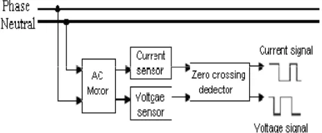
power-factor loads increase losses in a power distribution system and result in increased energy costs. Power factor correction is an old practice and different researchers are working hard to design and develop new system for the power factor correction. The principal element in the circuit is PIC microcontroller. The current and voltage single are acquired from the main AC line by using Current Transformer and Potential Transformer. These acquired signals are then pass on the zero crossing detectors. Bridge rectifier for both current and voltage signals transposes the analog signals to the digital signal. Microcontroller read the RMS value for voltage and current used in its algorithm to select the value of in demand capacitor for the load to correct the power factor and monitors the behaviour of the enduring load on the basis of current depleted by the load. In case of low power factor Microcontroller send out the signal to switching unit that will switch on the in demand value of capacitor. The tasks executed by the microcontroller for correcting the low power factor by selecting the in demand value capacitor and load monitoring are shown in LCD. [1]
II. ACPF
individually that transposed both current and voltage waveforms to square-wave to make perceivable to the Microcontroller to observe the zero crossing of current and voltage at the same time instant. In case of low power factor Microcontroller send out the signal to switching unit (relay) that will switch on the in demand value of capacitor. The tasks executed by the Microcontroller for correcting the low power factor by selecting the in demand value of capacitor and load monitoring are shown in Liquid Crystal Display (LCD).
III. ZERO CROSSING DETECTORS
The zero crossing detectors is a sine-wave to square-wave converter. The reference voltage in this case is set to zero. The output voltage waveform shows when and in what direction an Input signal crosses zero Volt. If input voltage is a low frequency signal, then output voltage will
be less quick to switch from one saturation point to another. And if there is noise in between the two input nodes, the output may fluctuate between positive and negative saturation voltage Vast. .Here IC 311 is used as a zero crossing detector the zero crossing detector is a sine-wave to square-wave Converter. The reference voltage in this case is set to zero. The output voltage waveform shows when and in what direction an Input signal crosses zero volt. If input voltage is a low frequency signal, then output voltage will be less quick to switch from one saturation point to another. And if there is noise in between the two input nodes, the output may fluctuate between positive and negative saturation voltage Vast. .Here IC 311 is used as a zero crossing
theoutput reduces to the saturation voltage of thetransistorwhich is nearly equal to zero Initially VBE = Cut-in voltage of diode, the capacitor will charge through the diode Vm where Vm is the maximum amplitude of the rectified wave.
FIG: Zero crossing detector
IV. ALGORITHM AND SIMULATION
In, this section we will discussed about the two major things of power factor correction using microcontroller are Algorithm and Simulation. So, we will first discussed the mathematical equations of power factor.
After the zero crossing of voltage and current Signals, which are converted to square-waves, are provided to Microcontroller. Power Factor is measured by the Microcontroller from manipulating of capture module for V and Isignals.
P = V(rms)I(rms)cosφ
For angle detection by taking the cos inverse of phi (φ) and getting the angle theta ( ).
Set the Phi (φ2) as a reference value equal to 0.9. And taking the cos inverse of 0.9 getting reference theta ( 1).
From the power angle diagram, the reactive power (VAR) utilized in circuit is given as:
tan 1 VAR =P×θ
For reference VAR tan2 VAR =P×θ
Required reactive power of the load is:
VAR =VAR1–VAR2
Current required for new VAR by load is: Irequired =VAR / Vrms
Required capacitor to improve the power factor for
Inductive load is given as:
Fig. 4 shows the flow chart of the proposed Automatic power factor controlling and load monitoring of the load. In the flow chart, the first step is about the Initializing the ACPF circuit. Microcontroller measures. The line voltage Vrms an Irms through ADC pins (AN0 andAN1) on real time basis. The voltage and current signals which have been converted into square waves after zero Crossing are provided to Microcontroller input pins (RC1And RC2) that are fundamentally the input of capture Module of the Microcontroller.
Now the simulation,
ACPF iscompletely based and tested on the simulation result are based on the lagging power factorof the load. Following are the simulations results whichincludes different cases of resistive and inductive load.
CASE 1: RESISTIVE LOAD
When resistive load is ON, as shown in Fig. There is no phase relay between current and voltage signals and they are in phase. In this case the power factor would be 0 .9 as referenced value so there is no insertion of capacitors In case of resistive load the V and I are in phase so there is no insertion of capacitors to improve power factor .The load monitoring of resistive load by microcontroller is shown on LCD.[4]
CASE 2: WHEN CHOCK (INDUCTIVE LOAD) IS ON:
There is phase delay between voltage and current signals, Microcontroller senses the Delay produced by the load, and according to the delay it inserts the desired value of capacitor to improve the power factor of the system. When the desired value of the capacitors added the required reactive power to the system, the current and voltage waveforms are in phase. After the insertion of required value of capacitor, the V and I zero cross detector signals are also in phase in accordance with the set referenced value of power factor (0.9).[5]
V. HARDWARE IMPLEMENTION
The controller operates on +5 V dc, so the regulated +v 5 v is supplied to pin no. 40 and ground at pin no. 20. The controller is used here need not required to handle high frequency signals, so as 4 MHz crystal is used for operating the processor. The pin no. 9 is supplied with a +5V dc through a push switch. To reset the Processor.First stage is concern with the step down. Arrangement of the incoming voltage and current signals into the PIC voltage level (e.g. 5V). Here we have used the step down arrangement of the transformer.
Second stage is concerned with zero crossing level detection by using an IC (LM358) for voltage and
current, the incoming signals. Voltage signal can be
acquired by using Opto-coupler (IC # 4N25) at the
output of Potential Transformer for detection. Current
signal can be acquired by using Current Transformer
Connected at main AC line. In third stage block diagram represents the Automatic power factor control with continuously load monitoring of the system as shown in Fig. 10, the main part of the circuit is Microcontroller (18F452) with crystal of 11MHz.
The main part of the circuit is Microcontroller (18F452) with crystal of Il MHz After acquiring voltage and current signals they are then passed through the zero cross detector block (ZCD V and ZCD l), that converts both voltage and current waveforms in square-wave that are further provided to microcontroller to detect the delay between both the signals at the same time instant. Two bridge rectifier circuits are utilized to convert both AC voltage and current signal into pulsating DC signal that is further provided to ADC pin of Microcontroller for its conversion into digital signal, so that the microcontroller performs Its further necessary task after this the
performed, these values are used in the algorithm of Microcontroller to select the Capacitor of desired value to counteract the effect of low power factor of the load and monitor continuously which load is operated on the basis of current consumed by the load. Results of corrected power factor, needed capacitor value to correct the low power factor to desired value are shown on LCD. [6]
Now the figure of hardware simulation of power factor control correction.
Results and Discussion
VI. CONCLUSION
It can be concluded that power factor correction Techniques can be applied to the industries, power systems and also households to make them stable and due to that the system becomes stable and efficiency of the system as
Well as the apparatus increases. The use of microcontroller reduces the costs. Due to use of microcontroller multiple parameters can be controlled and the use of extra hard wares such as timer, RAM, ROM and input output ports reduces. Care should be taken for overcorrection otherwise the voltage and current becomes more due to which the power system or machine becomes unstable and the life of capacitor banks reduces.
PIC monitors both continuously and then according to the lagging or leading power factor it takes the control action. This thesis gives more reliable and user friendly power factor controller. This thesis makes possible to store the real time action taken by the PIC microcontroller. This thesis also facilitates to monitor the power factor changes on LCD in real time.
REFERENCES
[1] Global Journal of Researches in Engineering Volume XIII Issue II Version I( ) Year F 2013
[2]Stephen, J. C. (1999). “Electric Machinery and Power System Fundamentals.” 3rdedition. United State of America: McGraw-Hill Companies, Inc.
[3]Bayindir R., Sagiroglu S., ColakI., An intelligent power factor corrector for power system using artificial neural Networks, ElectricPower Systems Research 79 (2009) 152– 160.
[4] International Journal of Engineering and Innovative Technology (IJEIT) Volume 3, Issue 4, October 2013
[5] International Journal of Engineering and Innovative Technology (IJEIT) Volume 3, Issue 4, October 2013
[6] PRZEGLĄD ELEKTROTECHNICZNY