Design and Characterization of Square Patch Salisbury Screen
Microwave Absorber
Amit Bhati1, *, Kirankumar R. Hiremath1, and Vivek Dixit2
Abstract—The work presents an inventive, simple and implementable design approach to enhance the bandwidth of conventional Salisbury Screen Microwave Absorber (SSMA). Theoretically, the maximum fractional bandwidth of SSMA for FR4 substrate with an optimum sheet resistivity of 308 Ω/sq for
−10 dB reflection is nearly 42.1%. In comparison, the bandwidth for square patch based SSMA is 59.7% with the same thickness. The design comprises square patches of SSMA placed periodically on a metal sheet. The square patches consist of an FR4 substrate and a 200 Ω/sq resistive sheet. A single reflection null is observed in the SSMA due to λ/4 resonance whereas in the proposed absorber an additional resonant mode is introduced due to coupling between the nearby patches. The simultaneous overlapping of the λ/4 mode and the additional coupling mode results in bandwidth extension. The close agreement between the simulation and measurement data is observed.
1. INTRODUCTION
The advancement of modern communication systems leads to complex electromagnetic environment. As a consequence, the problem of Electromagnetic Interference (EMI) arises which limits the applications of modern communication systems. It is essential to develop microwave absorbers to solve the EMI effectively. Additionally, they are required for radar signature suppression, improving antenna radiation pattern and minimizing the health risk by absorbing the unwanted radiations [1]. Microwave absorbers find huge potential in modern defence, civil and commercial systems.
The Salisbury and Jaumann absorbers are considered as classical microwave absorbers which have the disadvantages of narrow bandwidth with low angular stability and large size respectively [2, 3]. In material based absorbers, the absorption is due to imaginary parts of constitutive parameters viz. permittivity and permeability [4]. The material constitutive parameters can be tuned and physically realized by adding conducting fillers in epoxy resin [4]. The practical applications of the material based absorbers are limited by tailoring of constitutive parameters, thickness and complex synthesis process. In this context, Metamaterial Absorbers (MAs) are considered as novel microwave absorbers in terms of tuning resonant frequency, reduced thickness and nearly perfect absorption [5]. The MAs exhibit narrow bandwidth and act as polarization converter because of resonating structure and absence of resistive components respectively [5, 6].
Considering the limitations associated with different classes of microwave absorbers, it is essential to develop an alternative design approach to extend the bandwidth of existing microwave absorbers. The reported literature suggests that by introducing additional resonance modes lead to the bandwidth improvement viz. square patch based absorber and SSMA with wire metamaterial [7, 8].
This article presents a simple, novel and physically realizable design approach to enhance the bandwidth of conventional Salisbury Screen Microwave Absorber (SSMA). It is noticed that the bandwidth extension is achieved with a substrate of same thickness. The maximum fractional bandwidth
Received 24 March 2018, Accepted 25 April 2018, Scheduled 9 May 2018
* Corresponding author: Amit Bhati ([email protected]).
for SSMA using 3.2 mm thick FR4 substrate with optimum resistivity for−10 dB reflection is 4.7 GHz (8.8 GHz–13.5 GHz). In comparison to SSMA, the simulated and experimental bandwidth for −10 dB reflection is 8 GHz (9.4 GHz–17.4 GHz) for the proposed square patch based SSMA. The design comprises square patches of SSMA placed periodically on a metal plate. The square patches are physically realized on a 3.2 mm thick FR4 substrate with a 200 Ω/sq resistive sheet. The good agreement between the simulated and measured data supports the design methodology.
The commercial EM solver viz. CST Microwave Studio is employed to simulate theS-parameters of the absorbers using frequency domain solver under unit cell boundary conditions. The field quantities are numerically plotted as well to present the physical insight of the absorber. The performance of the absorber is analyzed for various angles of incidence under TE and TM modes. The absorbance of metal back absorber is represented byA= 1−R= 1− |S11|2.
2. DESIGN AND RESULTS
2.1. Salisbury Screen Microwave Absorber (SSMA)
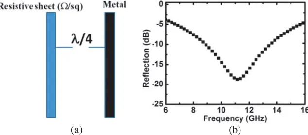
SSMA is a passive microwave absorber used for minimizing the backscatter from the metal. It is constructed of a resistive sheet placed λ/4 distance from the ground metal plate where λ is the wavelength in the medium (Fig. 1(a)). For λ/4 thickness, it forms an open microwave circuit which results in a single reflection null due to impedance matching condition [1].
(a) (b)
Figure 1. (a) Schematic of SSMA. (b) Simulated reflection from SSMA for d = 3.2 mm and Rs= 308 Ω/sq.
The detailed analysis of SSMA is reported in [2]. The optimized sheet resistivity and central frequency are expressed as:
Rs=Z0
1−ρρ∗ 1+ρρ∗
, fc=4dc√
where d and ε are the thickness and permittivity of the substrate respectively; Z0 is the free space
impedance;ρis the complex reflection coefficient. The optimized sheet resistivity for −10 dB reflection is 308 Ω/sq. The central frequency of SSMA can be tuned by either the thickness or the permittivity of the substrate.
2.2. Square Patch Based SSMA
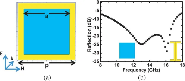
The enlarged top view of unit cell and simulated reflection of the proposed absorber are shown in Figs. 2(a) and (b), respectively. The unit cell consists of, bottom to top, metal plate, square patch of FR4 substrate with resistive sheet of 200 Ω/sq. The dimensions of unit cell are as p = 12 mm (periodicity), a = 10 mm (square patch size), d = 3.2 mm (thickness of FR4), and tres = 0.13 mm (thickness of resistive sheet). The permittivity and dielectric loss tangent of FR4 are 4.2 and 0.02, respectively. The simulated reflection indicates that the reflection is below−10 dB for frequency range 9.4 GHz to 17.4 GHz (Fig. 2(b)) with a bandwidth of 8 GHz. The total thickness of absorber is 3.33 mm.
(a) (b)
Figure 2. (a) Enlarged top view of proposed absorber along with field directions. (b) Simulated reflection for d= 3.2 mm,Rs= 200 Ω/sq, p= 12 mm and a= 10 mm.
3. ANALYSIS AND DISCUSSION 3.1. Square Patch Size Variation
Two reflection nulls are noted in the proposed absorber at 13 GHz and 16 GHz as shown in Fig. 2(b). The parametric analysis of patch size indicates that the minima corresponds to 13 GHz which is attributed to SSMA whereas the absorption peak at 16 GHz is due to capacitive coupling between the nearby square patches [10]. As the patch size increases, the reflection null (16 GHz) shifts towards lower frequency region due to increased capacitive coupling strength (Fig. 3(a)) [10]. For the given material, the coupling strength depends on patch size and spacing between the patches [9]. The square patches reduce the SSMA impedance which results in shifting of the SSMA absorbing peak (corresponding to 13 GHz) to higher frequency region (Fig. 3(a)). The two reflection nulls are selectively overlapped for a= 10 mm (square patch size) and result in 8 GHz bandwidth for−10 dB reflection (Fig. 2(b)). Fora= 12 mm =p, the space between the patches is zero which vanishes the coupling between the patches and results in the single resonant mode as observed in SSMA (Fig. 3(a)).
3.2. Oblique Angular Stability
The simulated reflections of the absorber for different angles of incidence are shown in Figs. 3(b) and 3(c) for TE and TM modes, respectively. The orientation of the absorber under TE and TM modes for different angle of incidence is discussed in [7]. The performance of the absorber under TE and TM modes is stable up to an angle of incidence 30◦ and normal incidence respectively. The less angular stability of the absorber under TM mode is attributed to variation in resistivity of the resistive sheet [2]. Multi-layer configurations are employed to achieve almost equal bandwidth under the two polarizations [2].
3.3. Physical Insight
(a) (b) (c)
Figure 3. (a) Simulated reflection for different patch size. (b) and (c) Simulated reflection for different angle of incidence TE and TM modes respectively.
(a) (b) (c) (d)
Figure 4. Simulated field quantities at 13 GHz and 16 GHz for p= 12 mm, a= 10 mm, d= 3.2 mm. (a) and (b) Electric field at 13 GHz and 16 GHz respectively. (c) and (d) Power loss density at 13 GHz at 16 GHz respectively.
at the edges of the square patches. The large electric field at edges indicates the presence of electric charges which leads to the formation of the capacitive feature. The power loss distribution at 13 GHz indicates that the maximum power loss is attributed to the resistive sheet, whereas at 16 GHz the power loss is confined to the edges of square patch. The field quantities support the origin of an additional resonance mode due to capacitive coupling between the patches.
4. FABRICATION AND MEASUREMENT
For demonstration purpose, the absorber is fabricated (Fig. 5(a)) with the dimension of 120×120× 3.33 mm. The FR4 sheet of thickness 3.2 mm with a resistive sheet with resistivity 200 Ω/sq is cut into 10×10 mm square patches manually. The patches are placed manually on a metal sheet with the periodicity of 12 mm, by epoxy based adhesive. The performance of absorber is measured in an anechoic chamber using VNA and a pair of horn antennas [7]. The good degree of correlation is observed between the simulated and measured data (Fig. 5(b)). The slight deviation is attributed to the nonuniform spacing between the patches due to manual alignment. The reflection from the absorber is measured for different aspect angles (−45◦ to 45◦) and compared with metal at 13 GHz (Fig. 5(c)). The absorber efficiently reduces the reflection in comparison to metal for every aspect angle [7]. The reduced reflection is attributed to absorption of the incident wave by the absorber. The performance of absorber is stable up to 30◦ for−10 dB reflection.
(a) (b) (c)
Figure 5. (a) Fabricated absorber. (b) Simulated and measured reflection. (c) Measured reflection from the metal and the absorber at 13 GHz for different aspect angles.
Table 1. Comparison with reported absorber.
Ref. Method Bandwidth GHz
(−10 dB reflection)
Thickness (mm)
Present work Square patch based Salisbury Screen 8 (9.4–17.4) 3.33
[11] Salisbury Screen with FSS 12 (4.6–16.6 ) 9
[12] Salisbury Screen of lossy
dielectric sheet (carbon nano fiber) 3.8 2.5
[13] Salisbury Screen with resistive loaded
high impedance ground plane 9 (4.7–13.7 ) 9
[14] Salisbury Screen with resistive FSS 10.4 (5–15.4) 7.6
5. CONCLUSION
The paper presents a simple, novel and physically implementable design methodology to enhance the bandwidth of Salisbury Screen Microwave Absorber using square patches. The bandwidth of the proposed absorber can be further improved by introducing additional resonances viz. designing a unit cell of different materials with varying thickness and sheet resistivity.
ACKNOWLEDGMENT
The first author is grateful to the Director, Defence Laboratory, Jodhpur, Rajasthan, India for kind permission to carry out the research work. The authors are thankful to Mr. R. K. Jani and Mr. Umesh Kumar of Defence Laboratory, Jodhpur, for their kind support in the characterization of the absorbers. The authors are as well thanks to Dr. Anuj Shukla of Defence Laboratory, regarding the resistive sheet. The efforts of Mr. Tejpal of Defence Laboratory, for cutting the FR4 sheet is acknowledged.
REFERENCES
1. Watts, C. M., X. Liu, and W. J. Padilla, “Metamaterial electromagnetic wave absorbers,” Adv. Mater., Vol. 24, OP98–OP120, 2012.
3. Saville, P., Review of Radar Absorbing Materials, Defence Research & Development Atlantic Dartmouth, Canada, 2005.
4. Qin, F. and C. Brosseau, “A review and analysis of microwave absorption in polymer composites filled with carbonaceous particles,” Journal of Applied Physics, Vol. 111, 061301, 2012.
5. Landy, N. I., S. Sajuyigbe, J. J. Mock, D. R. Smith, and W. J. Padilla, “Perfect metamaterial absorber”, Phys. Rev. Lett., Vol. 100, 207402, 2008.
6. Lin, B., B. Wang, W. Meng, X. Da, W. Li, Y. Fang, and Z. Zhu, “Dual-band high-efficiency polarization converter using an anisotropic metasurface,” Journal of Applied Physics, Vol. 119, 183103, 2016.
7. Bhati, A., K. R. Hiremath, and V. Dixit, “Square patch-based dielectric microwave absorber,”
Progress In Electromagnetics Research M, Vol. 63, 13–21, 2018.
8. Bhati, A., K. R. Hiremath, and V. Dixit, “Bandwidth enhancement of Salisbury screen micro-wave absorber using wire metamaterial,” Microw. Opt. Technol. Lett., Vol. 60, 891–897, 2018.
9. Luukkonen, O., F. Costa, C. R. Simovski, A. Monorchio, S. A. Tretyakov, “A thin electromagnetic absorber for wide incidence angles and both polarizations,” IEEE Transactions on Antennas and Propagation, Vol. 57, No. 10, 3119–3125, 2009.
10. Costa, F., A. Monorchio, and G. Manara, “Analysis and design of ultra thin electromagnetic absorbers comprising resistively loaded high impedance surfaces,”IEEE Transactions on Antennas and Propagation, Vol. 58, No. 5, 1551–1558, 2010.
11. Seman, F. C., R. Cahill, V. F. Fusco, and G. Goussetis, “Design of a Salisbury screen absorber using frequency selective surfaces to improve bandwidth and angular stability performance,”IET Microwaves, Antennas &Propagation, Vol. 5, No. 2, 149–156, 2011.
12. Kim, J. B. and J. H. Byun, “Salisbury screen absorbers of dielectric lossy sheets of carbon nanocomposite laminates,” IEEE Transactions on Electromagnetic Compatibility, Vol. 54, No. 1, 37–42, 2012.
13. Seman, F. C., R. Cahill, and V. Fusco, “Performance enhancement of Salisbury screen absorber using a resistively loaded high impedance ground plane,” Proceedings of the Fourth European Conference on Antennas and Propagation, IEEE, 2010.