Insertable Waveguide Verification Standards for the Electromagnetic
Characterization of Materials
Jonathan L. Frasch1, Edward J. Rothwell2, *, Premjeet Chahal2, and John Doroshewitz2
Abstract—A process is introduced to design and validate insertable rectangular-waveguide verification standards for the electromagnetic characterization of materials using the Nicolson-Ross-Weir method. Each insertable structure consists of a series of metal steps that acts as a surrogate material exhibiting smooth and predictable permittivity and permeability characteristics across the waveguide band. These known material properties can be used to assess the performance of material characterization systems. Since the verification standards are inserted into the waveguide in the same manner as samples under test, each step in the normal measurement procedure is duplicated. A specific example of an S-band verification standard is presented, with the standard fabricated using two different methods. The first standard is machined from a solid metal block while the second is constructed by metalizing a 3D printed polymer structure. Comparison of the predicted material parameters to those extracted from experimental data demonstrates the utility of the proposed insertable standards.
1. INTRODUCTION
The demand for novel materials for use in radio frequency (RF) systems has led to the introduction of a variety of artificial and engineered materials [1]. These include exotic constructions using graphene nanoribbons [2] and polymer ceramics [3]. A particularly important application of composite materials is for the construction of EMI shielding [4] and microwave absorbers [5,6]. These materials exhibit both magnetic and dielectric loss. Similarly, new techniques for miniaturizing RF components require that a material have both magnetic and dielectric properties [7]. The electromagnetic properties of all these materials are difficult to predict with any accuracy, due to modeling uncertainties and variabilities in the manufacturing process. Thus, the permittivity and permeability of engineered materials are generally determined through laboratory measurements.
One widely used technique for measuring both the permittivity and permeability of material samples is the rectangular waveguide method [8–10]. A block of material is inserted into a rectangular waveguide so that it occupies the entire cross-section and measurements of the reflection and transmission S -parameters are made. The Nicolson-Ross-Weir (NRW) method is then used to find the complex values of the permittivity, = 0(r −jr), and the permeability, μ = μ0(μr −jμr), from closed-form expressions [11, 12]. The rectangular waveguide technique has advantages over such alternative methods as free-space systems, including high signal strength, simplicity of sample preparation, and accurate knowledge of the applied field.
Rectangular waveguide measurement techniques have been developed over a period of years by the National Institute of Standards and Technology (NIST) [13,14] and are codified by ASTM International (originally the American Society for Testing and Materials) under the standard ASTM D5568 [15]. An important step in the D5568 procedure is the verification of system calibration using a known sample
Received 13 November 2017, Accepted 10 February 2018, Scheduled 3 April 2018
* Corresponding author: Edward J. Rothwell ([email protected]).
of material. The known sample is placed into the guide in the same manner as the unknown sample, and the S-parameters are measured. The properties of the verification sample are then extracted and compared to the known properties of the material. If the comparison is sufficiently close, the system may be used with confidence. If not, both the system and the process are inspected for errors. The D5568 standard suggests the use of RexoliteR (cross-linked polystyrene) or TeflonR (polytetrafluoroethylene). These plastics are highly stable, and have well-characterized values of permittivity. In fact, Rexolite and Teflon are used as verification standards in a wide variety of material measurement systems [16–20]. While plastic verification standards are highly useful for characterizing dielectric materials, no equivalent magnetic materials exist for characterizing materials with both dielectric and magnetic properties. Materials with significant magnetic properties at microwave frequencies have characteristics that are difficult to reproduce in a reliable manner. Since these materials usually consist of magnetic particles dispersed within a polymer matrix, there is significant variability between samples, and materials with highly predictable properties cannot be reproduced reliably. Therefore, there is a need for a surrogate material sample that can be constructed with high accuracy, having the equivalent magnetic properties of typical microwave materials when characterized using the NRW method.
Recently, an all-metal material surrogate was proposed by Crowgey et al. [21] that can be duplicated with high precision using normal machining techniques. When characterized using the NRW method, the surrogate produces properties similar to those of typical magnetic materials and thus can be used to verify the proper performance of the measurement system. However, since the structure is assembled from several stacked waveguide irises, the procedure used to validate the measurement system is not the same as that used to measure the properties of sample materials. In this paper, a new waveguide surrogate material is proposed that can be inserted into the waveguide in the same manner as the sample under test, thus producing a verification procedure identical to the normal measurement procedure.
The proposed material surrogate is a solid metallic block that fills the waveguide horizontally, but not vertically. A specified number of slots are machined into the block producing a structure with vertical steps that can be easily analyzed using mode matching. By using a genetic algorithm (GA), the heights and widths of the slots are chosen so that the equivalent material parameters, when extracted using the NRW method, are smooth and slowly changing across the measurement band, and best match those of specified target values.
An additional benefit of the proposed material surrogate is that it is smaller and can be made lighter than the solid blocks of dielectric that are currently used as verification standards. Many organizations use large waveguides, such as WR-1800, to measure material properties in the low microwave and UHF bands. Samples are cumbersome to maneuver and difficult to insert into large waveguides (often mallets must be used to force the samples in, so as to reduce air gaps). The solid metal surrogate may be hollowed out to reduce its weight, and the 3-D printed standard is inherently much lighter than a full-size sample. Ease of insertion significantly reduces the labor required for verification. As an example, a Rexolite verification sample for WR-1800 waveguide (457.2 by 228.6 mm cross-section) has a volume of approximately 12,000 cm3 and a mass of over 17 kg. In comparison, an aluminum verification standard based on the design described below (and hollowed slightly) has a mass of only 2.6 kg.
The procedure for designing the proposed verification standard is outlined, and a design for S-band waveguide is described. Measurements of two standards, one fabricated through a conventional machining process and one by 3D printing and electroplating, are provided for the design. Excellent agreement between the measured material parameters and those predicted by analysis validates using these standards for verification purposes.
2. DESIGN REQUIREMENTS AND PROCEDURE
can also be easily analyzed using standard mode-matching approaches [21]. To reduce the complexity of the problem, and to produce a structure that mimics the symmetry of actual samples, the steps are specified as mirrored pairs, resulting in S11=S22.
In addition to the symmetry requirement, the following constraints are applied to the designs:
(i) The height of the waveguide is discretized into NH identical values of height ΔH, and the vertical dimension of each section is chosen as a multiple of ΔH. The maximum allowed height is (NH−1)ΔH while the minimum allowed height is ΔH. This ensures that the structure does not block the waveguide completely and that it may be machined as one continuous piece.
(ii) The length of the surrogate is chosen such that the logarithm function used in the NRW method to extract the material parameters occupies a single Riemann surface for the entire frequency band. This prevents the discontinuous jumps in permittivity and permeability that occur when the surface boundaries are crossed as frequency changes.
It is important to carefully consider the number of sections and discretized heights to use. Allowing larger values of NL and NH produces greater design flexibility, but also creates a much larger search space for the GA to explore. A well designed GA will navigate the solution space toward optimal points, but it can take significantly more time to find better designs if the problem is very large. For the designs presented in this paper, which have relatively few sections, only a few generations were required to converge to an acceptable design. The actual time required to determine a typical design was approximately 1–2 hours of computer time using a 3.7 GHz Intel Core i7-4820K CPU with 64 GB of RAM. Also, since the length of the surrogate is restricted by the Riemann surface requirement, the use of a large number of sections introduces manufacturing difficulties. For higher-frequency waveguide bands the sections become narrow, and deformation from stress relaxation can occur in machined structures. The GA fitness function is constructed by using the theoreticalS-parameters, as determined from mode matching, to compute values ofand µwith the NRW method. The difference between extracted values of permittivity and permeability and target values specified by the designer is computed and a fitness bonus is assigned based on the variation of the extracted parameters across the frequency band (with the goal to produce parameters as frequency-independent as possible).
3. FABRICATION AND TESTING OF A BRASS WR-284 STANDARD
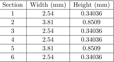
As a specific example, a verification standard was designed for an S-Band, WR-284 waveguide of width 2.84 inch (72.14 mm) and height 1.34 inch (34.04 mm), covering an operating band of 2.6-3.95 GHz. The structure is 0.7 inch (17.78 mm) long and is divided into six sections, alternating between 0.1 inch (2.54 mm) and 0.15 inch (3.81 mm) in length, as shown in Table 1. Each section was discretized into NH = 20 heights of ΔH = 0.067 inch (1.7018 mm). A target permittivity of 6−j0 and permeability of 6−j0 were chosen because of their interest to the end user. Note that by assuming the metallic structure to be perfectly conducting, the imaginary parts of µ and either are zero, or have opposite signs [23]. Since positive imaginary parts are unphysical, the imaginary parts of the target parameters were set to zero.
The GA was run to determine the heights of the sections. Several adequate results were obtained, with the dimensions of the one most amenable to fabrication described in Table 1.
Table 1. Dimensions of the tested WR 284 standard.
Section Width (mm) Height (mm)
1 2.54 0.34036
2 3.81 0.8509
3 2.54 0.34036
4 2.54 0.34036
5 3.81 0.8509
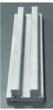
Figure 1. Brass WR-284 verification standard. Figure 2. WR-284 waveguide sample holder with verification standard in place.
-1 0 1 2 3 4 5 6 7
2.5 3 3.5 4
Relative Permittivity
Frequency (GHz) Measured Theory
Figure 3. Relative permittivity of the brass WR-284 verification standard.
-0.02 0 0.02 0.04 0.06 0.08
2.5 3 3.5 4
Relative Permittivity
Frequency (GHz) Standard Deviation Deviation from Theory
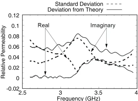
Figure 4. Measurement error and standard deviation of the measured permittivity for the brass WR-284 verification standard.
The verification standard described in Table 1 was machined from brass stock; the fabricated structure is shown in Figure 1. Note that this particular standard has a very low profile and thus is lightweight and easy to machine. Figure 2 shows the sample holder with the standard in place. Use of a NanoMap-500LS Contact Surface Profilometer over 12.7 mm of the top surface of the standard, with a data resolution of 1.3µm, revealed a standard deviation of the surface elevation to be 1.3139µm. The sample was measured using an Agilent E5071C network analyzer with two coaxial-to-waveguide transitions attached to two 5 inch (127 mm) waveguide extensions. Calibration was carried out using the TRL procedure and a 1.1875 inch (30.1625 mm) sample holder was placed between the waveguide extensions. The verification standard was then placed into the sample holder with its front face flush with the calibration plane of port 1. Deembedding was used to obtain the scattering parameters referenced to the front and rear faces of the verification standard.
-1 0 1 2 3 4 5 6 7 8 9 10
2.5 3 3.5 4
Relative Permeability
Frequency (GHz) Measured Theory
Figure 5. Relative permeability of the brass WR-284 verification standard.
-0.02 0 0.02 0.04 0.06 0.08
2.5 3 3.5 4
Relative Permeability
Frequency (GHz) Standard Deviation Deviation from Theory
Figure 6. Measurement error and standard deviation of the measured permeability for the brass WR-284 verification standard.
nonzero imaginary parts of µ and could be due to the loss in the brass, or to a slight asymmetry of the fabricated structure. As described in [23], only when the structure is lossless and S11 = S22 will the extracted material parameters have zero imaginary part across the band. Even so, since the sample standard deviations are very small, measurement of the waveguide standard can be repeated with high reliability.
4. FABRICATION AND TESTING OF A 3D-PRINTED WR-284 STANDARD
Three-dimensional printing is proved to be an affordable technology for fabricating waveguide components [24]. The part is printed as a polymer object and then sputtered or electroplated with a metal coating. Care must be taken to ensure that the thickness of the metal coating is significantly larger than a skin depth for the frequencies of operation. In the case of S-band, one skin depth of copper is approximately 1.3 microns.
A duplicate of the brass WR-284 verification standard described in the previous section was printed using an Objet Connex350 printer and VeroWhite material. Two small holes were printed into the part to allow electroplating wires to be inserted. After printing, the part was sputter coated with a 300 nm layer of titanium followed by a 1 micron layer of copper. The part was then electroplated with approximately 5 microns of copper to achieve a coating much thicker than a skin depth. Use of a NanoMap-500LS Contact Surface Profilometer over 12.7 mm of the top surface of the standard, with a data resolution of 1.3µm, revealed a standard deviation of the surface elevation to be 2.8396µm. The fabricated part is shown in Figure 7.
Figure 7. 3-D printed WR-284 verification standard with copper electroplating.
-1 0 1 2 3 4 5 6 7
2.5 3 3.5 4
Relative Permittivity
Frequency (GHz) Measured Theory
Figure 8. Relative permittivity of the 3-D-printed WR-284 verification standard.
-0.02 0 0.02 0.04 0.06 0.08 0.1 0.12 0.14
2.5 3 3.5 4
Relative Permittivity
Frequency (GHz) Standard Deviation Deviation from Theory
Figure 9. Measurement error and standard deviation of the measured permittivity for the 3-D-printed WR-284 verification standard.
5. 3-D MANUFACTURING OF PROPOSED VERIFICATION STANDARDS FOR HIGHER FREQUENCY MEASUREMENTS
The weight benefit of 3-D printed verification standards over those constructed using classical machining techniques is most obvious at lower frequencies where sample size can be quite large. At higher frequencies, the advantages of ease of construction and low cost remain. It is useful to consider the current technological limits that determine the upper frequency range of 3-D printed verification standards.
-1 0 1 2 3 4 5 6 7 8 9 10
2.5 3 3.5 4
Relative Permeability
Frequency (GHz) Measured Theory
Figure 10. Relative permeability of the 3-D-printed WR-284 verification standard.
-0.02 0 0.02 0.04 0.06 0.08 0.1 0.12
2.5 3 3.5 4
Relative Permeability
Frequency (GHz) Standard Deviation Deviation from Theory
Figure 11. Measurement error and standard deviation of the measured permeability for the 3-D-printed WR-284 verification standard.
solutions or thermoplastic melts, have been successfully adopted for the printing of high-resolution parts with a smooth surface.
Printed plastic components followed by electroless copper plating (with thickness greater than 5 skin depths) have been used to demonstrate metal waveguides working in the millimeter wave and terahertz (THz) frequency range [24, 25]. It is shown that a print resolution of less than λ/50 is needed to achieve low losses in waveguides. For this paper, a polyjet process was used to fabricate the verification standards using a commercial system, Objet Connex350. In this process, droplets of photosensitive polymer material are selectively deposited and cross-linked using ultraviolet light. This approach provides a print resolution as high as 16µm (or better than 25µm with good repeatability over a large area) and with surface roughness less than 4µm. Thus, it is possible to print waveguide components working in the millimeter wave range using this technology. The verification standards described in this paper were printed with tight tolerances, and the surface roughness was reduced below 2µm by mechanical polishing before copper deposition.
6. CONCLUSIONS
A process has been presented to design and evaluate waveguide standards for verifying the electric and magnetic properties of materials that are extracted using the Nicolson-Ross-Weir method. Each standard consists of a slotted metallic block that is inserted into the waveguide in the same manner as actual sample materials. Thus, the steps used in the verification process mimic the steps taken to measure a sample under test. Because the verification standards are made of metal, they can be machined to high accuracy, and are thus highly repeatable.
An S-band waveguide example is presented using two methods of fabrication. The design was determined by using a genetic algorithm to match the extracted parameters found from theoretical mode-matching data to chosen target values. The material parameters extracted from measurements of the fabricated standards match well with those determined from theoretical data, and the relatively small standard deviations from repeated measurements demonstrate that consistent and repeatable results may be obtained using simple construction methods, such as machining or 3-D printing.
oxidation, a small coating of a non-reactive metal such as gold might be used to protect the standard. As 3-D printing processes are improved, it is expected that the manufacturing tolerances will become comparable to more mature manufacturing techniques, and that direct 3-D printing of metallic parts may become affordable.
ACKNOWLEDGMENT
The authors greatly appreciate the generous support provided by Livingston Tool Mfg. throughout this project. They are also grateful to Brian Wright of the MSU ECE Department technical staff who provided assistance with 3-D printing and electroplating.
REFERENCES
1. Volakis, J. L. and G. Kiziltas, “Novel materials for RF devices,” 2007 IEEE Antennas and Propagation Society International Symposium, 1701–1704, Honolulu, HI, 2007.
2. Dimiev, A., W. Lu, K. Zeller, B. Crowgey, L. C. Kempel, and J. M. Tour, “Low-loss, high-permittivity composites made from graphene nanoribbons,” ACS Appl. Mater. Interfaces, Vol. 3, No. 12, 4657–4661, 2011.
3. Koulouridis, S., G. Kiziltas, Y. Zhou, D. Hansford, and J. L. Volakis, “Polymer ceramic composites for microwave applications: Fabrication and performance assessment,” IEEE Trans. Microwave Theory and Techniques, Vol. 54, No. 12, 4202–4208, 2006.
4. Verma, A., A. K. Saxena, and D. C. Dube, “Microwave permittivity and permeability of ferrite-polymer thick films,”J. Magn. Magn. Mater., Vol. 263, 228–234, 2003.
5. Vinoy, K. J. and R. M. Jha, Radar Absorbing Materials: From Theory to Design and Characterization, Kluwer Academic, Boston, MA, USA, 1996.
6. Feng, Y. B., T. Qiu, and C. Y. Shen, “Absorbing properties and structural design of microwave absorbers based on carbonyl iron and barium ferrite,” J. Magn. Magn. Mater., Vol. 318, 8–13, 2007.
7. Shirakata, Y., N. Hidaka, M. Ishitsuka, A. Teramoto, and T. Ohmi, “High permeability and low loss Ni-Fe composite material for high-frequency applications,”IEEE Trans. Magn., Vol. 44, No. 9, 2100–2106, 2008.
8. Chen, L. F., C. K. Ong, C. P. Neo, V. V. Varadan, and V. K. Varadan, Microwave Electronics: Measurement and Materials Characterization, Wiley, London, UK, 2004.
9. Ball, J. A. R. and B. Horsfield, “Resolving ambiguity in broadband waveguide permittivity measurements on moist materials,” IEEE Trans. Instrum. Meas., Vol. 47, No. 2, 390–392, 1998. 10. Larsson, C., D. Sj¨oberg, and L. Elmkvist, “Waveguide measurements of the permittivity and
permeability at temperatures of up to 1000◦C,” IEEE Trans. Instrum. Meas., Vol. 60, No. 8, 2872–2880, 2011.
11. Nicolson, A. M. and G. F. Ross, “Measurement of the intrinsic properties of materials by time-domain techniques,” IEEE Trans. Instrum. Meas., Vol. 19, No. 4, 377–382, 1970.
12. Weir, W. B., “Automatic measurement of complex dielectric constant and permeability at microwave frequencies,”Proc. IEEE, Vol. 62, No. 1, 33–36, 1974.
13. Baker-Jarvis, J., M. D. Janezic, J. H. Gosvenor, and R. G. Geyer, Transmission/Reflection and Short-Circuit Line Methods for Measuring Permittivity and Permeability, NIST Tech. Note 1355, U.S. Department of Commerce, Washington, DC, USA, 1992.
14. Baker-Jarvis, J., M. D. Janezic, B. F. Riddle, R. T. Johnk, P. Kabos, C. L. Holloway, R. G. Geyer, and J. H. Gosvenor, Measuring the Permittivity and Permeability of Lossy Materials: Solids, Liquids, Metals, Building Materials, and Negative-Index Materials, NIST Tech. Note 1536, U.S. Department of Commerce, Washington, DC, USA, 2005.
16. Sharma, S. and D. Kaur, “Measurement of complex permittivity of polystyrene composite at 11.64 GHz using cavity perturbation technique,” Applied Computational Electromagnetic Society Journal, Vol. 31, No. 1, 92–97, 2016.
17. Bridges, W. B., M. B. Klein, and E. Schweig, “Measurement of the dielectric constant and loss tangent of thallium mixed halide crystals KRS-5 and KRS-6 at 95 GHz,” IEEE Trans. Microw. Theory Tech., Vol. 30, No. 3, 286–292, 1982.
18. Baker-Jarvis, J., B. Riddle, and M. D. Janezic, Dielectric and Magnetic Properties of Printed Wiring Boards and Other Substrate Materials, NIST Tech. Note 1512, U.S. Department of Commerce, Washington, DC, USA, 1999.
19. Barber, J., J. C. Weatherall, B. T. Smith, S. Duffy, S. J. Goettler, and R. A. Krauss, “Millimeter wave measurements of explosives and simulants,” Proc. SPIE 7670, Passive Millimeter-Wave Imaging Technology XIII, 76700E, April 27, 2010.
20. Baharudin, E., A. Ismail, A. R. H. Alhawari, E. S. Zainudin, D. L. A. A. Majid, and F. C. Seman, “Investigate of wave absorption performance for oil palmfrond and empty fruit bunch at 5.8 GHz,” International Journal of Advanced and Applied Sciences, Vol. 9, 335–348, 2017.
21. Crowgey, B. R., J. Tang, E. J. Rothwell, B. Shanker, and L. C. Kempel, “A waveguide verification standard design procedure for the microwave characterization of magnetic materials,” Progress In Electromagnetics Research, Vol. 150, 29–40, 2015.
22. Deb, K., Multi-Objective Optimization using Evolutionary Algorithms, John Wiley & Sons, LTD, Chichester, United Kingdom, 2001.
23. Rothwell, E. J., J. L. Frasch, S. M. Ellison, P. Chahal, and R. O. Ouedraogo, “Analysis of the Nicolson-Ross-Weir method for characterizing the electromagnetic properties of engineered materials,” Progress In Electromagnetics Research, Vol. 157, 31–47, 2016.
24. D’Auria, M., W. J. Otter, J. Hazell, B. T. W. Gillatt, C. Long-Collins, N. M. Ridler, and S. Lucyszyn, “3-D printed metal-pipe rectangular waveguides,” IEEE Trans. Compon. Packag. Manuf. Technol., Vol. 5, No. 9, 1339–1349, 2015.