ISSN (Print) : 2320 – 3765 ISSN (Online): 2278 – 8875
I
nternational
J
ournal of
A
dvanced
R
esearch in
E
lectrical,
E
lectronics and
I
nstrumentation
E
ngineering
(An ISO 3297: 2007 Certified Organization)
Vol. 5, Issue 8, August 2016
Efficient Method of Power Saving
Topologically-Compressed with 21Transistor’s
Flip-Flop Using Multi Mode Switches
Dr.K.Srinivasulu, Mrs.K.Manasa
Professor & HOD, Department of Electronics & Communication Engineering, Narsimha Reddy Engineering College
Maismma guda, Hyderabad, T.S, India
Asst. Professor, Dept. of Electronics and Communication Engineering, Narsimha Reddy Engineering College
Maismma guda, Hyderabad, T.S, India
ABSTRACT — The increasing market trends of extremely low power operated handy applications like laptop,
electronic gadgets etc requires microelectronic devices with low power consumption. It is obvious that the transistor dimensions continues to shrink and as require for more complex chips increases, power management of such deep sub-micron based chip is one of the major challenges in VLSI industry. The manufacturers are always targeting for low power designs for the reason that to provide adequate physical resources to withstand against design hurdles and this lead to increases the cost and restrict the functionality of the device. This power reduction ratio is the highest among FFs that have been reported so far. The reduction is achieved by applying topological compression technique, merger of logically equivalent transistors to an eccentric latch structure. Fewer transistors, only three, connected to clock signal which reduces the power drastically, and the smaller total transistor count assures to retain the chip area as conventional FFs. In addition, fully static full-swing operation makes the cell lenient of supply voltage and input slew variation. An experimental chip design with 40 nm CMOS technology shows that almost all conventional FFs are expendable with proposed FF while preserving the same system performance and layout area. The performance of this paper is evaluated on the design simulation using HSPICE simulator.
KEYWORDS: Low power systems, Flip-Flops, Topological Compression, Supply Voltage, 32 nm CMOS Technology.
1. INTRODUCTION
The mobile market keeps on expanding. In addition to the conventional mobile phone, digital camera, and tablet PC, development of various kinds of wearable information equipment or healthcare associated equipment has newly prospered in recent years. In those kinds of battery-working equipment, reduction of power is a very important issue, and demand for power reduction in LSI is increasing. Based on such background, various kinds of circuit technique have already been proposed. In LSI, generally more than half of the power is dissipated in random logic, of which half of the power is dissipated by flip-flops (FFs). During the ast dozen years, several low-power FFs have been rushed into development. However, in actual chip design, the conventional FF is still used most often as a preferred FF because of its well-balanced power, performance and cell area.
ISSN (Print) : 2320 – 3765 ISSN (Online): 2278 – 8875
I
nternational
J
ournal of
A
dvanced
R
esearch in
E
lectrical,
E
lectronics and
I
nstrumentation
E
ngineering
(An ISO 3297: 2007 Certified Organization)
Vol. 5, Issue 8, August 2016
Fig. 1. Conventional transmission-gate flip-flop (TGFF).
Fig. 2. Differential sense-amplifier flip-flop (DiffFF).
the detailed power and performance characteristics are shown.
II. BACKGROUND
Typical low-power FFs with comparison to a conventional FF shown in Fig. 1. Fig. 2 shows a typical circuit of differential sense-amplifier type FF (DiffFF) [1]–[3]. This type of circuit is very effective to amplify small-swing signals, so is generally used in output of memory circuits. In this FF, however, the effect of power reduction goes down in the condition of lower data activity, because these kinds of circuits have pre-charge operation in every clock-low state. Moreover, if we use reduced clock swing, a customized clock generator and an extra bias circuit are necessary. Fig. 3 shows a circuit of conditional-clocking type FF (CCFF) [4]– [6]. This circuit is achieved from a functional point of view. The circuit monitors input data change in every clock cycle and disables the operation of internal clock if input data are not changed. By this operation, power is reduced when input data are not changed. But unfortunately, its cell area becomes almost double that of the conventional circuit shown in Fig. 1. This article has been accepted for inclusion in a future issue of this journal. Content is final as presented, with the exception of pagination.
Fig. 3. Conditional-clocking flip-flop (CCFF).
ISSN (Print) : 2320 – 3765 ISSN (Online): 2278 – 8875
I
nternational
J
ournal of
A
dvanced
R
esearch in
E
lectrical,
E
lectronics and
I
nstrumentation
E
ngineering
(An ISO 3297: 2007 Certified Organization)
Vol. 5, Issue 8, August 2016
Fig.5 Adaptive-coupling flip-flop (ACFF).
And mainly due to this size issue, it becomes hard to use if the logic area is relatively large in the chip. Fig. 4 shows the circuit of cross-charge control FF (XCFF) [7]. The feature of this circuit is to drive output transistors separately in order to reduce charged and discharged gate capacitance. However, in actual operation, some of the internal nodes are pre-set with clock signal in the case of data is high, and this operation dissipates extra power to charge and discharge internal nodes. As a result, the effect of power reduction will decrease. Circuits including pre-set operation have the same problem [8]. The adaptive-coupling type FF (ACFF) [9], shown in Fig.
5, is based on a 6-transistor memory cell. In this circuit, instead of the commonly used double-channel transmission-gate, a single channel transmission-gate with additional dynamic circuit has been used for the data line in order to reduce clock-related transistor count. However, in this circuit, delay is easily affected by input clock slew variation because different types of single channel transmission-gates are used in the same data line and connected to the same clock signal. Moreover, characteristics of single-channel transmission-gate circuits and dynamic circuits are strongly affected by process variation. Thus, their optimization is relatively difficult, and performance degradation across various process corners is a concern. Let us summarize the analysis on previously reported low power FFs. For DiffFF [1] and XCFF [7], pre-charge operation is a concern especially in lower data activity. As regards CCFF [4], its cell area becomes a bottleneck to use. And for ACFF.
Fig. 6. Example of combinational type FF
[9], tolerance for input clock slew variation becomes subject to resolve.
III. DESIGN APPROACH
ISSN (Print) : 2320 – 3765 ISSN (Online): 2278 – 8875
I
nternational
J
ournal of
A
dvanced
R
esearch in
E
lectrical,
E
lectronics and
I
nstrumentation
E
ngineering
(An ISO 3297: 2007 Certified Organization)
Vol. 5, Issue 8, August 2016
IV. PROPOSED TOPOLOGICALLY-COMPRESSED FLIP-FLOP:
4.1. Proposed FF and Transistor Level Compression
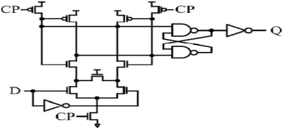
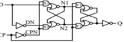
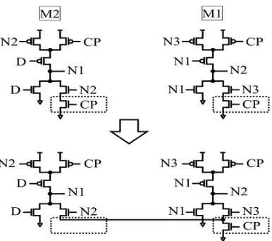
After investigating many kinds of latch circuits, we have set up an unconventionally structured FF, shown in Fig. 7. This FF consists of different types of latches in the master and the slave parts. The slave-latch is a well-known Reset-Set (RS) type, but the master-latch is an asymmetrical single data input type. The feature of this circuit is that it operates in single phase clock, and it has two sets of logically equivalent input AND logic, X1 and Y1, and X2 and Y2. Fig. 8 shows the transistor-level schematic of Fig. 7. Based on this schematic, logically equivalent transistors are merged as follows. For the PMOS side, two transistor pairs in M1 and S1 blocks in Fig. 8 can be shared as shown in Fig. 9. When either N3 or CP is Low, the shared common node becomes VDD voltage level, and N2 and N5 nodes are controlled by PMOS transistors gated N1 and N4 individually. When both N3 and CP are High, both N2 and N5 nodes are pulled down to VSS by NMOS transistors gated N3 and CP. As well as M1 and S1 blocks, two PMOS transistor pairs in M2 This article has been accepted for inclusion in a future issue of this journal. Content is final as presented, with the exception of pagination.
Fig. 7. Schematic diagram of proposed FF.
ISSN (Print) : 2320 – 3765 ISSN (Online): 2278 – 8875
I
nternational
J
ournal of
A
dvanced
R
esearch in
E
lectrical,
E
lectronics and
I
nstrumentation
E
ngineering
(An ISO 3297: 2007 Certified Organization)
Vol. 5, Issue 8, August 2016
Fig. 9. Transistor merging in PMOS side.
Fig. 10. Transistor merging in NMOS side.
ISSN (Print) : 2320 – 3765 ISSN (Online): 2278 – 8875
I
nternational
J
ournal of
A
dvanced
R
esearch in
E
lectrical,
E
lectronics and
I
nstrumentation
E
ngineering
(An ISO 3297: 2007 Certified Organization)
Vol. 5, Issue 8, August 2016
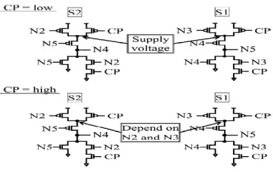
Fig. 11. Further transistor merging in PMOS side.
Fig. 12. The state of internal nodes.
Further in the PMOS side, CP-input transistors in S1 and S2, shown in Fig. 11, can be merged, because N2 and N3 are logically inverted to each other. When CP is Low, both nodes are in VDD voltage level, and either N2 or N3 is ON. When CP is High, each node is in independent voltage level as shown in Fig. 12. In consideration of this behavior, the CP input transistors are shared and connected as shown in Fig. 11. The CP-input transistor is working as a switch to connect S1 and S2. This process leads to the circuit shown in Fig. 13. This circuit consists of seven fewer transistors than the original circuit shown in Fig. 8. The number of clock-related transistors is only three. Note that there is no dynamic circuit or pre-charge circuit, thus, no extra power dissipation emerges. We call this reduction method Topological Compression (TC) method. The FF, TC Method applied, is called Topologically-Compressed Flip-flop (TCFF).
4.2 Cell Operation:
ISSN (Print) : 2320 – 3765 ISSN (Online): 2278 – 8875
I
nternational
J
ournal of
A
dvanced
R
esearch in
E
lectrical,
E
lectronics and
I
nstrumentation
E
ngineering
(An ISO 3297: 2007 Certified Organization)
Vol. 5, Issue 8, August 2016
Fig. 13. Transistor level schematic of topologically compressed flip-flop (TCFF).
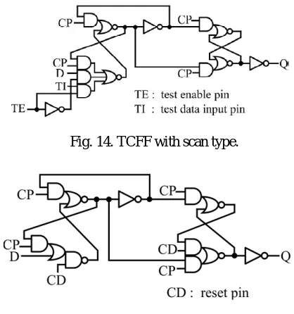
Fig. 14. TCFF with scan type.
Fig. 15. TCFF with reset type.
off, the NMOS transistor connected to CP turns on, and the slave latch becomes the data output mode. In this condition, the data in the master latch is transferred to the slave latch, and then outputted to Q. In this operation, all nodes are fully static
and full-swing. The current from the power supply does not flow into the master and the slave latch simultaneously because the master latch and the slave latch become active alternately. Therefore, timing degradation is small on cell performance even though many transistors are shared with no increase in transistor size.
4.3 Cell Variation:
LSI designs require FFs having additional functions like scan, reset, and set. The performance and cell area for these cells are also important. TCFF easily realizes these cells with less transistor-count than conventional FFs. The circuit diagrams of TCFF with scan, reset, and set are shown in Figs. 15–17. Each circuit can be designed with similar structure, and these FFs also have three transistors connected to CP so the power dissipation is nearly the same as that of TCFF.
4.4 Multi threshold vdd:
ISSN (Print) : 2320 – 3765 ISSN (Online): 2278 – 8875
I
nternational
J
ournal of
A
dvanced
R
esearch in
E
lectrical,
E
lectronics and
I
nstrumentation
E
ngineering
(An ISO 3297: 2007 Certified Organization)
Vol. 5, Issue 8, August 2016
placement of the cells. The footprint and area of low-Vt and high-Vt cells are similar. This enables timing-critical paths to be swapped by low-Vt cells easily. However, some additional fabrication steps are needed to support multiple Vt cells, which eventually lengthens the design time, increases fabrication complexity, and may reduce yield. Furthermore, improper optimization of the design may utilize more low-Vt cells and hence could end up with increased power.
V. RESULTS
Proposed flip-flop:
ISSN (Print) : 2320 – 3765 ISSN (Online): 2278 – 8875
I
nternational
J
ournal of
A
dvanced
R
esearch in
E
lectrical,
E
lectronics and
I
nstrumentation
E
ngineering
(An ISO 3297: 2007 Certified Organization)
Vol. 5, Issue 8, August 2016
ISSN (Print) : 2320 – 3765 ISSN (Online): 2278 – 8875
I
nternational
J
ournal of
A
dvanced
R
esearch in
E
lectrical,
E
lectronics and
I
nstrumentation
E
ngineering
(An ISO 3297: 2007 Certified Organization)
Vol. 5, Issue 8, August 2016
TCFF with Reset type TCFF RST:
ISSN (Print) : 2320 – 3765 ISSN (Online): 2278 – 8875
I
nternational
J
ournal of
A
dvanced
R
esearch in
E
lectrical,
E
lectronics and
I
nstrumentation
E
ngineering
(An ISO 3297: 2007 Certified Organization)
Vol. 5, Issue 8, August 2016
VI. CONCLUSION FUTURE SCOPE
This paper analyzes the existed FF topologies and suggested a compressed FF to overcome unnecessary power dissipations occurred in the FF due to their large switching activity. The proposed work may eliminate the problem of CMOS total power dissipation between logic transitions occurred in FFs. Topologically Compressed FF design improves the area utilization also this paper has realized with Layout design tools and the relevant layouts are analyzed and various physical parameters are studied at 40 nm Technology. Such designs are suggested to exhibits a competitive performance with current work.
REFERENCES
[1] H. Kawaguchi and T. Sakurai, “A reduced clock-swing flip-flop (RCSFF) for 63% power reduction,” IEEE J. SolidState Circuits, vol. 33, no. 5, pp. 807–811, May 1998.
[2] J.-C. Kim, S.-H. Lee, and H.-J. Park, “A low-power halfswing clocking scheme for flip-flop with complementary gate and source drive,” IEICE Trans. Electronics, vol. E82-C, no. 9, pp. 1777–1779, Sep. 1999.
[3] M. Matsui, H. Hara, Y. Uetani, L. Kim, T. Nagamatsu, Y. Watanabe, A. Chiba, K.Matsuda, and T. Sakurai, “A 200 MHz 13 mm 2- D DCT macrocell using sense-amplifying pipeline flip-flop scheme,” IEEE J. Solid-State Circuits, vol. 29, no. 12, pp. 1482–1490, Dec. 1994.
[4] M. Hamada, H. Hara, T. Fujita, C.-K. Teh, T. Shimazawa, N. Kawabe, T. Kitahara, Y. Kikuchi, T. Nishikawa, M. Takahashi, and Y. Oowaki, “A conditional clocking flip-flop for low power H.264/MPEG-4 audio/ visual codec LSI,” in Proc. IEEE CICC, 2005, pp. 527–530.
[5] Y. Ueda, H. Yamauchi,M.Mukuno, S. Furuichi,M. Fujisawa, F. Qiao, and H. Yang, “6.33 mW MPEG audio decoding on a multimedia processor,” in IEEE ISSCC Dig. Tech. Papers, 2006, pp. 1636–1637.