Current Differencing Transconductance
Amplifier with Improved Performance
Sunil Babu1, Rajni Prashar2
M.Tech (VLSI Design), Department of Electronics & Communication Engineering, Ajay Kumar Garg Engineering College, Ghaziabad, India
ABSTRACT: This paper presents, The Z copy current differencing transconductance amplifier (ZC-CDTA) is a new
current-mode active element that was introduced recently. ZC-CDTA is improved from the current differencing transconductance amplifier (CDTA) and has increased its universality. In the current study, a CMOS implementation of ZC-CDTA is proposed. Which has two stages of ZC-CDTA consists of a CDU (current differencing unit) and floating current source. Demands for low voltage low power integrated circuit design are growing with technology advancement. The supply voltages are ±0.9V. This ZC-CDTA provides 540.335MHz, 692.879MHz bandwidth for respective inputs and power dissipation of 0.518mW. ASM 0.18µm CMOS parameters are used for the simulations.
KEYWORDS: ZC-CDTA, CDTA, CCIII, current mode analog circuits.
I. INTRODUCTION
The Z copy current differencing transconductance amplifier (ZC-CDTA) is the modified version of the CDTA. CDTA has 2 low-impedance input terminals and 4 high-impedance output terminals. The inner structure of the ZC-CDTA is suitable to apply current-mode input signal and to obtain current-mode output signal. The possibility of low input impedance and high-output impedance provides an easy synthesis of current-mode active filters.
In the current study, a new CMOS ZC-CDTA structure is introduced. The topology proposed is composed of a current differencing unit, a dual output OTA, and a CCIII. The CCIII is used to copy the Z terminal current, where it acts as a floating current sensing active element.
There are number of advantages of current mode approach. This approach provides higher frequency range of operation, better accuracy rates, improved linearity and better accuracy.
The paper covers the implementation of design of positive feedback driven current-mode amplifiers z-copy CDBA and CDTA, and filter applications. The designed CDTA consumes extra low power and supply voltages in contrast to gate driven structures.
II. Z COPY CURRENT DIFFERENCING TRANSCONDUCTANCE AMPLIFIER (Z-CDTA)
purpose. The proposed circuit structure for the ZC-CDTA is given in Fig. 2. ZC-CDTA defining equation matrix and its basic operations formulas are given in Equation 1, 2, 3, 4, 5.
Fig. 1: Schematic view of the ZC-CDTA. Fig. 2: Proposed circuit structure of the ZC-CDTA.
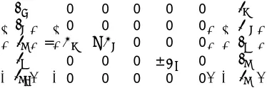
Port relation of Z-CDTA is described by following matrix.
⎝ ⎜ ⎛ ⎠ ⎟ ⎞ = ⎝ ⎜ ⎛
0 0 0 0 0
0 0 0 0 0
1 −1 0 0 0
0 0 0 ± 0
0 0 0 0 0⎠
⎟ ⎞ ⎝ ⎜ ⎛ ⎠ ⎟ ⎞
V = V = 0
I = I = I −I
I = g V
I =−g V
The defining equation of the ZC-CDTA in Figure 2 becomes Eq. (6) by considering the deviation of the voltage and the current gains from their ideal values.
⎝ ⎜ ⎛ ⎠ ⎟ ⎞ = ⎝ ⎜ ⎛
0 0 0 0 0
0 0 0 0 0
− 0 0 0
0 0 0 ± 0
0 0 0 0 0⎠
⎟ ⎞ ⎝ ⎜ ⎛ ⎠ ⎟ ⎞
And are the current gains defined by = 1-∈ and = 1-∈ . Here, ∈ and ∈ are current tracking errors, their absolute value is very close to zero.
III. CMOS IMPLEMENTATION OF ZC-CDTA
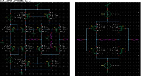
The input stage of the ZC-CDTA consists of a current differencing unit. The current differencing unit CMOS structure is given in Fig. 3.
Fig. 3: The first current differencing unit CMOS structure. Fig. 4:The floating current source CMOS structure.
The ratios of the M3 and M4transistors must be select double of the M1, M2, M5and M6 transistor ratios. Signal current is applied to the input n terminal of ZC-CDTA flows through M8 by adding M4 operating current and transferred to the M9 by current mirror. The current flowing through M3 is mirrored to M10 by the aid of M8. Signal current applied to the input p terminal of ZC-CDTA flows through M9 by adding the half of the bias current flows through M5. The half of the M4 operating current flows through M12 with the difference of p and n terminal input currents owing to M4 operating current and the n terminal current over the M9 transistor. Because of the half of M4 current over M11, the output current is the difference of the n and p terminal currents. The transistor ratios are given in Table 1.
Table 1: Transistor ratios of current differencing unit structure
The bias currents of current differencing unit are selected 100 μA. The output stage of the ZC-CDTA consists of a dual output operational transconductance amplifier. The floating current source given in Fig. 4 is used for the output stage. The structure of the floating current source consists of two inverters.
The transistors ratio of the floating current source is given in Table 2. The bias currents of the floating current
source are selected 100 μA.
Table 2: Transistors ratio of the floating current source
Transistor W(µm) L(µm) M1 - M4 1.44 0.36
IV. SIMULATION RESULTS
The simulation results for ZC-CDTA according to fig. 3 are given in figs. 5 and 6, and the parameters of the designed Z-copy CDTA are tabulated in table 3. Fig. 5 shows the IZ/IP curve of CDU (Current Differencing Unit) and
IZ/IN curve of CDU (Current Differencing Unit). Fig. 6 shows the Z terminal current with respect to P and N terminal.
The frequency responses of IZ/IP and IZ/IN are 692.879 MHz and 540.335 MHz respectively.
Fig. 5: Frequency responses of Iz/Ip and Iz/In. Fig. 6: Z terminal current with respect to P and N terminal.
Table 3: Simulation results of the ZC-CDTA
Supply voltage 0.9 V Z terminal current
dynamic range
-100 μA ≤ Iz≤ 100 μA
V. CONCLUSION
A new circuit configuration for realizing a ZC-CDTA in CMOS technology has been described. The main advantage of the designed ZC-CDTA is that it works on extra low supply voltage and power consumption. The 3dB bandwidth of IZ/IP and IZ/IN are 692.879 MHz and 540.335 MHz respectively. The proposed ZC-CDTA can be useful in application where extra low supply voltage is required. This circuit of ZC-CDTA plays important role in the low power filter design also. The performance of the proposed circuit is verified by cadence simulations using 0.18µm technology.
REFERENCES
[1] Ersin Alaybeyoglu, Arda Guney, Mustafa Altun, Hakan Kuntman 2014, “Design of positive feedback driven current-mode amplifiers Z-Copy CDBA and CDTA, and filter applications” , Springer Science Business Media New York ,Analog Integer Circ Sig Process ,Vol. 81, No. 1, pp. 109–120.
[2] Kimmo Lasanen, 2000, “A 1-V 5 μW CMOS-Op amp with bulk driven input transistors”, in Proc. IEEE MWSCAS’00, Lansing, Vol. 12, No. 1, pp. 1038–1041.
[3] Dalibor Biolek, 2003, “CDTA—building block for current-mode analog signal processing”, in Proc. ECCTD, Vol. 19, No. 3, pp. 397–40. [4] Atilla Uygur, 2005, “Multi-input multi-output cdta-based KHN filter”, Istanbul Technical University, Faculty of Electrical &Electronics
Engineering, Department of Electronics & Communications Engineering, 34469, Maslak, Istanbul, Turkey, Vol. 22, No. 1, pp. 543-552. [5] A.U. Keskin, 2006, “Current mode quadrature oscillator using current differencing transconductance amplifiers (CDTA)”, IEEE Proceeding
online no. 20050304, Vol. 45, No. 1, pp. 234-242.
[6] Ali Umit Keskin, 2006, “Current-mode KHN filters employing current differencing transconductance Amplifiers”, Int. J. Electron. Commun. (AEU), Vol. 60, No. 6, pp. 443 – 446.
[7] A. Uygur,et.al, 2006, “Low -Voltage Current Differencing Transconductance Amplifier in a Novel Allpass Configuration”, IEEE MELECON , Benalmadena (Malaga), Spain, Vol. 45, No. 1, pp. 284-292.
[8] Willy Sansen, 2007, “Analog Design Challenges in Nanometer CMOS Technologies”, IEEE Asian Solid-State Circuits Conference, Vol. 52, No. 1, pp. 4244-1360.
[9] Attila, Uygur, 2007, “Seventh-order elliptic video filter with 0.1 dB pass band ripple employing CMOS CDTAs”, Int. J. Electron. Commun. (AEU), Vol. 61, No.11, pp. 320–328.
[10] Dalibor biolek, 2008, “Active Elements for Analog Signal Processing: Classification, Review, and New Proposals”, radio engineering, Vol.17, No. 27, pp. 1341-1355.
[11]Dalibor Biolek, 2008, “High-performance current differencing transconductance amplifier and its application in precision current-mode rectification.” AEU, Int. J. Electron.Commun, Vol. 62, No. 22, pp. 92–96.
[12] Winai Jaikla, 2008, “A Simple Current-Mode Quadrature Oscillator Using Single CDTA”. radio engineering, Vol.17, No. 1, pp. 432-442. [13] Worapong Tangsrirat, 2008, “Current-Mode Multiphase Sinusoidal Oscillator Using Current Differencing Transconductance Amplifiers”,
Circuits System Signal Process, Vol. 27, No. 11, pp. 81–93.
BIOGRAPHY
Sunil Babu received the B.Tech degree in Electronics and communication engineering from Lord
Krishna College of Engineering, Ghaziabad formally Gautam Buddh Technical University, Uttar Pradesh, India in 2013. He is currently pursuing M.Tech in VLSI Design at A.K.G Engineering College, Ghaziabad (Uttar Pradesh), India. His major areas of research work include analog circuit design.
Rajni Prashar received the degree of B. Tech. in Electronics and Communication from Sant