ISSN(Online): 2320-9801
ISSN (Print) : 2320-9798
I
nternational
J
ournal of
I
nnovative
R
esearch in
C
omputer
and
C
ommunication
E
ngineering
(An ISO 3297: 2007 Certified Organization)
Vol. 4, Issue 3, March 2016
Current Mode Double Edge Triggered Flip
Flop with Enable
Remil Anita.D1, Jayasanthi.M2
PG Student, Department of ECE, Karpagam College of Engineering, Coimbatore, India1
Associate Professor, Department of ECE, Karpagam College of Engineering, Coimbatore, India2
ABSTRACT:-In this paper, a low power current mode double edge triggered flip flop with enable design is presented. A simple current mode conditional gate transmitter design is used to reduce the circuit complexity. The current mode conditional gate transmitter is combined with the current mode double edge triggered flip flop with enable(CMDETFFE) to provide one-to-many signalling which is very useful for clock distribution network. In this paper we show that when current-mode (CM) clock distribution network is used, average power can be reduced when compared with voltage-mode (VM) clocks.
KEYWORDS: Clock Distribution Network; Current-Mode; Voltage-Mode
I.INTRODUCTION
Most of the present-day systems are clock based or synchronous. These systems are built from systems, where each subsystem is a finite state machine. The subsystems changes from one state to another depending on a global clock signal which is provided by the clock distribution network. The function of clock distribution network is to synchronize millions/ billions of separate elements. The clock distribution network consumes 70% of total chip power[11].
The state updates within the subsystems are carried out on the rising or falling edge of the clock signal. A clock based system can operate correctly only if all parts of the system gets the clock at the same time, which can happen only if the delay on the clock wire is negligible. The factors influencing the clock distribution network are clock skew, jitter, power, area, slew rate. With advancement in technology, the systems tend to get bigger; as a result the delay on the clock wires cannot be ignored. Thus the problem of clock skew arises in a clock based system. Maximum difference in arrival times of clock signal to any 2 flip flops fed by the network is known as clock skew. The speed of the clock distribution can be increased by decreasing the clock skew.
The factors that determine the clock skew in a synchronous digital system are as follows:
The resistance, inductance and capacitance of the interconnection material used in the clock distribution network.
The shape of the clock distribution network.
Fabrication process variation over the area of the chip or the wafer.
Number of processing elements in the digital system and the load presented by each module to the clock distribution network.
Rise and fall times and the frequency of the clock signal.
Buffering schemes and clock buffers used.
This clock skew causes designed (unavoidable) variations, process variation, temperature gradients, IR voltage drop in power supply. The clock skew affects the timing budget and needs to be considered for maximum (setup) and minimum (hold) path timings.
Power consumption in clocks is due to clock drivers, long interconnections and large clock loads. In microprocessor 40% of total chip power is dissipated by clock. A clock network consumes silicon area and routing area. By minimizing area used, wiring capacitance and power can be reduced. To maintain signal integrity and latch performance, minimum slew rates are required.
ISSN(Online): 2320-9801
ISSN (Print) : 2320-9798
I
nternational
J
ournal of
I
nnovative
R
esearch in
C
omputer
and
C
ommunication
E
ngineering
(An ISO 3297: 2007 Certified Organization)
Vol. 4, Issue 3, March 2016
power and reliability of the current mode signalling. Since the number of sinks required is high in the clock distribution network the power consumption can be reduced by feeding current mode flip-flops[13]. The power consumption is reduced by using the symmetric flip-flop.
II.OVERVIEW OF EXISTING CM SIGNALING SCHEMES
There are two ways of current mode clock distribution. They are one to one signaling and many to one signaling schemes.
A. One-to-One Signaling:
In a CM signalling scheme, a transmitter utilizes a voltage mode input signal to transmit a current with minimal voltage swing into an interconnect, while a receiver converts current to voltage providing a full swing output voltage. In current mode signalling scheme a CMOS inverter is used as transmitter and the transimpedance amplifier is used as receiver[3]. This type signalling provides delay improvement over voltage mode scheme, but the clock skew is large in clock distribution network[4]. The clock skew can be minimized by using H-tree clock distribution as suggested in[8].The large skew problem is overcome by [6] where the dynamic over-driving technique is used but the mismatch in rise time and fall time arises. In [7] the variation-tolerant CM signalling schemes is used along with the current mode transmitter designed using bias circuitry to rectify the mismatch problem in the clock signal. In one to one current mode signaling the number of transmitter is equal to the receiver. It needs a receiver for each sink this increases the size of the circuit because which in turn increases thepower.
B. One-to-Many Signaling:
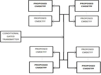
In one-to-many current mode signalling scheme, a transmitter which is designed using NAND-NOR design and the current mode pulsed flip-flop (CMPFF) is used[5]. The number of flip-flop used for receiving the clock signal is proportional to the number of sinks. The advantage of one-to-many current mode signaling is the silicon area. The silicon area decreases when the number of sink increases since it uses one transmitter and many transmitters.
The current pulsed flip flop with enable(CMPFFE)[1] uses enable signal to avoid unwanted clock signal in the area of the processor where there is no need of clock signal. But the CMPFFE is a positive edge triggered flip flop and consumes more silicon area when compared to the one-to-one current mode signalling. The CMPFFE consumes more power compared to one to one current mode signalling scheme but the static current is reduced.
III.PROPOSED WORK
A low power current mode double edge triggered flip-flop(CMDETFF) is combined with the conditional gated transmitter to do the functions of clock distribution network.The overall block diagram of the system is shown in Fig. 2.
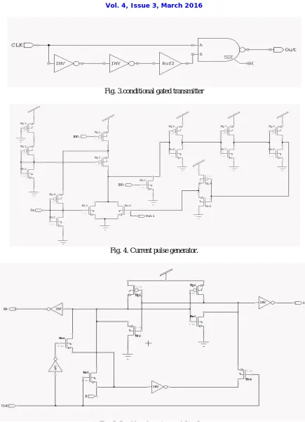
A. Conditional Gated Transmitter:
Fig. 3. Shows the circuit diagram of a conditional gated transmitter is used to produce the clock signal with constant pulse width. This is done by using a conditional AND gate. The clock signal is given as a input to AND gate and the clock signal which is delayed by using two inverters and a buffer is given as input to another pin of the AND gate. The current signal obtained from the AND gate is used as input of the proposed receiver.
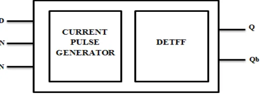
Fig. 1. Internal block diagram of Proposed CMDETFF
B. Proposed CMDTFF:
ISSN(Online): 2320-9801
ISSN (Print) : 2320-9798
I
nternational
J
ournal of
I
nnovative
R
esearch in
C
omputer
and
C
ommunication
E
ngineering
(An ISO 3297: 2007 Certified Organization)
Vol. 4, Issue 3, March 2016
Current pulse generator,
Double edge triggered flip-flop.
The internal block diagram of the proposed CMDETFF is shown in Fig. 1.
1) Current Pulse Generator:
The current pulse generator uses a global reference voltage generetor, current comparator and inverters. The global reference voltage generator is used to produce a reference current signal. The current comparator compares the current from the global reference voltage generator and the current from the transmitter to produce the current pulse. The circuit diagram of the current pulse generator is shown in Fig. 4. The current pulse is controlled by using EN signal which is given as input to the PMOS transistor Mp2 and NMOS Mn5.The current pulse generated using the current comparator is amplified using the inverters. The current pulse obtained at the pin out1 is used to triggers the double edge triggered flip-flop.
Fig. 2. Block diagram of the proposed system
2) Double Edge Triggered Flip Flop:
ISSN(Online): 2320-9801
ISSN (Print) : 2320-9798
I
nternational
J
ournal of
I
nnovative
R
esearch in
C
omputer
and
C
ommunication
E
ngineering
(An ISO 3297: 2007 Certified Organization)
Vol. 4, Issue 3, March 2016
Fig. 3.conditional gated transmitter
Fig. 4. Current pulse generator.
ISSN(Online): 2320-9801
ISSN (Print) : 2320-9798
I
nternational
J
ournal of
I
nnovative
R
esearch in
C
omputer
and
C
ommunication
E
ngineering
(An ISO 3297: 2007 Certified Organization)
Vol. 4, Issue 3, March 2016
IV.SIMULATION RESULT
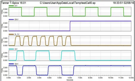
The clock signal is given as input to transmitter which transmits the signal to the receiver. The current signal from the transmitter is given as input to the receiver. The current signal taken from the transmitter is compared with the current signal generated by the global voltage generator by using current comparator. The internal current-to-voltage pulse generation is done by the current comparator and that signal is amplified by using the inverters. This current-to-voltage pulse is denoted as N_1 in the output waveform shown in Fig. 6. The EN signal is used to control the clock signal which triggers the flip-flop. Here in the simulation waveform D is the data signal given to the flip-flop and the outputs are Q and Qb.
Fig. 6. Simulation waveforms confirm the internal current-to-voltage pulse generation (N1) that triggers input data capture.
V.RESULT AND DISCUSSION
We implemented the current mode pulsed flip-flop with enable(CMPFFE) and the proposed current mode double edge triggered flip-flop(CMDETFF) in 250nm technology. The TABLE I. shows that the area of the proposed CMDETFF is reduced when compared with the CMPFFE. The power-delay- product has been increased but the static power and the average power is reduced compared with the CMPFFE.
TABLE I.RESULT COMPARISON
No. of transistors
Area (um2)
Static power (mw)
Power consumption (mw)
PDP (nj)
CMPFFE 47 31.58 25.88 2.36 103.79
Proposed CMDETFF
ISSN(Online): 2320-9801
ISSN (Print) : 2320-9798
I
nternational
J
ournal of
I
nnovative
R
esearch in
C
omputer
and
C
ommunication
E
ngineering
(An ISO 3297: 2007 Certified Organization)
Vol. 4, Issue 3, March 2016
VI.CONCLUSION
In this paper, clock distribution network have been reviewed and the pros and cons of each technique is shown. The symmetric H tree provides zero clock skew which is suitable for high speed applications. The proposed current mode DETFF clock distribution network enables 5% to 6% power reduction when compared to CMPFFE clock distribution network. The proposed CMDETFFF have reduced the area of the current mode flip-flop by 14% to 15%. The clock distribution using flip-flop is used for one to many clock distribution this discards the use of complex current mode receiver.
REFERENCES
[1] R. Islam and M. Guthaus, “Low-Power Clock Distribution Using a Current-Pulsed Clocked Flip-Flop,” in IEEE Trans. circuits and systems , vol. 62, no. 4, april 2015.
[2] F. Yuan, Cmos Current-Mode Circuits for Data Communications. New York: Springer, Apr. 2007.
[3] A. Narasimhan, S. Divekar, P. Elakkumanan, and R. Sridhar, “A low power current-mode clock distribution scheme for multi-GHz NoC based SoCs,” in Proc. 18th Int. Conf. VLSI Design, Jan. 2005, pp.130–135.
[4] N. K. Kancharapu, M. Dave, V. Masimukkula, M. S. Baghini, and D.K. Sharma, “A low-power low-skew current-mode clock distribution network in 90 nm CMOS technology,” in Proc. IEEE Comput. Soc. Annu. Symp. VLSI (ISVLSI), Jul. 2011, pp. 132–137.
[5] R. Islam and M. Guthaus, “Current-mode clock distribution,” in Proc. ISCAS, Jun. 2014, pp. 1203–1206.
[6] A. Katoch, H. Veendrick, and E. Seevinck, “High speed current-modesignaling circuits for on-chip interconnects,” in Proc. ISCAS, May2005, pp. 4138–4141.
[7] M. Dave, M. Jain, S. Baghini, and D. Sharma, “A variation tolerant current-mode signaling scheme for on-chip interconnects,” IEEE Trans.Very Large Scale Integr. (VLSI) Syst., vol. PP, no. 99, pp. 1–12, Jan. 2012.
[8] M. Nekili, Y. Savaria, G. Bois, and M. Bennani, “Logic-based H-trees for large VLSI processor arrays: A novel skew modelling and high-speed clocking method,” in Proc. 5th Int. Conf. Microelectronics,Dec. 1993, pp. 1–4.
[9] D. C. Keezer and V. K. Jain, “Clock distribution strategies for WSI: A critical survey,” in Proc. IEEE Int. Conf. Wafer Scale Integration, Jan. 1991, pp. 277–283.
[10] C. Anderson, J. Petrovick, J. Keaty, J. Warnock, G. Nussbaum, J.Tendier, C. Carter, S. Chu, J. Clabes, J. DiLullo, P. Dudley, P. Harvey,B. Krauter, J. LeBlanc, P.-F. Lu, B. McCredie, G. Plum, P. Restle,S. Runyon, M. Scheuermann, S. Schmidt, J. Wagoner, R. Weiss, S.Weitzel, and B. Zoric, “Physical design of a fourth-generation power ghz microprocessor,” in Proc. ISSCC, Feb. 2001, pp. 232–233.