NAJM, ELIE MICHEL. Design and Implementation of an Innovative Residential PV System. (Under the direction of Alex Q. Huang).
This work focuses on the design and implementation of an innovative residential PV
system. In chapter one, after an introduction related to the rapid growth of solar systems’
installations, the most commonly used state of the art solar power electronics’ configurations
are discussed, which leads to introducing the proposed DC/DC parallel configuration. The
advantages and disadvantages of each of the power electronics’ configurations are
deliberated. The scope of work in the power electronics is defined in this chapter to be
related to the panel side DC/DC converter. System integration and mechanical proposals are
also within the scope of work and are discussed in later chapters.
Operation principle of a novel low cost PV converter is proposed in chapter 2. The
proposal is based on an innovative, simplified analog implementation of a master/slave
methodology resulting in an efficient, soft-switched interleaved variable frequency flybacks,
operating in the boundary conduction mode (BCM). The scheme concept and circuit
configuration, operation principle and theoretical waveforms, design equations, and design
considerations are presented. Furthermore, design examples are also given, illustrating the
significance of the newly derived frequency equation for flybacks operating in BCM.
In chapters 3, 4, and 5, the design implementation and optimization of the novel
DC/DC converter illustrated in chapter 2 are discussed. In chapter 3, a detailed variable
frequency BCM flyback design model leading to optimizing the component selections and
circuitry related to Start-UP, drive for the main switching devices, zero-voltage-switching
(ZVS) as well as turn OFF soft switching and interleaving control are fully detailed. The
experimental results of the proposed DC/DC converter are presented in chapter 6.
In chapter 7, a novel integration method is proposed for the residential PV solar
system. The proposal presents solutions to challenges experimented in the implementation of
today’s approaches. Faster installation time, easier system grounding, and integration of the
power electronics in order to reduce the number of connectors’ and system cost are detailed.
Installers with special skills as well as special tools are not required for implementing the
proposed system integration. Photos of the experimental results related to the installation of a
© Copyright 2015 Elie Michel Najm
by
Elie Michel Najm
A dissertation submitted to the Graduate Faculty of North Carolina State University
in partial fulfillment of the requirements for the Degree of
Doctor of Philosophy
Electrical Engineering
Raleigh, North Carolina
2015
APPROVED BY:
_______________________________ ______________________________
Dr. Alex Huang Dr. Subhashish Bhattacharya
Committee Chair
________________________________ ________________________________
DEDICATION
In memory of my loved ones that I have lost during and before my PhD journey; may
they all rest in peace. I dedicate this dissertation work to my father, Michel I. Najm
(1931-2012), my mother-in-law Saada G. Maalouf (1945-2013), and to my late uncles and
grandparents. I will never forget that in the midst of a war devastated country, my
grandfather, Khalil A. Jabbour, drove me to the Beirut International Airport in August 21,
1978, under the wrath of fighting, waiting for hours until he made sure that my plane to the
BIOGRAPHY
Elie Najm operated as a technical leader at IBM Power Electronics System for the Networking Hardware Division from 1982 to 1996. He has held senior management positions in the construction industry, in the U.S. and overseas, from 1997 to 2010. He was admitted as a PhD student in 2010 at North Carolina State University (NCSU) and has performed as a research assistant at NCSU FREEDM Systems Center.
Elie’s research areas are solar energy, power electronics, analog electronic circuits and systems, power system architecture, and system integration. At FREEDM, he has led the System Integration and Demonstration as well as the Electrical System Improvements’ teams for the “Cost Effective, Residential Plug and Play Photovoltaic System,” sponsored by the U.S. Department of Energy (DOE) SunShot Initiative. He has designed and developed a low cost solar converter in line with the SunShot cost target of $0.12 per watt. He has also directed the system engineering for the NSF supported FREEDM Systems Center’s Green Energy Hub project (GEH). Furthermore, he has led activities such as the performance evaluation and test box designs for a Solar powered 40kW UPS developed by Eaton Corp. He has published several papers as a result of his research.
While working for IBM, Elie has received 6 patents and 21 technical disclosures as well as multiple awards to include the “IBM Invention Achievement Award” and the “IBM Outstanding Innovation Award.” He was featured numerous times in the IBM Vital Signs publication.
ACKNOWLEDGMENTS
I would like to thank my advisor and mentor, Professor Alex Q. Huang for his
continuous guidance and support throughout the process. I am grateful for his efforts in
bringing out the best in me in this sound North Carolina State University’s PhD program.
The dedication that Dr. Huang offers to all his students is beyond all expectations. It has been
a great experience serving under the leadership of a scholar such as Professor Huang.
I would also like to extend my appreciation to my committee members, Dr. Mesut
Baran, Dr. Subhashish Bhattacharya, and Dr. John Mackenzie for their assistance, direction,
and support. Under Dr. Baran’s leadership, I was able to complete and receive the Graduate
Certificate in Renewable Electric Energy Systems in 2014.
My gratefulness also goes to all members in the FREEDM Systems Center. The
support that I have received from Drs. Iqbal Hussein (FREEDM director), Wensong Yu,
Douglas Hopkins, David Lubkeman, Rogelio Sullivan, Ewan Pritchard, and all the other
FREEDM faculty and staff, has been instrumental. The lab manager, Hulgize Kassa, and his
assistant Gregory Norris, have persistently upheld a positive and safe lab environment. The
continuous assistance from Colleen Reid and Karen Autry has been essential in my long PhD
journey.
I would like to express my indebtedness to my long time good friend, Charles Weant.
Charles played a crucial role in the DOE solar PnP project’s prototyping and system
integration. Furthermore, post doctorates, such as Dr. Ruiyang Yu, aided me on several
occasions, while so many great students, such as Mohammad Ali Rezaei, Md Tanvir Arafat
Khan, Qingyun Huang, Dr. Fei Wang, and several others that I have worked with, have
I have been blessed to have the love and support of my family. I am grateful to my
caring and beautiful wife, Rita; to my 6 children: Yvone, Michael (Micho), Joseph (whom I
have been constantly praying for), Rita (Rattout), Christian (#7), and Julian (the angel of the
family); to my daughter-in-law, Eya, and to my grandchildren: Elie (Leo) and Aiden
(Addouni). Yvone, who has also graduated from NCSU, did carry us financially throughout
my NCSU journey. It brings tears to my eyes just to think about the sacrifices that she has
made; I am so proud of her.
I am also blessed for my heavenly gift: My mother. She has always been there for me,
my brothers, and the big family. The Lord has indeed been so kind to me with such a loving
family, which is much more than I deserve.
Table of Contents
LIST OF TABLES ... ix
LIST OF FIGURES ... xi
Chapter 1: Introduction and System Architecture……… 1
1-1 Introduction ... 1
1-2 U.S. Residential Solar Energy Installations ... 4
1-3 U.S. Residential Solar Energy Installations Cost Trend ... 5
1-4 Solar System State of the Art Configurations – Power Electronics ... 7
1-4-1 String or Center Inverter Configuration ... 7
1-4-2 AC Parallel (Micro-Inverter) Configuration ... 8
1-4-3 AC Series Configuration ... 9
1-4-4 DC Series Configuration ... 11
1-5 Proposed System Configuration – Power Electronics ... 12
1-5-1 Desirable Residential PV System ... 12
1-5-2 Proposed Power Electronics’ Configuration – Integrated DC Parallel ... 14
1-6 Conclusion ... 17
Chapter 2: Operation Principle of a Novel Low Cost PV Converter Based on Analog Interleaving Method………18
2-1 Overview ... 18
2-2 Prior Arts ... 19
2-3 Configuration and Operation Principle of the Proposed Circuit ... 21
2-3-1 Scheme Concept and Circuit Configuration ... 21
2-3-2 Operation Principle and Theoretical Waveforms ... 24
2-3-3 Design Equations... 28
2-3-4 Operating Frequency vs. Q1’s Drain Node Capacitance ... 36
2-3-5 Operating Frequency vs. Input Power ... 37
2-4 Design Considerations of the Proposed Circuit ... 40
2-5 Conclusion ... 41
Chapter 3: Design Model for the Novel Low Cost PV Converter Based on Analog Interleaving Method………43
3-1 Overview ... 43
3-2 Variable Frequency BCM Flyback Design Model Digest ... 44
3-3 Variable Frequency BCM Transformer Design ... 50
3-3-1 Undesired Transformer Performance Design Summary ... 51
3-3-2 BCM Flyback Transformer Ferrite Material Selection ... 52
3-3-3 Winding Transformers for Minimum Leakage Inductance ... 57
3-5 Design for 250W PV Panel ... 57
3-5-1 DC-DC Converter Electrical Specifications ... 58
3-5-2 Design Implementation ... 59
3-6 Conclusion ... 63
Chapter 4: Design Optimization for the Novel Low Cost PV Converter Based on Analog Interleaving Method………65
4-1 Overview ... 65
4-2 Design Optimization for the BCM Flyback Power MOSFETs ... 65
4-2-1 MOSFET Voltage Ratings’ Selection ... 66
4-2-2 Optimization for the MOSFET’s Conduction Losses ... 69
4-2-3 MOSFET Gate Charge Requirements ... 75
4-2-4 Metal Oxide versus Gallium Nitride ... 76
4-3 Magnetic Design Optimization ... 78
4-3-1 Ferrite Core Losses ... 79
4-3-2 Duty Cycle Optimization for Minimum Core Losses ... 83
4-4 Minimum Operating Frequency Selection Optimization ... 84
4-5 Phase Shading Optimization ... 87
4-6 Silicon versus SiC for the Output Rectifier ... 88
4-7 Conclusion ... 91
Chapter 5: Circuit Design Innovations Implemented In the Novel Low Cost PV Converter Based on Analog Interleaving Method………..92
5-1 Overview ... 92
5-2 Novel Startup Circuit ... 93
5-3 Main Switching Devices Novel Turn ON Circuit ... 95
5-4 Main Switching Devices Novel Turn OFF Circuits ... 97
5-5 Novel Control Circuit ... 99
5-6 Short Circuit Protection ... 101
5-7 Analog versus Digital Circuits ... 102
Chapter 6: Experimental Results of the Novel Low Cost PV Converter Based on Analog
Interleaving Method………..106
6-1 Overview ... 106
6-2 250W Prototype ... 106
6-3 250W Prototype Bill of Material ... 108
6-4 Key Waveforms ... 110
6-5 Efficiency ... 117
6-6 Conclusion ... 118
Chapter 7: Innovative Plug and Play Residential PV System Design and Implementation119 7-1 Overview ... 119
7-2 Proposed Innovative Mechanical Integration of Residential Roof Mount Racking System Digest ... 119
7-3 Proposed Innovative PnP Integration System Configuration ... 122
7-4 Proposed Innovative PnP Integration System Installation Procedure ... 124
7-4-1 2kW Racking System ... 125
7-4-2 1kW Racking System ... 132
7-5 Innovative PnP System Experimental Results ... 146
7-6 Comparison with Current Integration and Installation Methods ... 148
7-7 Conclusion ... 150
Chapter 8: Conclusion………152
8-1 Conclusion ... 152
8-2 Future Work ... 154
LIST OF TABLES
Table 1.1: Renewable Energy Indicators 2013 as provided by REN21 ... 2 Table 1.2: Top five countries’ annual investment/net capacity additions/production in
2013 ... 3 Table 1.3: Top five countries’ total capacity of generation as of the end of 2013 ... 3 Table 1.4: Residential PnP solar system cost table as developed in 2013 by NCSU
FREEDM Systems Center in response to the DOE SunShot initiative grant ... 13
Table 3.1: Ferrite material approximate core losses using the RM14 core set operating at B = 2000 mT and loss curves as provided by EPCOS ... 55 Table 3.2: Ferrite material approximate core losses using the RM14 core set operating at
B = 1000 mT while doubling the frequencies shown Table 3.1, and loss curves as provided by EPCOS ... 55 Table 3.3: Electrical specifications for the DC/DC converter in a DC parallel approach . 58 Table 3.4: Transformer losses breakdown ... 63 Table 3.5: Transformer bobbin buildup ... 63
Table 4.1: Unit cost and device parameters of few selected 200V voltage rating metal oxide N-channel MOSFETs, where the data are extracted from Digi-Key Electronics’ website ... 66 Table 4.2: Unit cost and device parameters’ comparison among various voltage rating
MOSFETs that are suitable for the proposed converter, where the data are extracted from Digi-Key Electronics’ website ... 67 Table 4.3: Effect on the duty cycle and the RMS drain current as VREFL varies from 10V
to 80V while holding VIN at 30V, PIN,max for each of the interleaved flybacks at 125V, and CS1 at 10nF ... 70 Table 4.4: MOSFET conduction loss (PCOND,max,M) calculation based on (117), using the
rDS,ON values in the data range provided in Table 4.1 while varying the output
reflected voltage (VREFL) from 10V to 80V. The input voltage (VIN) is held at 30V, the input power (PIN,max) for each of the interleaved flybacks at 125W, and CS1 at 10nF .. 72 Table 4.5: MOSFET conduction loss (PCOND,max,M) is based on (121), using the rDS,ON values
Table 4.7: 100V GaN & RM12 core set versus 100V silicon & RM14 core set comparison
... 78
Table 4.8: Comparison between the Silicon Carbide (SiC) and the ultra-fast recovery glass passivated rectifiers ... 90
Table 5.1: Cost of using a digital microcontroller ... 103
Table 5.2: Cost of using the employed innovative analog circuits ... 104
Table 6.1: Prototype BOM cost summary ... 108
Table 6.2: Prototype BOM ... 109
Table 7.1: Bill of Material of the proposed integrated PnP system ... 124
Table 7.2: Residential solar installation time comparison ... 149
LIST OF FIGURES
Figure 1.1: Global renewable electricity production by region, historical and projected ... 1
Figure 1.2: U.S. PV installations, Q2 2010–Q2 2014 ... 4
Figure 1.3: Modeled residential turnkey system pricing with cost breakdown, Q1 2014– Q2 2014 ... 5
Figure 1.4: Median reported installed prices of residential and commercial PV systems over time ... 6
Figure 1.5: Reported, bottom-up, and analyst-projected average U.S. PV system prices over time ... 6
Figure 1.6: String (central) inverter configuration ... 7
Figure 1.7: AC parallel (micro-inverter) configuration ... 8
Figure 1.8: AC series configuration ... 10
Figure 1.9: DC series configuration ... 11
Figure 1.10: Proposed integrated DC parallel configuration ... 15
Figure 2.1: Proposed scheme concept ... 22
Figure 2.2: Novel Low Cost PV Converter (or Micro-Inverters) Based on Analog Interleaving Method ... 23
Figure 2.3: Detailed operation of the proposed scheme ... 27
Figure 2.4: BCM flyback basic configuration ... 28
Figure 2.5: BCM flyback basic configuration during tON ... 28
Figure 2.5(a): BCM flyback basic configuration during tON ... 29
Figure 2.5(b): BCM flyback basic configuration during tOFF1 ... 30
Figure 2.5(c): BCM flyback basic configuration during tOFF2 ... 31
Figure 2.6: BCM flyback primary and secondary current waveforms ... 32
Figure 2.7: BCM flyback primary winding voltage waveform ... 33
Figure 2.8: BCM flyback operating frequency versus Q1’s drain node capacitance ... 37
Figure 2.9: BCM flyback operating frequency versus input power (PIN). The blue line illustrates the frequency variations while ignoring CS1. The burgunday line shows the frequency while taking CS1 into account. The green line illustrates the experimental results, which agrees with the results provided by (51) ... 40
Figure 3.2: Ferrite material loss curves as provided by EPCOS ... 56 Figure 3.3: RM14 core set specifications as provided by the EPCOS catalog ... 59 Figure 3.4: One of the suitable bobbin specifications for the RM14 core set, as provided
by the EPCOS catalog ... 60
Figure 4.1: BCM flyback main switching MOSFET drain to source voltage (VDS)
waveform, where the maximum voltage seen is the sum of the input, reflected, and the overshoot voltages. ... 69 Figure 4.2: BCM flyback main switching MOSFET drain to source RMS current as VREFL
varies from 10V to 80V while holding VIN at 30V, PIN,max for each of the interleaved flybacks at 125W, and CS1 at 10nF ... 71 Figure 4.3: BCM flyback duty cycle (δ) increases as VREFL increases from 10V to 80V
while holding VIN at 30V, PIN,max for each of the interleaved flybacks at 125W, and CS1 at 10nF ... 71 Figure 4.4: MOSFET conduction loss (PCOND,max,M) calculation based on (117), using the
rDS,ON values in the data range provided in Table 4.1 while varying the output reflected voltage (VREFL) from 10V to 80V. The input voltage (VIN) is held at 30V, the input power (PIN,max) for each of the interleaved flybacks at 125W, and CS1 at 10nF ... 73 Figure 4.5: MOSFET conduction loss (PCOND,max,M) calculations based on (117), using the
devices illustrated in Table 4.6, while varying the output reflected voltage (VREFL) from 10V to 30V for the 80V device, 10V to 40V for the 100V device, and from 10V to 80V for the 150V device. The input voltage (VIN) is heldat 30V, the input power
(PIN,max) for each of the interleaved flybacks at 125W, and CS1 at 10nF ... 75 Figure 4.6: Flyback converter with discontinuous current path [27]. This is also
applicable to BCM flyback where the deadtime is equal to tOFF2 given in equation (24) ... 82 Figure 4.7: Core losses versus operating frequency, N97 and N95 comparison, using the
EPCOS “Ferrite Magnetic Design Tool ver.5.2.1.” for the core and material selection for the DCM Flyback converter [28], which is also applicable for a BCM flyback with a deadtime equal to tOFF2, as given in equation (24). Assuming that VREFL = VIN = 30V,
Lm1 = 14 μH, CS1 = 15 nF, f = 50 kHz, B = 200 mT, and T = 80°C ... 82 Figure 4.8: Ratio of the actual core loss to its sinusoidal signal value (rx-1) versus the duty
cycle, N97 and N95 comparison using the EPCOS “Ferrite Magnetic Design Tool ver.5.2.1.” for the core and material selection for the DCM Flyback converter [27], which is also applicable for a BCM flyback with a deadtime equal to tOFF2, as given in equation (25). Assuming that VREFL = VIN = 30V, Lm1 = 14 μH, CS1 = 15 nF, f = 50 kHz,
Figure 4.9: Experimental results showing the drain to source voltage and current
waveforms crossover of a power MOSFET used in the Novel Low Cost PV Converter Based on Analog Interleaving Method at turn OFF. The time scale is at 100nS/div., the voltage and current scales are 20V/div. and 10A/div. simultaneously. The data was taken at full input power of 250W, where each of the interleaved flyback sees 125W.
The input voltage VIN = 30V ... 85
Figure 4.10: Turn OFF losses of Q1 and Q1 + Q2 versus the operating frequency in an interleaved BCM flyback ... 86
Figure 4.11: Waveforms for T1’s primary and secondary voltage as well as D1’s current . 89 Figure 4.12: Experimental results illustrating the master flyback’s current waveforms of the output rectifier (D1 in green) and the drain to source of MOSFET (Q1 in pink) along with Q1’s drain to source voltage (in blue) ... 90
Figure 5.1: Novel startup circuit ... 94
Figure 5.2: Novel startup circuit sequence ... 95
Figure 5.3: Novel turn ON circuit ... 96
Figure 5.4: Novel turn ON circuit waveforms ... 97
Figure 5.5: Novel turn OFF circuit ... 98
Figure 5.6: Novel turn OFF circuit waveforms ... 98
Figure 5.7: Novel control circuit ... 100
Figure 5.8: Digital microcontroller’s manufacturer recommended minimum connection, where L1 is specified to have an impedance of less than 1Ω ... 103
Figure 5.9: Digital microcontroller’s manufacturer exemplified application example illustrating the need to add FET driver modules ... 104
Figure 6.1: Scheme PCB top layer ... 107
Figure 6.2: Scheme PCB bottom layer ... 107
Figure 6.3: Scheme 250W prototype ... 107
Figure 6.4: Gate to source and drain to source waveforms of the master and slave main switching MOSFETs at full load ... 111
Figure 6.5: Master and slave main switching MOSFETs’ drain and output rectifier current waveforms at full load ... 112
Figure 6.7: Slave’s output rectifier current; main switching MOSFETs’ drain current and
gate & drain voltage waveforms at full load ... 113
Figure 6.8: Scheme’s updated 250W prototype(2” by 7.7”) ... 113
Figure 6.9: The peak drain to source voltage of the master flyback’s MOSFET is shown to be 65V at full load. The turn OFF drain to source current (Q1,ids) and voltage (Q1,vds) crossover is measured at 100ns per division ... 114
Figure 6.10: The peak drain to source voltage of the slave flyback’s MOSFET is shown to be 67V at full load. The turn OFF drain to source current (Q2,ids) and voltage (Q2,vds) crossover is measured at 100ns per division ... 114
Figure 6.11: Drain to source current (Q1,ids) and voltage (Q1,vds) crossover is measured at 1µs per division. The figure illustrates ZVS turn ON at full load ... 115
Figure 6.12: Drain to source current (Q2,ids) and voltage (Q2,vds) crossover is measured at 1µs per division. The figure illustrates ZVS turn ON at full load ... 115
Figure 6.13: Adopted analog control method response to PV irradiance increase. The input current change is almost immediately followed by that of the output ... 116
Figure 6.14: Adopted analog control method response to PV irradiance decrease. The input current change is almost immediately followed by that of the output ... 116
Figure 6.15: Efficiency performance of prototype presented in Fig. 6.3 ... 117
Figure 6.16: Efficiency performance of the updated prototype presented in Fig. 6.8 ... 117
Figure 7.1: Residential roof mount racking PV solar racking system provided by IRONRIDGE ... 120
Figure 7.2: The Zilla Double Stud XL Flashing attaches to sheathing or structural members of the roof, not required to be fastened to the roof rafters ... 120
Figure 7.3: Proposed use of spacers to form the racks, cable management, and to integrate the power electronics ... 121
Figure 7.4: Illustration of the proposed PnP system configuration of the integrated DC/DC parallel (suitable for any power electronics’ topology architecture) ... 123
Figure 7.5: Installation procedure step 1 ... 125
Figure 7.6: Installation procedure step 2 ... 126
Figure 7.7: Installation procedure step 3 ... 127
Figure 7.8: Installation procedure step 5 ... 127
Figure 7.9: Installation procedure step 6 ... 128
Figure 7.10: Installation procedure step 7 ... 129
Figure 7.12: Installation procedure step 9 ... 130
Figure 7.13: Installation procedure step 10 ... 130
Figure 7.14: Installation procedure step 11 ... 131
Figure 7.15: Installation procedure step 12 ... 131
Figure 7.16: Installation procedure step 13 ... 132
Figure 7.17: Installation procedure step 14 ... 133
Figure 7.18: Installation procedure step 15 ... 134
Figure 7.19: Installation procedure step 16 ... 134
Figure 7.20: Installation procedure step 17 ... 135
Figure 7.21: Installation procedure step 18 ... 135
Figure 7.22: Installation procedure step 20 ... 136
Figure 7.23: Installation procedure step 21 ... 137
Figure 7.24: Installation procedure step 22 ... 137
Figure 7.25: Installation procedure step 23 ... 138
Figure 7.26: Installation procedure step 24 ... 138
Figure 7.27: Installation procedure step 25 ... 139
Figure 7.28: Installation procedure step 26 ... 139
Figure 7.29: Installation procedure step 28 ... 140
Figure 7.30: Installation procedure step 29 ... 140
Figure 7.31: Installation procedure step 30 ... 141
Figure 7.32: Installation procedure step 31 ... 141
Figure 7.33: Installation procedure step 32 ... 142
Figure 7.34: Installation procedure step 33 ... 142
Figure 7.35: Installation procedure step 34 ... 143
Figure 7.36: Installation procedure step 35 ... 143
Figure 7.37: Installation procedure step 36 ... 144
Figure 7.38: Installation procedure step 38 ... 145
Figure 7.39: 3 kW residential PnP solar system installation designed according to the proposed approach ... 145
Figure 7.40: Proposed 3-pin panel connector to replace the MC4 panel connectors ... 146
Figure 7.42: Installed integrated racking system performed according to the proposed method ... 147 Figure 7.43: Installed integrated 3kW system performed according to the proposed
Chapter 1: Introduction and System Architecture
1-1
Introduction
In its 2014 medium-term renewable energy market report [1], the International
Energy Agency (IEA) has published that the global renewable electricity generation has
increased by an estimated 240 terawatt hours (TWh) in 2013, which represent a growth of
5% from the prior year. Furthermore, the report also indicated that with such a growth, the
renewable electricity generation has reached nearly 5070 TWh, which accounted for
approximately 22% of total power generation. Moreover, it has also indicated that the
renewable capacity rise due to the deployment of hydropower and solar PV was faster than
expected. Fig. 1.1 illustrates the historical and projected global renewable electricity
production by region [1].
On the other hand, the Renewable Energy Policy Network for the 21st Century
(REN21), in their Renewables 2014 Global Status Report [2], stated that “Around the world,
major industrial and commercial customers are turning to renewables to reduce their energy
costs while increasing the reliability of their energy supply.” Furthermore, the REN21 report
agreed with the REA above referenced report regarding the rapid growth of Solar PV
installations. It stated that “Solar PV has continued to expand at a rapid rate, with growth in
global capacity averaging almost 55% annually over the past five years.” Table 1.1 illustrates
the years 2012 and 2013 figures of the global utilization of renewable energy [2].
Moreover, [2] indicated that countries like United States, China, Germany, Canada,
and Brazil, have maintained their status as the topmost countries that have deployed
renewable power capacity. As of the end of 2013, the list of the top five countries’
investment in renewable power and fuels is illustrated in Table 1.2, while the total capacity
or generation is illustrated in Table 1.3.
Table 1.2: Top five countries’ annual investment/net capacity additions/production in 2013. [2]
1-2 U.S. Residential Solar Energy Installations
Based on its 2014 second quarter Solar Market Insight Report [3], the Solar Energy
Industries Association (SEIA) has claimed that as much as 1,133 MWdc of solar PV was
installed in the United States in the second quarter of 2014. The report also claimed that such
a figure represents an increase of 21% in solar installations over the second quarter of 2013,
which is the 4th largest quarter in the history of the market. Furthermore, the report also
stated that “PV installations will reach 6.5 GWdc in 2014, up 36% over 2013 and more than
three times the market size of just three years ago.” Moreover, the report also claimed that
the U.S. residential solar market has seen steady growth, up 45% over the second quarter of
2013, where over 100 MWdc were installed in the second quarter of 2014, without any state
incentive. Fig. 1.2 illustrates the U.S. PV installations’ trend from the second quarter of 2010
up to the second quarter of 2014 [3].
1-3 U.S. Residential Solar Energy Installations Cost Trend
A major factor behind the steady growth of solar installations in the U.S. residential
market is related to cost. In addition to the government incentives, the residential solar
system cost has decreased a great deal in the past several years. Based on [3], “the cost of
solar has come down enough that more customers can afford to pay the cash.” Fig. 1.3
illustrates the related cost reduction in one quarter only (first quarter of 2014 to second
quarter of 2014) of the residential turnkey solar system pricing.
The history of reducing the cost of residential solar installations is also provided by
the National Renewable Energy Laboratory (NREL) in its September 2014 report [4]. NREL
claimed that the median pricing for residential and small commercial (≤ 10 kW) PV system
installations completed in 2013, “based in part on data reported to PV incentive programs,”
was $4.69/W. Furthermore, the report also indicated that the “reported system prices of
residential and commercial PV systems declined 6%–7% per year, on average, from 1998–
2013, and by 12%–15% from 2012–2013, depending on system size.” Fig. 1.4 illustrates the
cost trend as provided by the said report.
Moreover, [4] also provided a curve related to the projected average of the U.S. PV
system prices over time. The said curve is illustrated in Fig. 1.5, where the brown line
illustrates the reported median residential system price. In addition, the reported system price
shown in Fig. 1.5 assumes that the residential market median price is for systems that are less
than or equal to 10 kW. The shown modeled residential system price exemplifies a 5 kW as
an approximate residential system.
Figure 1.4: Median reported installed prices of residential and commercial PV systems over time. [4]
1-4 Solar System State of the Art Configurations – Power Electronics
Several solar system architectures are currently utilized in residential applications (as
well as commercial applications). The following is a brief description as well as highlight
summary of the advantages and disadvantages of each.
1-4-1 String or Center Inverter Configuration
Fig. 1.6 exemplifies the string (central) inverter approach, which does not require
power converter modules per panel. Instead, a central-inverter box to include communication
and control per string is installed. In such configuration, the solar panels are connected in
series to form an array, with a typical output voltage rating of 300 to 600VDC. The array
output is connected to a single inverter, with an AC output that is typically tied to the grid.
All communication circuitry are embedded in the central inverter. The following is a list of
some of the main advantages and disadvantages of the string inverter configuration:
Advantages:
- Well established single stage configuration.
- Built-in isolation for solar panels.
- Lowest system component cost approach.
Disadvantages:
- Lack of distributed maximum power point tracking (MPPT), which results into lower
system efficiency.
- The maximum output performance is limited by the worst performing solar panel
(partial shading, manufacturing defect, dust, etc.).
- Presence of high DC voltage (sum of string of PV panel voltages) that necessitates
additional protection steps, as required by national electric code (NEC) regulations.
1-4-2 AC Parallel (Micro-Inverter) Configuration
The AC parallel (micro-inverter) configuration, illustrated in Fig. 1.7, consists of
several parallel PV modules that each includes a DC/AC inverter. Such parallel DC/AC
inverters are connected to form an AC grid connected solar energy system. The maximum
power point (MPP) operation of each panel can be guaranteed with this configuration and
modular design is easily achievable. The market available DC/AC inverter products, such as
the one provided by Enphase Energy, embed communication circuitry in each of the
micro-inverters, which communicates with its system gateway.
Advantages:
- Isolation is easily achieved in the DC/AC parallel configuration
- The DC/AC inverter can be PV panel integrated (typically at the back), where no
centralized inverter is needed, which could lead to easier installation.
- Independent MPPT control could be implemented to maximize the solar energy
output for each PV panel.
- Single stage conversion approach (DC/AC inverter between the panel and the grid),
which is a potentially higher efficiency system.
- Each DC/AC inverter has its own control, which makes it simple to add and remove
panels to the system.
- Absence of high system DC voltage, which eliminates the need to adhere to related
stringent NEC requirements.
Disadvantages:
- Higher system cost due to redundant circuitry, such as communication, control, etc.
- More connectors are used in the system, which increases cost and installation time.
1-4-3 AC Series Configuration
One interesting approach, which is being developed at the North Carolina State
University’s FREEDM Center, is the AC series configuration, which is illustrated in Fig. 1.8.
The AC series configuration consists of several series PV modules that each includes a
DC/AC inverter. The MPP operation of each panel can also be guaranteed with this
Advantages:
- The DC/AC inverter can be integrated at the back of the PV panel and no centralized
inverter is needed, which would lead to easier installation.
- Independent MPPT control can be employed to maximize the solar energy output for
each PV panel.
- Single stage DC/AC inverter can eliminate one stage of power conversion, hence
potentially increase the efficiency of the system.
- Series connected modules allow transformerless connection to the grid, which
contributes to lowering the cost and an approximate reduction of 1% in electrical
losses.
Disadvantages:
- The system is not isolated if the transformerless approach is adopted in the DC/AC
inverters.
- The system reliability is reduced due to the series connection configuration.
- The control circuitry is technically more challenging in the AC series approach.
- Potentially low system cost (but higher than the string inverter approach) due to
redundant circuitry, such as communication, control, etc.
1-4-4 DC Series Configuration
The DC Series configuration is shown in Fig. 1.9. It consists of several series PV
modules where each includes a DC/DC converter (optimizer). Unlike the DC Parallel
configuration illustrated later in this chapter, the DC Series output voltage is relatively low,
which allows for the use of low voltage switching devices. This presents advantages in cost
and efficiency. Furthermore, the efficiency is further optimized since each of the DC/DC
converters includes its own MPPT function. However, the efficiency is reduced by 1 to 2%
due to the need of the 2-stage system, as this configuration requires a DC/AC inverter placed
between the panel string and the grid. The market available DC/DC converter products, such
as the one provided by Tigo Energy, Incorporation, embed communication circuitry in each
of the converters, which communicates with its system gateway and energy management
unit.
Advantages:
- Independent MPPT control can be implemented for each PV panel.
- DC/DC converter panel mounted modules are very efficient due to the use of
relatively low voltage switching devices.
Disadvantages:
- Power sharing in the series DC/DC converters represents design challenges.
- Uses two-stage architecture. Therefore, some of the efficiency gain at the DC/DC
converter module level is lost at the second stage.
- The system reliability is reduced due to the series connection configuration.
- Higher system cost (but lower than the DC/AC parallel approach) due to redundant
circuitry, such as communication, control, etc.
- More connectors are used in the system, which increase installation time.
1-5 Proposed System Configuration – Power Electronics
1-5-1 Desirable Residential PV System
From section 1-3 we see that the residential solar system cost reduction is the main
driver behind its continuous growth. Furthermore, as of the past few years, the U.S.
Department of Energy (DOE) has been funding activities associated with cost reducing the
residential solar systems. An example of the related DOE activities is the launch of the
SunShot initiative, which includes the residential Plug and Play (PnP) solar system. In 2013,
The FREEDM Center at North Carolina State University (NCSU) was awarded a segment of
the related grant. In response to the said initiative’s cost objectives of a total of $1.50 per
target cost breakdown for the system that would make it possible for the $1.50/W target to be
realized. Such cost breakdown is illustrated in Table 1.4.
Therefore, an innovative low cost system configuration, along with its innovative low
cost components, is anticipated. On the other hand, prior to proposing a new solar system
configuration, having in mind that the residential market is the main focus of this research, it
is desired to introduce a list of commonsense requirements that would lead to an optimum
residential solar system. While there is no such thing as a perfect structure, the desired
system would need to meet the following sequentially prioritized list:
1. Safe
2. Low cost
3. Reliable
4. Flexible
Table 1.4: Residential PnP solar system cost table as developed in 2013 by NCSU FREEDM Systems Center in response to the DOE SunShot initiative grant.
$0.50 $0.12
Installation $0.15
Racks and Accessories $0.11
Permitting $ -
Inspection $ -
Component Interconnection $0.05
Gird Connection $0.03
Controls and Interfaces $0.07
Overhead (9%) $0.09
Profit (25%) $0.28
Taxes (7%) $0.10
$1.50 TOTAL
System Details End of Project Cost Target
5. Scalable
6. Simple to implement and Easy to install
A detailed discussion in relation to the above points in a desired residential PnP PV
system will be presented in a later chapter. While an innovative low cost mechanical system
is a key element of the PnP system, the focus of this chapter is to introduce the proposed
innovative low cost power electronics’ system topology and architecture. A low cost
mechanical proposal, suitable for the residential PnP PV system is introduced in a later
chapter.
1-5-2 Proposed Power Electronics’ Configuration – Integrated DC Parallel
From section 1.4 of this chapter, each of the state of the art power electronics’
configurations presents advantages and disadvantages. As an introduction to the succeeding
chapters, in this section, the DC parallel configuration is introduced. Such an approach,
illustrated in Fig. 1.10, consists of 4-in-1 or 6-in-1 or 8-in-1 (as suitable for the application)
integrated parallel DC/DC converters, where each converter is associated with one PV
module. Hence, the MPP operation of each PV panel is optimized. The outputs of the said
parallel converters are connected to a proportional second stage DC/AC inverter, which is
integrated with the related DC/DC converters in one mechanical enclosure.
While the inverter’s function is to transfer the solar energy to the grid, it is proposed
to also be designed where its DC input (VDC,IN) be regulated to a voltage level slightly higher
than the peak of the maximum AC grid voltage that it is connected to, such that
, , ,max.
DC IN AC peak
V V In order to simplify the design of the system, elimination of costly
proposal:
1) Provide isolation (where required) in the DC/DC converters, where it is no longer
needed in the inverter.
2) All outside communications (from the output of the inverter to the rest of the world)
to be incorporated in the inverter and only limit the DC/DC converter’s embedded
communications, or functions, to:
a. Enabling start-up and activating shutdown through sensing for the presence of
the grid voltage by sensing the presence of the inverter’s DC input voltage.
b. Ability to react to instructions from the inverter, as directed by the utility
companies, to perform power curtailment and other as such features.
c. Since the proposed system is a DC parallel system, sensing the proper
operation of each PV panel and/or its related DC/DC converter could easily be
done at the inverter’s level. Hence, no special communication features need to
be provided by the DC/DC converter.
3) Each DC/DC converter to have its own overcurrent and input/output overvoltage
protection.
Advantages:
- The parallel configuration guarantees the high reliability of the PV system.
- The cost of the said integrated configuration is potentially low due to:
Reducing the number of connectors needed for the system
Reducing the number of power electronics’ mechanical enclosures
Potentially reducing the number of components related to the power electronics’
circuitry and lowering the cost of the employed printed circuit board (PCB)
- Independent MPPT control can be implemented for each PV panel.
- System isolation from the grid is realizable.
- High DC voltage is not exposed. Hence, eliminating the need for meeting related
stringent NEC requirements.
- Each DC/DC converter has its own control and plug-and-play can be realized easier.
Disadvantages:
- In the absence of circuit innovations, higher system cost is a concern since the
DC/DC converter is needed for each PV panel.
- The efficiency of the system suffers due to the two stage architecture.
The residential PnP PV system illustrated in the remaining chapters, proposes novel
solutions to each of the above disadvantages. In order for the power electronics to be low
cost, the DC/DC converter design needs to be innovative and supportive to the
implementation of straightforward second stage DC/AC requirements. Furthermore, since
this is a two-stage system, it is imperative to come up with an innovative high efficient
DC/DC converter design. Hence, the low cost and the efficiency of the panel side DC/DC
target and is the focus and scope of the power electronics’ design in this dissertation.
1-6 Conclusion
In this chapter, an introduction to illustrate the trend and progress of renewable
energy generation performed in the United Stated and worldwide is presented. A major
factor behind the headway of solar installations in the U.S. residential market is related to
cost. The U.S. residential solar market has seen steady growth, up 45% over the second
quarter of 2013, where over 100 MWdc were installed in the second quarter of 2014, without
any state incentive.
Furthermore, major PV solar system architectures that are currently utilized in
residential and commercial applications were presented in this chapter, where the advantages
and disadvantages of each were introduced. Moreover, a low cost DC/DC parallel system
configuration was proposed, which introduced the scope of work of the power electronics’
Chapter 2: Operation Principle of a Novel Low Cost
PV Converter Based on Analog Interleaving Method
2-1 Overview
In this chapter, a novel simplified low cost analog implementation of a master/slave
methodology resulting in efficient soft-switched interleaved variable frequency flybacks,
operating in the boundary conduction mode (BCM), is presented [5]. The scheme is suitable
for PV converters or micro-inverters as well as other applications such as battery chargers.
The method is adaptive to high ratio of input and output voltages as well as output load
variations. The circuit allows for master/slave synchronization while copying the ON time of
the master flyback to the slave one, which result in component count and cost reductions.
The adopted discrete analog implementation utilizes a drive winding embedded in the
master flyback transformer, which also controls the start of the ON time of the slave flyback.
Hence, a voltage control oscillator (VCO) method is embraced. Such technique helps
simplify the control and reduces the losses of the drive circuits while eliminating the need for
an auxiliary startup supply. Furthermore, in addition to enabling the use of lower voltage
rating switching devices, benefits also include soft switching, output rectifiers’ zero current
switching, isolation, reduced input current and output voltage ripples, and output voltage and
input power detection for phase shading implementation. Operation procedure, design
equations and considerations are presented in this chapter. Experimental results, illustrating
2-2 Prior Arts
The flyback topology is a popular topology due to its minimal magnetic and
semiconductor components’ requirement while providing isolation. It has been researched
and used in applications such as PC adapter, LED powering [6], solar [7-13], off-line
converters, as well as many others. It is generally a low cost approach but it is mostly used in
low power applications primarily due to the high current stresses on its switching device(s),
output rectifier(s), and capacitors. However, interleaving the flyback inverter (or converter)
[12-15] facilitated the use of the topology in higher power applications.
References [12-13] present control methods for photovoltaic (PV)
grid-tied-interleaved flyback micro-inverters where [12] focuses on achieving high efficiency in a
wide load range and [13] proposes a leak inductance energy recovery circuit. Both methods
[12-13] implement 180° phase shift control strategies. While [12] promotes operating in the
discontinuous conduction mode (DCM), which is suitable for a lower power level than that
of the boundary conduction mode (BCM), [13] emphasizes operating in BCM while
implementing a resonant zero voltage switching (ZVS) technique. References [14-15]
propose adding an auxiliary inductor, shunted between the output rectifiers, in order to
reduce its reverse recovery losses while achieving ZVS in the active switches. Furthermore,
burst-mode operation is used at light load conditions [14]. Moreover, [16] proposes a
multi-mode IC control scheme for its soft-switched flyback converter to achieve load regulation
with 80% efficiency at 2.5W and 88.8% at full load, while [17] proposes an interleaved
flyback DC/DC converter using a common clamp capacitor where all components and
devices are ideal. The benefit of the method used is that it recycles the transformer leakage
Methods proposed in the above referenced papers involve relatively costly and
complex control schemes, especially when featuring interleaving. Other references propose
fixed frequency continuous conduction mode of operation (CCM). CCM typically presents
significant challenges in reaching main switching device’s turn ON soft switching. On the
other hand, reverse recovery issues of the output rectifiers are inherent in flybacks operating
at CCM. Furthermore, current methods use either costly digital controllers, which offer
design flexibility, or mixed controllers in order to implement flyback interleaving [18].
In this chapter, a novel scheme that is simple and relatively easy-to-implement, low
cost and efficient soft-switched interleaved variable frequency flybacks, operating in BCM,
is proposed. The proposal offers analog implementation, which features higher bandwidth
and faster responses to input and output changes, at a significantly lower cost. In later
chapters, it will be proven that considerably less component count as well as the ability to use
a 2-sided printed circuit board (PCB) is achievable in the analog implementation pursued.
The circuit allows for master/slave synchronization while copying the ON time of the
master flyback to the slave one. The main switching device ON and OFF circuits are
separated and utilize a drive winding embedded in the master flyback transformer, which also
controls the start of the ON time of the slave flyback. Such technique helps simplify the
control and reduce the losses of the drive circuits. Furthermore, as further detailed in a later
chapter, the scheme allows for the use of lower voltage rating main switching devices, where
experimental results were achieved by using 80V rated MOSFETs with applied input voltage
up to 45V. 150V and higher rated MOSFET devices are currently used in the micro-inverter
PV market. Consequences of using lower voltage rated MOSFET devices typically result in
requirements. Moreover, in order to boost the efficiency, phase shading is implemented at
light load. The execution of the proposed method was implemented by using discrete analog
components, which significantly reduces cost.
2-3 Configuration and Operation Principle of the Proposed Circuit
2-3-1 Scheme Concept and Circuit Configuration
In Fig. 2.1, the proposed scheme concept is displayed, which illustrates its simplicity.
Once the reference voltage (VREF) is attained through any desired control scheme – MPPT,
voltage regulation, or any other application driven control methodology, the master/slave
operation is established in the following sequence:
1. VREF is compared to the master flyback’s ramp (VRamp1).
2. The ramping start point of VRamp1 occurs at the master flyback’s
zero-current-detection (ZCD). The ramp up duration of VRamp1 is defined as tRamp1.
3. After reaching the zero-voltage-crossing delay set point, the master gate drive (TON1)
becomes high during tRamp1.
4. Once TON1 is terminated, the slave flyback’s ramp (VRamp2) increases to reach VREF
with a duration (tRamp2), where:
1 2
Ramp Ramp
t t (1)
5. The slave gate drive (TON2) is high during tRamp2; hence a copy of the TON1 is
established:
1 2
ON ON
A detailed illustration of the scheme’s operation principle and theoretical waveforms
are presented in section 2-3-2 of this chapter.
In Fig. 2.2, the proposed simplified interleaving circuit configuration is illustrated,
which consists of two flyback inverters (or converters). The top flyback, referred to as the
master flyback in the remainder of this document, consists of transformer T1, MOSFET Q1,
and output rectifier D1. The bottom flyback, referred to as the slave flyback, comprises of
transformer T2, MOSFET Q2, and output rectifier D2. Furthermore, T1 includes an additional
winding, which serves as the drive winding for both Q1and Q2. Moreover, the block labeled
“Q1 Turn ON Circuit” includes a soft-switching circuit based on delaying the start of the Q1
ON time until its drain voltage reaches zero-volt-switching (ZVS) or the quasi-resonant
voltage switching (more on this later in this chapter).
On startup, in lieu of requiring an auxiliary power source, R1, a relatively high
impedance resistor designed for minimum dissipation, charges capacitor C1 to a voltage level
sufficient to trigger the startup circuit. Such circuit provides the voltage source needed for
activating the master and slave flybacks’ ramp circuits. Furthermore, the drive winding
discharges CRamp1 and CRamp2 via the ramp reset circuit blocks “Ramp Reset Circuit 1” and
“Ramp Reset Circuit 2” shown in Fig. 2.2. Moreover, blocks labeled as“Q1 Turn ON
Circuit,” “Q1 Turn OFF Circuit,” “Q2 Turn ON Circuit,” and “Q2 Turn OFF Circuit” are
also illustrated in Fig. 2.2. The scheme purposely separates the ON and OFF circuits due to
the following considerations:
1. Typically, the OFF circuit is required to insure an ultra-fast turn OFF to the main
switching device, which is exemplified as a MOSFET in Fig. 2.2.
2. However, in each cycle, the said MOSFET’s current starts from zero in a flyback
BCM operation.
3. Hence, the rise time of the said MOSFET’s gate drive voltage (VGS) is not
required to be ultra-fast.
4. Therefore, the OFF and ON circuits are purposely separated, which would result
into less gate drive power dissipation.
2-3-2 Operation Principle and Theoretical Waveforms
In one switching cycle, the theoretical waveforms are illustrated in Fig. 2.3. Once the
master’s zero current detection (ZCD) is reached at t0, during the interval t0 < t < t3, the
drive winding holds capacitor CRamp2 down while allowing capacitor CRamp1 to be charged
with a time constant equal to the product of R2 and CRamp1, as illustrated in Fig. 2.2. At this
interval, the dot end of the drive winding voltage (vDRW), which is in phase with the primary
winding of T1, becomes positive to a value proportional to the input voltage and the ratio of
n3 and n1, where:
3
1
DRW IN n
v V
n
(3)
Similarly, the soft-switching delay circuit is activated at t0. The timing in the delay
circuit is designed to be equal to half of T1’s magnetizing and leakage inductances’ resonance
with the combined capacitance at the node of Q1’s drain [19]. Since the magnetizing
inductance (Lm1) is typically much larger than the leakage inductance (Ll1), only Lm1 will be
considered. Likewise, Q1’s Coss and the snubber (Csnubber) capacitances are normally
node of Q1. Therefore, the parasitic winding capacitance and other capacitances at that node
are ignored. Hence,
1
S oss snubber
C C C (4)
Furthermore, to reach ZVS (or quasi-resonant voltage switching occurring at VIN -
VREFL, where VREFL is the reflected voltage from the secondary to the primary and if designed
to be less than VIN), Q1’s turn ON should occur at half of tRES, at the resonance minimum end.
Let tOFF2 be at half of the resonant time (tRES), equation (5) provides a very close
approximation for tRES at the said node.
tRES 2 L Cm1 S1 2tOFF2 (5)
Assuming that the forward voltage drops of the output rectifiers (D1 and D2) are
approximately equal, where:
1 2
D D
V V (6)
Hence, VREFL is given in equation (7):
1 1
1 2
2 2
( ) ( )
REFL D O D O
n n
V V V V V
n n
(7)
On the other hand, the switching cycle (Ts) is given in equation (8), where, tON1 is the
ON time of Q1 (as defined earlier in this chapter), tOFF1is the time while the energy is being
delivered to the load, and f is the switching frequency. Hence;
1 1 2
1 s ON OFF OFF
T t t t
f
(8)
Let 1be the duty cycle of the master, 1' be the ratio of tOFF1 over Ts, and 1'' be the
ratio of tOFF2 over Ts. Hence;
1 ON ON
s t
t f T
1 1' OFF OFF1
s t
t f
T
(10)
2
1" 2 1 1
2
OFF RES
OFF m S
s
t t
t f f f L C
T
(11)
And,
1 1'1'' 1 (12)
From (9) and from the volt-second balance equation (more on this in section 2-3-3),
neglecting the voltage drops across the MOSFET’s drain to source during the ON time and
across the output rectifier while forward biased, we have:
2 1 2 1
1 1' 1 (1 1 1'')
O
IN
V n n
V n n
(13)
Hence the duty cycle (1) is achieved by manipulating equations (5), (7), and (13):
1 1 1 1 (1 ) (1 '') ( )( )
REFL m S
REFL
ON IN REFL IN REFL
V f L C
V
f t
V V V V
(14)
The duty cycle (2) of the slave flyback is simply a copy of1.
Q1’s ON time starts at t1. Since Q1’s drain current (iDS1) ramps from zero at t1, and
since the proposed scheme separates the ON and OFF circuits, there is no need for the
current provided to charge Q1’s gate to be high. This results into less power dissipation,
especially at light load. At t3, VRamp1 reaches the reference voltage (Vref) set by the control
circuit (MPPT, etc.) and the Q1 OFF circuit is activated, which results into polarity change of
the drive winding. At this instant, the Q2 ON circuit is activated and Q2 gate drive is
established via the said drive winding. Also at t3, CRamp2 starts charging until VRamp2 reaches
the same Vref at t5, which activates the Q2 OFF circuit.
Once T1 releases all its stored energy, during Q1’s ON time, iD1 goes to zero and a
new cycle start. During the OFF time of Q1 and Q2, in addition to the ringing voltage caused
by the uncoupled energy due to the primary winding leakage inductance and parasitic
capacitances, for each T1 and T2, the drain to source voltages are given in equation (15):
1 1
1 2 1 2
2 2
( ) ( )
DS DS IN o D IN o D
n n
V V V V V V V V
n n
(15)
2-3-3 Design Equations
In a basic BCM flyback configuration, illustrated in Fig. 2.4, transformer T1 balance
and other relevant design equations are derived in this section. Fig. 2.5(a) illustrates the basic
flyback configuration during tON, while Fig. 2.5(b) and Fig. 2.5(c) display the relevant
circuits during tOFF1 and tOFF2 (half of tRES) respectively.
During the interval tON:
The primary magnetizing inductance stores energy while the output rectifier (D1) is
back biased. From Fig. 2.5(a),
Where VL is the voltage across T1’s primary winding and VQ1 is the voltage drop
across Q1 during tON. Furthermore, during tON, the input current is equal to the drain current
of Q1 and the output capacitor current is given below:
iIN iQ1 (17)
iC2 Io (18)
During the interval tOFF1:
The energy stored during tON is transferred to the output via D1 and the output voltage
is reflected to the primary winding. Hence, from Fig. 2.5(b),
1
1 3
( )
L O D
n
v V V
n
(19)
Furthermore,
iIN 0 (20)
And,
iC2 iD1Io (21)
The output rectifier’s current, which is equal to the secondary current (iS), is given in
equation (22), where iP is the primary current.
3 1
1
S D P
n
i i i
n
(22)
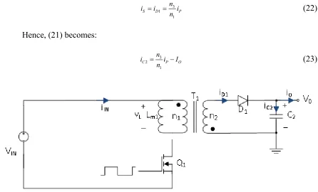
Hence, (21) becomes:
3
2 1
C P O
n
i i I
n
(23)
During the interval tOFF2:
As described earlier in this chapter, tOFF2 is defined as half of T1’s magnetizing and
leakage inductances’ resonance with the combined capacitance at the node of Q1’s drain.
Rewriting equation (5), an expression for tOFF2 is achieved:
2 1 1
1 2
OFF RES m S
t t L C (24)
As illustrated in Fig. 2.5(c), neither Q1 nor D1 are conducting during this period.
Hence,
0 L
v (25)
0 IN
i (26)
2
C o
i I (27)
Fig. 2.6 illustrates the current waveforms of the primary and secondary of transformer
T1 during the period TS. IPP is defined as the peak primary current and ISP is the peak
secondary current. During the tON interval, with a proper transformer design, the primary
current increases linearly from zero to IPP. Throughout such interval, the voltage across the
primary winding isVINVQ ON1, . Therefore;
1,,
1
( IN Q ON)ON PP
m
V V t
I
L
(28)
Furthermore, the energy stored in the primary inductance of transformer T1 (WP)
during tON is given by:
2
1 1
( )
2
P m PP
W L I (29)
Since the input power (PIN) is a function of the energy and the operating frequency,
where;
PIN W fP (30)
Consequently,
2
1
1 ( )
2
IN m PP
P L I f (31)
Combining equations (28) and (31) leads to an expression for the input power in
terms of the operating frequency, input voltage, ON time of Q1, and the primary inductance:
1, 2 2
1
( ) ( )
2
IN Q ON ON IN
m
f V V t
P
L
(32)
Equation (32) could also be rewritten as an expression for tON:
1 1, 2 1 ( ) m IN ON
IN Q ON
L P t
V V f
(33)
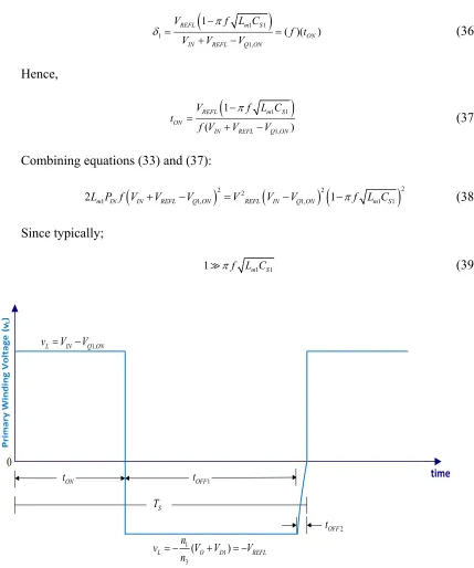
On the other hand, Fig. 2.7 illustrates the primary winding voltage waveform.
It is inherent that the core of the transformer in a flyback operating in the boundary
conduction mode resets to zero during each cycle. For the reset to occur, equal volt seconds
must be applied to the core during the ON and OFF times of Q1. Therefore, from the
volt-second balance equation, where the primary winding voltage (vL) is approximated to zero
during tOFF2, hence;
1(VIN VQ ON1, ) 1'VREFL 1"( 0) 0
(34)
Manipulating equations (13) and (34);
3 1 S P n i i n P i P P I SP I ON
t tOFF1 tOFF2
S
T

![Figure 1.2: U.S. PV installations, Q2 2010-Q2 2014. [3]](https://thumb-us.123doks.com/thumbv2/123dok_us/1325866.1165492/23.612.100.530.429.679/figure-u-s-pv-installations-q-q.webp)


![Figure 2.2: Novel Low Cost PV Converter (or Micro-Inverter) Based on Analog Interleaving Method [5]](https://thumb-us.123doks.com/thumbv2/123dok_us/1325866.1165492/42.612.106.518.213.601/figure-novel-converter-micro-inverter-analog-interleaving-method.webp)
![Figure 2.3: Detailed operation of the proposed scheme [5].](https://thumb-us.123doks.com/thumbv2/123dok_us/1325866.1165492/46.612.118.514.112.687/figure-detailed-operation-proposed-scheme.webp)
![Figure 3.2: Ferrite material loss curves as provided by EPCOS [25].](https://thumb-us.123doks.com/thumbv2/123dok_us/1325866.1165492/75.612.95.518.70.673/figure-ferrite-material-loss-curves-as-provided-epcos.webp)