ISSN (Print) : 2320 – 3765 ISSN (Online): 2278 – 8875
I
nternational
J
ournal of
A
dvanced
R
esearch in
E
lectrical,
E
lectronics and
I
nstrumentation
E
ngineering
(A High Impact Factor, Monthly, Peer Reviewed Journal)
Website: www.ijareeie.com
Vol. 7, Issue 2, February 2018
Analysis of Area and Power Optimization
Techniques for Increased Efficiency of Carry
Select Adder
V.Thilakrathi1, Lavanya .P2, D.Mythili3, Madhu Preetha V4
ASP, Dept. of ECE, MNM Jain Engg College, Thoraipakkam, Chennai, India1
ASP, Dept. of ECE, MNM Jain Engg College, Thoraipakkam, Chennai, India2
ASP, Dept. of ECE, MNM Jain Engg College, Thoraipakkam, Chennai, India3
Student, MNM Jain Engg College, Thoraipakkam, Chennai, India4
ABSTRACT: In this paper the proposed Carry Select Adder (CSLA) design is used to generate the carry and sum which improves the carry propagation delay problems and reduces the area and power consumption. A new logic is proposed which is used to reduce the power and area consumption. Hence the main objective of this work is to reduce the area, power and design complexity using CSLA architecture which optimizes the area and the power.Also the CSLA structure improves the performance of the system. Thus the comparison between the new CSLA and the existing CSLA is done.
KEYWORDS: Area-efficient, low power, CSLA, BEC.
I. INTRODUCTION
The power, area and performance are said to be the major concerns of the VLSI design.Since VLSI designs havevery low power consumption and effective area they are being used in many day to day applications like personal work stations, sophisticated computer graphics and also in multi- media capabilities such as real time speech recognition, video compression technique and real time face recognition systems. The challenges previously faced by the VLSI designers were to increase the performance of the digital system. This necessity actually leads to increase in the demand of portable application and reduce the inefficient use of energy required for electronic devices.
An important component used in the VLSI design is an arithmetic unit which consists of an adder. The adders are the main component in all microprocessors, multiplexers and digital signal processing chip. The microprocessor can execute millions of instructions per second, in which the operating speed of an adder is defined as a major constrain. Despite the fact that adders have the features of VLSI structures in terms of power and area, the performance of an adder islimited by the carry propagation delay.
ISSN (Print) : 2320 – 3765 ISSN (Online): 2278 – 8875
I
nternational
J
ournal of
A
dvanced
R
esearch in
E
lectrical,
E
lectronics and
I
nstrumentation
E
ngineering
(A High Impact Factor, Monthly, Peer Reviewed Journal)
Website: www.ijareeie.com
Vol. 7, Issue 2, February 2018
II. LITERATURE SURVEY
The literature survey describes about power compiler which is a gate-level power optimization and synthesis system. This paper describes about the recent research in power optimization which has produced several algorithms, however, each algorithm is focused on one aspect of the whole power equation. This paper describes a commercial tool capable of optimizing power at the gate-level in addition to performing area and timing optimization. A power analysis engine that models all aspects of power consumption is integrated into the optimization tool so that all aspects of power are considered. Experimental results show an average 11.46% reduction on industrial circuits with a peak reduction of 66.62%. All delay constraints are met and an average 9.41% increase in area is observed. Hence to avoid this we go for the design of new CSLA adder described below
III. DESIGN OF NEW CSLA ADDER
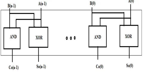
The CSLA adder design of the proposed work is presented in Figure 1 which consists of 4 different unitsgiven ashalf sum generation unit, full sum generation unit, carry generation unit and carry selection unit.
Figure 1. Area- Power optimization CSLA block diagram
In half sum generation unit ,the half sum word (So) and half carry word (Co) of width n-bit each is generated by receiving the two n- bit operands.
ISSN (Print) : 2320 – 3765 ISSN (Online): 2278 – 8875
I
nternational
J
ournal of
A
dvanced
R
esearch in
E
lectrical,
E
lectronics and
I
nstrumentation
E
ngineering
(A High Impact Factor, Monthly, Peer Reviewed Journal)
Website: www.ijareeie.com
Vol. 7, Issue 2, February 2018
Figure 2. (b) Diagram of Carry Generation Unit considering Cin =0.
Figure 2. (c) Diagram of Carry Selection Unit
\
ISSN (Print) : 2320 – 3765 ISSN (Online): 2278 – 8875
I
nternational
J
ournal of
A
dvanced
R
esearch in
E
lectrical,
E
lectronics and
I
nstrumentation
E
ngineering
(A High Impact Factor, Monthly, Peer Reviewed Journal)
Website: www.ijareeie.com
Vol. 7, Issue 2, February 2018
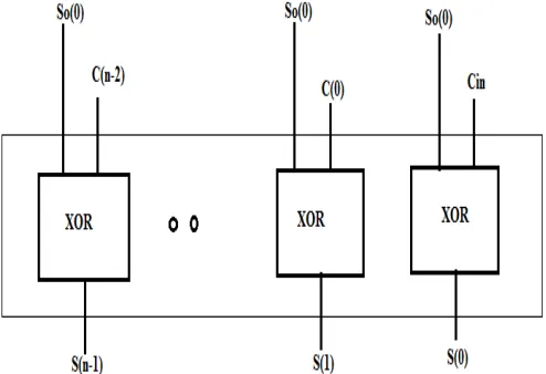
From the half sum generation unit, the carry generation (CG)unit receives both the half sum and half carry word and generate the n- bit carry word C10 corresponding to the input carry 0. The optimized design of carry generation unit is shown in figure 2(b). The carry selection (CS) unit is used to select S one final carry word using the control signal Cin,which receives the half sum and half carry word. The carry selection unit select the carry word C10 from carry generation unit CG0 when Cin = 0. When Cin = 1, from the carry generation unit CG1, this unit selects the carry word . The logic diagram for carry selection unit is shown in figure2(c). The most significant bit obtained from the carry selection unit is The final carry word Cout. In the full sum generation unit,XOR-d to generate the (n -1) most significant bit of final sum S from the remaining(n – 1) bit and (n – 1) bit of half sum word .The logic diagram of full sum generation unit is shown in figure 2(d).
IV. PERFORMANCE ANALYSIS
SCREENSHOTS:
The power and transient response of 4- bit and 8- bit Area-Power –optimization CSLA .
Figure 3. Schematic of 4- Bit Area-Power – optimization CSL
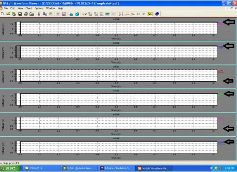
Figure 4. Transient Response of 4- BitArea- power- optimization CSLA .
ISSN (Print) : 2320 – 3765 ISSN (Online): 2278 – 8875
I
nternational
J
ournal of
A
dvanced
R
esearch in
E
lectrical,
E
lectronics and
I
nstrumentation
E
ngineering
(A High Impact Factor, Monthly, Peer Reviewed Journal)
Website: www.ijareeie.com
Vol. 7, Issue 2, February 2018
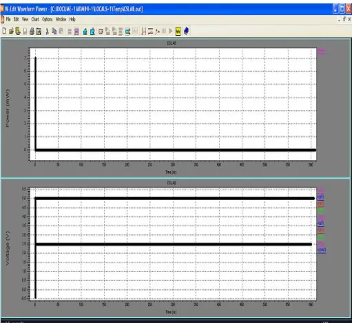
Figure 5. Power Response of 4- Bit Area- Power optimization CSLA.
ISSN (Print) : 2320 – 3765 ISSN (Online): 2278 – 8875
I
nternational
J
ournal of
A
dvanced
R
esearch in
E
lectrical,
E
lectronics and
I
nstrumentation
E
ngineering
(A High Impact Factor, Monthly, Peer Reviewed Journal)
Website: www.ijareeie.com
Vol. 7, Issue 2, February 2018
Figure 7.Transient Response of 4- Bit Area- power-optimization CSLA
Figure 8. Power response of 8- bit Area- Power- optimization CSLA.
ISSN (Print) : 2320 – 3765 ISSN (Online): 2278 – 8875
I
nternational
J
ournal of
A
dvanced
R
esearch in
E
lectrical,
E
lectronics and
I
nstrumentation
E
ngineering
(A High Impact Factor, Monthly, Peer Reviewed Journal)
Website: www.ijareeie.com
Vol. 7, Issue 2, February 2018
V. PERFORMANCE COMPARISON
Based on the factors such as area and power,thecomparison of the proposed CSLA design with the old existing system is tabulated (table I and table II).
From the table I and II , it is thus proven that the area and power consumed by the Area- Power- Optimization CSLA is less when compared with existing CSLA designs.
VI. CONCLUSION
The practical implementation results of an Area – Power –Optimization CSLA in both 4- bit and 8- bit is designed and implemented using Tanner 14.1 EDA tool to demonstrate the reduction in Area and Power and Complexity. It is achieved using optimized logic units together with separate generation of the various carries. Using the control input, one of the carry is selected to produce the final sum and carr.Thus, we reduce the adder carry propagation delay in the design. Also the comparison of the proposed and the existing design in terms of area and power is made. A considerable power and area reduction is noticed in the proposed system than in the existing design. The rest of the work can be preceded and implemented as future work.
ACKNOWLEDGMENTS
It is to acknowledge that this work is carried out by utilizing the resources that is funded by the Electronics and Communication Engineering department, MNM Jain Engineering College, Chennai.
REFERENCES
[1] AkhileshTyagi, ‘A Reduced Area Scheme for Carry- Select Adders’, IEEE transaction on computer, Vol. 42, Pp. 1163 – 1170, 1993.. [2] Bedrij.O.J,‘Carry Select Adder’, IRE Transaction Electronics Computer, Vol.11, Pp. 340- 344, June 1962.
[3] Chang. T.Y and Hsiao.M. J, ‘Carry Select Adder using Single Ripple Carry Adder’, Electronics Letters, Vol. 34, Pp. 2101 – 2103, October 1998. [4] Chyn Wey .I, Cheng Chen, Yi. Sheng Lin and Chin Chang pengl,‘ An Area- Efficient CSLA Design by Sharing the Common Boolean Logic Term’, International Multi conference of Engineers and Computer Scientists, Vol.2 , Pp. 14 -16, March 2012.
[5] He .Y, Chang C.H and Gu.J, ‘An Area Efficient 64-bit Square Root Carry Select Adder for Low power Application’, IEEE International Symposium Circuits Systems, Vol.4, Pp. 4082 – 4085, 2005.
ISSN (Print) : 2320 – 3765 ISSN (Online): 2278 – 8875
I
nternational
J
ournal of
A
dvanced
R
esearch in
E
lectrical,
E
lectronics and
I
nstrumentation
E
ngineering
(A High Impact Factor, Monthly, Peer Reviewed Journal)
Website: www.ijareeie.com
Vol. 7, Issue 2, February 2018
[7] J. P. Fishburn, A. E. Dunlop, "TILOS: a posynomial programming approach to transistor sizing", Proc. ICCAD'85, pp. 326-328.
[8] S. S. Sapatnekar, V. B. Rao, P. M. Vaidya, S. M. Kang, "An exact solution to the transistor sizing problem for CMOS circuits using convex optimization", IEEE Trans. Computer-Aided Design, vol. 12, no. 11, Nov. 1993.
[9] M. R. C. M. Berkelaar, J. A. G. Jess, "Gate sizing in MOS digital circuits with linear programming", Proc. EDAC'90, pp. 217-221. [10] G. Chen, H. Onodera, Κ. Tamaru, "An iterative gate sizing approach with accurate delay evaluation", ICCAD95, pp. 422-427.
[11] S. Perremans, L. Claesen, H. DeMan, "Static Timing Analysis of Dynamically Sensitizable Paths", 26th Design Automation Conference, pp. 568-573, 1989.
[12] P. McGeer, R. Brayton, "Efficient Algorithms for Computing the Longest Viable Path in a Combinational Network", 26th Design Automation Conference, pp. 561-567, 1989.
[13] D. Brand, V. Iyengar, Timing Analysis using Functional Analysis, 1986.