A High-Speed Data Transmission of an Redundant Signed
Digit -Based Ecc Processor
Shaik Farheen & S. V. Ravi Kumar
1 PG Scholar, Dept of ECE, Rise Krishna Sai Gandhi Group of Institutions, Ongole, AP, India.
2Associate Professor, Dept of ECE, Rise Krishna Sai Gandhi Group of Institutions, Ongole, AP, India.
ABSTRACT: In this paper, an exportable
application-specific instruction-set elliptic
curve cryptography processor primarily
based on redundant signed digit illustration
is proposed. The processor employs
extensive pipelining techniques for
Karatsuba–Ofman approach to obtain
excessive throughput multiplication.
Furthermore, an efficient modular adder
without comparison and a high throughput
modular divider, which results in a short
data-path for maximized frequency, are
implemented. The examination of speed and
area overhead among various ECC plans
legitimizes the cost-adequacy of the
proposed ECC architecture with its design
procedure. The Xilinx virtex 5 field
programmable gate array has been utilized.
The usefulness of the FPGA will be checked
by utilizing chip scope pro analyzer. Further
the processor is actualized in ASIC CMOS
innovation.
Index Terms—Application-specific
instruction-set processor (ASIP), elliptic
curve cryptography (ECC),
field-programmable gate array (FPGA),
Karatsuba–Ofman multiplication,
redundant signed digit (RSD).
I. INTRODUCTION
Elliptical curve cryptography (ECC) is an
asymmetric cryptographic device that offers
an equal security to the famous Rivest,
Shamir and Adleman machine with a lot
smaller key sizes. The fundamental
operation in ECC is scalar factor
multiplication, in which a point on the curve
is improved by means of a scalar. A scalar
factor multiplication is performed with the
aid of calculating series of factor additions
and point doublings. Using their geometrical
properties, factors are added or doubled via
series of additives, subtractions,
multiplications, anddivisions in their
respective coordinates. Point coordinates are
top or an irreducible polynomial. Various
ECC processors had been proposed within
the literature that both goal binary fields top
fields or dual subject operations.Carry good
judgment or embedded virtual sign
processing blocks inside Field
programmable gate arrays (FPGAs) are also
applied in a few designs to deal with the
bring propagation hassle. It is important to
construct a green addition facts course in
view that it is an essential operation
employed in different modular arithmetic
operations.In order to optimize the
multiplication method, a few ECC
processors use thedivide and conquer
approach of Karatsuba of man
multiplications, where others use embedded
multipliers and DSP blocks inside FPGA
fabric. In high subject ECC processors,
bring unfastened arithmetic is necessary to
avoid prolonged information paths as a
result of bring Propagation.
Modular multiplication is a crucial
operation in ECC processor. There are two
kinds one is as interleaved modular
multiplication the use of Bernard Law
Montgomery’smethod when arbitrary curves
are required and some other is
multiplythen-reduce and is used in elliptic curves
constructed over finite fields of
Messeneprimes which let in green modular
reduction thru series of additions and
subtraction. Since modular department in
affine coordinates is a costlyprocess,
different techniques are proposed to
compensate the price like jacobian
co-ordinate and fermat’s little theorem. ECC
processor also uses GSD set of rules. Hence,
many ECC processors with combined
modular division and multiplication blocks
were proposed.The complexity of modular
division algorithms is approximately O (2n),
wherein n is the size of operands and the
strolling time is variable and relies upon
immediately on the inputs.
II. RELATED WORK:
Elliptic curve cryptography:
It is a public key cryptography based totally
on algebraic shape of elliptic curves over
finite fields and requires smaller keys to
provide equal security. For present day
cryptographic functions, an elliptic curve is
a plane curve over a finite field which
includes points enjoyable the equation
The smoothness of the curve and distinct
roots are guaranteed by 4𝑎 3 + 27𝑏 2 ≠
0.Point coordinates are of type integers for
an elliptic curve defined by above equation
and are the elements of an underlying finite
field with operations performed modulo a
prime number. Such elliptic curves are
known as prime field elliptic curves.
Redundant Signed Digits
The RSD representation is a carry free
arithmetic where integers are represented by
the difference of two other integers. An
integer X is represented by the difference of
its x+ and x−components, where x+ is the positive component and x−is the negative
component. The nature of the RSD
representation has the advantage of
performing addition and subtraction without
the need of the two’s complement
representation. On the other hand, an
overhead is introduced due to the
redundancy in the integer representation;
since an integer in RSD representation
requires double wordlength compared with
typical two’s complement representation. In
radix-2 balanced RSD represented integers,
digits of such integers are 1,0 or -1.
Karatsuba–Ofman Multiplication:
The complexity of the regular multiplication
using the schoolbook method is O(n2).
Karatsuba and Of man proposed a
methodology to perform a multiplication
with complexity O(n1.58) by dividing the
operands of the multiplication into smaller
and equal segments. Having two operands of
length n to be multiplied, the Karatsuba–
Ofman methodology suggests to split the
two operands into high-(H) and low-(L).The
original Karatsuba algorithm is performed
recursively, where the operands are
segmented into smaller parts until a
reasonable size is reached, and then regular
multiplications of the smaller segments are
performed recursively.
III. PROPOSED SYSTEM:
Due to the dangers of long variety
information paths and brief frequency
variety in present current systems, a way is
proposed to boom frequency variety and
decrease the data path variety. This paper
proposes a new RSD-based high subject
ECC processor with high-pace running
frequency.The processor is a
utility-particular education-set processor type to
provide programmability and
overall performance of left-to-right scalar
factor multiplication algorithm; however,
the ASIP characteristic of the processor
allows extraordinary algorithms to be
performed via the thru examine-best
reminiscence (ROM) programming. The
universal processor architecture is of
ordinary go bar type with 256 digit huge
information buses. The layout method and
optimization strategies are focused in the
direction of efficient individual modular
arithmetic modules in preference to the
general architecture. Such architecture
permits for clean alternative of man or
woman blocks if distinct algorithms or
modular arithmetic techniques are preferred.
Different efficient architectures of person
modular mathematics blocks for diverse
algorithms are proposed. The novelty of our
processor evolves round the subsequent.
1) We introduce the first FPGA
implementation of RSD-based ECC
processor.
2) Extensive pipelining and optimization
strategies are used to acquire a
high-throughput iterative Karatsuba multiplier
which lead to a performance improvement
of just about a hundred% over the processor
proposed in.
3) To the best of our expertise, the proposed
modular department/inversion is the
quickest to be accomplished on FPGA tool.
This is executed through a new green binary
GCD divider architecture based on easy
logical operations.
4) A modular addition and subtraction is
proposed without contrast.
5) Most importantly, exportable layout is
proposed with specially designed multipliers
and conveys unfastened adders that provided
in aggressive results against DSPs and
embedded multipliers-based designs.
IV. OVERALL PROCESSOR
ARCHITECTURE
The proposed P256 ECC processor consists
of AU of 256 RSD digits wide, an
finite-state machine (FSM), memory, and two data
buses. The processor can be configured in
the pre synthesis phase to support the P192
or P224 NIST recommended prime curves
processor architecture. Two sub control
units are attached to the main control unit as
add-on blocks. These two sub control units
doubling, respectively. Different coordinate
systems are easily supported by adding
corresponding sub control blocks that
operate according to the formulas of the
coordinate system.
External data enter the processor through the
external bus to the 256 RSD digits input bus.
Data are sent in binary format and a binary
to RSD converter stuffs zeros in between the
binary bits in order to create the RSD
representation. Hence, 256-bits binary
represented integers are converted to
512-bits RSD represented integers. To convert
RSD digits to binary format, one needs to
subtract the negative component from the
positive component of the RSD digit.
Fig.1. Overall processor architecture
ARITHMETIC UNIT
The AU is the core unit of the processor that
includes the following blocks:
1) Modular addition/subtraction block
2) Modular multiplication block and
3)Modular division block.
A. Modular Addition and Subtraction
Addition is used in the accumulation process
during themultiplication, as well as, in the
binary GCD modular divider algorithm. In
the proposed implementation, radix-2 RSD
representation system as carry free
representation is used. In RSD withradix-2,
digits are represented by 0, 1, and −1, where
digit 0is coded with 00, digit 1 is coded with
10, and digit −1 iscoded with 01.An RSD
adder is presented that is built from
generalized full adders. The problem with
this adder is that it tends to expand the
addition result even if there is no overflow,
since it restricts the least significant digit
(LSD) to be digit −1 only. This unnecessary
overflow affects the reduction process later
and produces some control complexities in
the overall processor architecture.
However,the overflow is easily managed
when the adder is instantiated as a sub block
in the proposed implementation.In order to
overcome the problem of overflow
introduced a method is proposed consists of
two layers, where layer 1 generates the carry
and the interim sum, and layer 2 generates
the sum, as shown
Fig.2.RSD adder/subtractor
The advantage of the proposed modular
addition scheme is that only the MSD digits
of the intermediate results are checked for
the reduction process. Our modular
adder/subtractor consists of one full word
RSD adder, two full word multiplexers, and
one register with some control signals. One
modular addition/subtraction is performed
within one, two, or three clock cycles as per
the value of the MSD that is retrieved after
every addition.
Fig.3. Modular addition subtraction block
diagram
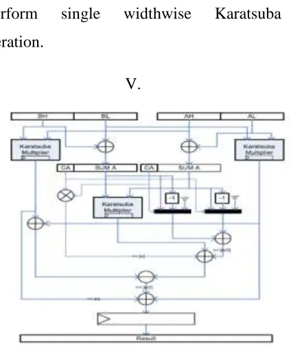
Modular Multiplication
Karatsuba’s multiplier recursive nature is
considered a major drawback when
implemented in hardware. Hardware
complexity increases exponentially with
thesize of the operands to be multiplied. To
overcome this drawback, Karatsuba method
is applied at two levels. A recursive
Karatsuba block that works depthwise, and
an iterative Karatsuba that works widthwise.
The proposed method consists of two
phases: 1) in phase 1, a regular recursive
Karatsuba is built through recursive
construction down to 1-digit level and 2) the
recursive Karatsuba block is used to perform
Karatsuba multiplications iteratively. Hence,
perform single widthwise Karatsuba
iteration.
V.
Fig.4. Karatsuba recursive block diagram
V. CONTROL UNIT AND
INSTRUCTION SET
The control unit consists of the main
controller of the processor that is an FSM. It
also includes two processing units that
control the procedures for the point doubling
and point addition. In order to process the
different coordinate systems, the other
processing units can be generated to support
them as an add-on feature. Hence, new
instructions need to be added to the
instruction set to accommodate the new
processing units. Different scalar point
multiplication algorithms are supported at
instruction level. Different projective
coordinate systems and point
addition/doubling variations are configured
at the control level through add-on
processing units. On the other hand, elliptic
curves with different finite fields are
supported as a resynthesize process.
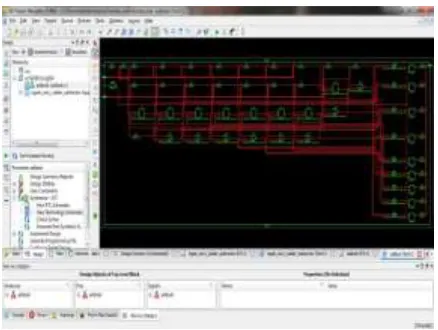
VI. SIMULATION RESULTS
Fig 5: simulation result of the proposed
Fig 6: RTL schematic of the proposed
system
Fig 7: Technology schematic of the
proposed system
VII. CONCLUSION
In this paper, a NIST 256 prime field
ECC processor implementation in FPGA has
been presented. An RSD as a carry free
representation is utilized which resulted in
short data paths and increased maximum
frequency. We introduced enhanced
pipelining techniques within Karatsuba
multiplier to achieve high throughput
performance by a fully LUT-based FPGA
implementation. An efficient binary GCD
modular divider with three adders and
shifting operations is introduced as well.
Furthermore, an efficient modular
addition/subtraction is introduced based on
checking the LSD of the operands only. A
control unit with add-on like architecture is
proposed as a configurability feature to
support different point multiplication
algorithms and coordinate systems. The
implementation results of the proposed
processor showed the shortest data path with
a maximum frequency of 160 MHz, which is
the fastest reported in the literature for ECC
processors with fully LUT-based design. A
single point multiplication is achieved by the
processor within 2.26 ms, which is
comparable with ECC processors that are
based on embedded multipliers and DSP
blocks within the FPGA. The main
advantages of our processor include the
exportability to other FPGA and ASIC
technologies and expandability to support
different coordinate systems and point
multiplication algorithms.
REFERENCES
[1] N. Koblitz, ―Elliptic curve cryptosystems,‖ Math. Comput., vol. 48,no. 177, pp. 203– 209, Jan. 1987.
[3] C. Rebeiro, S. S. Roy, and D. Mukhopadhyay, ―Pushing the limitsof high- speed GF(2m) elliptic curve scalar multiplication on FPGAs,‖in Proc. Cryptograph. Hardw.Embedded Syst. (CHES), vol. 7428.Jan. 2012, pp. 494–511.
[4] Y. Wang and R. Li, ―A unified architecture for supporting operationsof AES and ECC,‖ in Proc. 4th Int. Symp. Parallel Archit., AlgorithmsProgramm. (PAAP), Dec. 2011, pp. 185–189.
[5] S. Mane, L. Judge, and P. Schaumont, ―An integrated prime-field ECDLP hardware accelerator with high-performance modular arithmetic units,‖in Proc. Int. Conf. Reconfigurable Comput. FPGAs, Nov./Dec. 2011,pp. 198–203.
[6] M. Esmaeildoust, D. Schinianakis, H. Javashi, T. Stouraitis, and K. Navi,Efficient RNS implementation of elliptic curve point multiplication overGF(p),‖ IEEE Trans.Very Large Scale Integr. (VLSI) Syst., vol. 21, no. 8,pp. 1545– 1549, Aug. 2012.
[7] D. M. Schinianakis, A. P. Fournaris, H. E. Michail, A. P. Kakarountas,and T. Stouraitis, ―An RNS implementation of an Fpelliptic curve point multiplier,‖ IEEE Trans. Circuits Syst. I, Reg. Papers, vol. 56, no. 6,pp. 1202–1213, Jun. 2009.
[8] J.-W. Lee, S.-C.Chung, H.-C.Chang, and C.-Y. Lee, ―Efficient poweranalysis-resistant dual-field elliptic curve cryptographic processor usingheterogeneous dual-processing-element architecture,‖ IEEE
Trans. VeryLarge Scale Integr. (VLSI) Syst., vol. 22, no. 1, pp. 49–61, Feb. 2013.
Author’s Profile:
SHAIK FARHEEN has received
her B.Tech Degree in Electronic
Communication Engineering from
Pace Institute of Technology and
Sciences affiliated to JNTU Kakinada in 2015
and pursuing M.Tech degree in
VESD(VLSI&ES) in Rise Krishna Sai Gandhi
Group of Institutions, Ongole affiliated to JNTU
Kakinada in 2019, AP, India.
S.V.Ravi Kumar has received
his B.Tech in Electronics &
Communications Engineering
from QIS College of
Engineering & Technology, Ongole, and
M.Tech degree in ES & VLSI from A1 Global
College of Engineering & Technology.
Markapuram, JNTU Kakinada. He is dedicated
to teaching field from last 10+ Years. At present
he is working as Assistant professor in RISE
Krishna Sai Prakasam Group of Institutions,
Ongole, affiliated to JNTU Kakinada in AP,