Abstract
PARK, KIE JIN. Charge defects in low temperature Silicon Nitride/Silicon
Interfaces for Applications in Computational Clothing and Electronic
Textiles. (Under the direction of Dr. Gregory N. Parsons.)
The purpose of this research has been to 1) explore materials prepared using plasma enhanced chemical vapor deposition (PECVD) for amorphous silicon thin film transistors (TFTs) fabricated on large area flexible polyimide substrates, and 2) develop new concepts to make smart fabrics for computational clothing using the flexible TFTs.
effects were believed to be less important than effects of composition change under the conditions studied. Interface charge density increased also with temperature. This was consistent with flat band voltage shift with temperature.
Charge Defects in Low temperature Silicon Nitride/Silicon
Interfaces for Applications in Computational Clothing and
Electronic Textiles
by
KIE JIN PARK
A thesis submitted to the Graduate Faculty of
North Carolina State University
in partial fulfillment of the
requirements for the Degree of
Master of Science
DEPARTMENT OF CHEMICAL ENGINEERING
Raleigh
2002
Approved by
Biography
Acknowledgements
I would like to express my deepest gratitude to my graduate advisor, Dr. Gregory Parsons, for providing me both the direction and the freedom to thoroughly experience the research process, and more importantly, for his endless guidance to help me overcome all the technical obstacles in my thesis. I just want to let me know that he gave me more than enough to do.
I want to thank Kit Yeung who has been a great technical teacher, a great life teacher and a great friend. I would never have been able to complete my reactor repair without his help.
I am also grateful to all the members, past and present, of Dr. Parsons’ research group including Dr. Laura Smith, Dr. Theodosia Gougousi, Atul Gupta, Kevin bray, Dong Niu, Jason Kelly, David Terry, Tom Abatermarco, Powan Mehan, and Changwoong Chu. I am indebted to TFT research group including Kevin bray, Leonard Nelson, and Laura. Special thanks go to Kevin bray for advising research and helping writing thesis and Leonard for excellent contributions to the reactor repair and research.
Table of Contents
List of Tables
.……….……….……… viList of Figures
..……….. viiI.
Introduction
……….…………. 1.1 Background……….…. 21.2 Hydrogenated Amorphous Silicon TFTs……….… 2
1.3 TFT Structures……….… 4
1.4 Silicon Nitride………. … 4
1.5 TFTs on Plastics……….….. 1.6 Electronic fibers and Textile……….... 6
1.7 Application for computational clothing …...………..…. 8
1.8 Technical Challenges………. 10
1.8.1 Electronic fibers ……….………..……….. 1.8.2 Challenges in TFTs ……….……..………. 1.9 Summary………..….…. 14
II.
Experimental
………..…………. 2.1 Materials Preparation……….……….….162.1.1 Silicon nitride capacitors ………..………. 2.1.2 TFTs fabricaion ………. 2.2 Materials Characterization………..……..……….. 19
2.2.1 FTIR measurement ………...…… 2.2.2 Electrical characterization ………..
17
19 19 15
16 15 5 1
2.3 TFTs Charaterization……… 20 2.4 Weaving TFTs and Conductive yarns………..…
III.
Results and discussion of TFT materials and device
…….. 3.1 Effects of deposition conditions on the properties of SiNx………..
3.1.1 Infrared absorption results ……….…………..….... 24 3.1.2 Electrical results ……….……….. 3.1.3 Discussion ………..……... 3.2 TFTs Performance ………..
IV.
Application to woven electronics
……….……… 35 - Woven circuits with TFTs and Conductive yarns ..………..…………. 36V.
Conclusion
………..…...
References
……….…. 4121
24
29 33
38 23
List of Tables
Table I: Deposition conditions for processing gas composition effect
experiments on silicon nitride films ………. 46
Table II: Deposition conditions for temperature effect experiments on
List of Figures
Figure 1: Conventional TFT structures ……….. 48
Figure 2: Tri-layer surface on Kapton® after development ……..………. 49
Figure 3: The fabrication process of TFT on Kapton® ……….…………
Figure 4: Large area showerhead reactor ……….…….………….
Figure 5: Sewing diagram for active woven circuits .……….…………...
Figure 6: Mask design set #1 for TFT ……….…..…….…….…….
Figure 7: Inverter and NOR gate from TFTs on Kapton® and conductive
Threads ………..
Figure 8: Infrared absorption spectra for PECVD SiN
xfilms with different
NH/SiH ratio at T =150
oC ……….… 55
Figure 9: Infrared absorption spectra for PECVD SiN
xfilms with different
NH/SiH ratio at T =250
oC ………. 56
Figure 10: Infrared absorption spectra for PECVD SiN
xfilms with different
Temperature at NH
3/SiH
4= 10 ……….
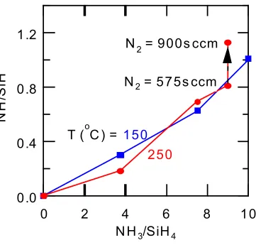
Figure 11: Processing gas composition effect on NH/SiH ………
Figure 12: Total hydrogen concentrations ……….
Figure 13: The deposition rate variation with temperature at NH
3/SiH
4= 10
50
51
52
53
54
……….. 60
Figure 14: Current density vs. electric field for SiN
xwith different NH/SiH
ratio at 250
oC ……..……….. 61
Figure 15: Current density vs. electric field for SiN
xwith different NH/SiH
ratio at 150
oC ……..……….. 62
Figure 16: Current density vs. electric field for SiN
xwith different
temperature at NH
3/SiH
4= 10 ………..………. 63
Figure 17: C/C
oxvs. voltage plots for nitride flims with different NH/SiH
ratio at 150
oC ……… 64
Figure 18: C/C
oxvs. voltage plots for nitride flims with different NH/SiH
ratio at 250
oC ……… 65
Figure 19: C/C
oxvs. voltage plots for nitride flims with different temperature
at NH
3/SiH
4= 10 ………..…. 66
Figure 20: The hysteresis loop for capacitance vs. voltage ……….
Figure 21: Total charge density variation with NH/SiH ………. 68
Figure 22: C/C
oxvs. voltage plots with nitride thickness for various NH/SiH
ratio at T = 150ºC ………….………..…………..…. 69
Figure 23: C/C
oxvs. voltage plots with nitride thickness for various
Figure 24: Plots of flat band voltage versus the nitride thickness …………71
Figure 25: The charge variation in the interface and bulk film with NH/SiH
ratio at 150
oC ……… 72
Figure 26: The charge variation in the interface and bulk film with
temperature at NH
3/SiH
4= 10 ………..
Figure 27: Cross-sectional structure model of the condensation of absorbed
Si(NH
2)
3toward on Si-N network with evolution of NH
3…… 74
Figure 28: Stress in the a-SiN
x:H layer with nitrogen content ………….…75
Figure 29: Drain current versus drain voltage for the TFT on plastic …….
Figure 30: Log of drain current versus gate voltage for the TFT on plastic
……….. 77
Figure 31: mobilities for TFT on plastic ………. 78
Figure 32: Woven circuits for contact measurement ………..
Figure 33: Contact resistance with different materials ………
Figure 34: Resistance vs. Distance for two contacted Kapton strips………
Figure 35: A composition of the respective electrical resistances of five
different conductive fibers ……….
Figure 36: Simple inverter application with TFTs and conductive
yarns ……….…….
76
80
79
81
73
82
Figure 37: Wearable integrated circuit: inverter structure ……….. 84
Figure 38: Mask design set #2 for TFTs ………….……… 85
Figure 39: Electric field vs. Current density for Metal-Insulator-Metal
structure
……… 86
Chapter I.
1.1 Background
Conventional metal-oxide-silicon (MOS) field effect transistors are fabricated on crystalline wafers of silicon cut from a crystal boule grown from a melt. Metal-oxide-silicon field effect transistors thus fabricated have high mobility (~1000 cm2/V•s) and relatively small feature size (~0.18) micrometers. In many applications, electronic devices have to be made on substrate rather than on single crystal silicon1 MOS transistors thus fabricated are usually called thin film transistors (TFTs). Thin-film transistors (TFTs) were proposed by Weimer2, 3 in 1961. For the application in the integrated circuits (IC’s), thin film transistors are used as load devices of static random access memory4. For the application in large area circuits, thin film transistors are used as switches of pixel elements of active matrix liquid crystal displays (AMLCD’s). For the sake of manufacturing cost and ease of fabrication, amorphous silicon thin film transistors (a-Si TFTs) are adopted currently in industry for the manufacturing of active matrix liquid crystal displays. The carrier mobility of amorphous silicon thin film transistors is much lower (0.5 ~1.0 cm2/V•s).
1.2 Hydrogenated Amorphous Silicon TFTs
applications. There are some advantages of a-Si:H7. A-Si:H is usually deposited by plasma enhanced chemical vapor deposition (PECVD) in which silane gas (SiH4) is
decomposed in a plasma excited by rf power. A typical rf frequency is 13.56 MHz, although much lower frequencies (e.g. 100Hz) can also be used. Using this technique, films can be deposited with thickness variations of only a few percent over the entire surface area. A-Si:H film can be deposited at low temperature. Low temperature deposition is essential in the fabrication of active matrix liquid crystal displays because glass or plastics are used as the transparent substrate materials8-11 . The deposition rate must be low because good-quality a-Si:H films can only be formed if hydrogen is incorporated into the amorphous network; hydrogen will not be retained in the film if the substrate temperature is higher than 450 °C. a-Si:H is an amorphous material, so it can easily form hetero-interfaces while maintaining good interface properties. It is possible to deposit amorphous silicon on various substrates such as insulators (including glass, oxides, and nitrides), metal and semiconductors. The interface properties between the a-Si:H and the SiNx gate insulator play a critical role in TFT characteristics. The a-Si:H
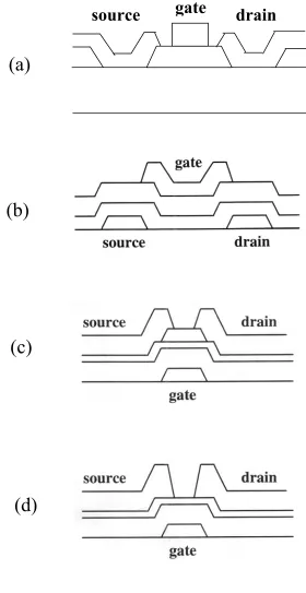
1.3 TFT Structures
The structure of thin film transistors is usually categorized as co-planar type or staggered type12-14 as illustrated in Figure 1. Staggered structure was usually adopted in the fabrication of amorphous silicon thin film transistors while co-planar structure was usually adopted in the polycrystalline silicon thin film transistors. In the staggered structure, there is normal staggered structure, which is usually called “top-gate thin film transistors” and is shown in Fig. 1.1(b), and there are inverted staggered structures, which are as usually called “bottom gate thin film transistors” and are shown in Fig. 1.1(c) and (d). The inverted staggered structure is further categorized as inverted staggered tri-layer configuration (Fig. 1.1(c)) or inverted staggered back channel cut configuration (Fig 1.1(d)). Inverted staggered thin film transistors usually achieve better performance than staggered thin film transistor15. It is generally believed that the sequence of plasma enhanced chemical vapor deposition determines the interfacial property between amorphous silicon and silicon nitride, which to a large extent determine the performance of the device. Plasma enhanced chemical vapor deposition of silicon nitride using silane and ammonia as the source gas mixture inherently needs high rf input power to generate NHn radicals16. And, this partially explains the better device performance of inverted
staggered thin film transistors.
1.4 Silicon Nitride
PECVD silicon nitride (SiNx) has been exclusively used in the fabrication of
crystal displays. SiNx is the preferred gate dielectric material for a-Si:H TFTs because it
gives better device performance than other dielectric such as silicon dioxide. Compared with a TFT with SiNx gate dielectric layer, TFT with SiO2 in the dielectric structure has
inferior switching characteristics because SiNx gives better interfacial qualities17.
However the reason is still not clear. SiNx can be characterized according to its chemical
properties, such as Si/N ratio, Si-H and N-H concentrations, or its characteristics, such as reflective Index, energy gap, dangling bonds, charge density, and stress. They all affect the transistor’s threshold voltage, reliability, on-current and off-current. Good quality, i.e., high breakdown voltages and low leakage current, silicon nitride films can be deposited using SiH4 and NH3 gases or with the addition of N2. It is well known that
silicon nitride films deposited using SiH4, NH3, and N2 gases at high substrate
temperature (>250 oC) have good electrical properties. It was not clear, however, how N2
affects the deposition process. Yue Kuo12 suggested that N2 has the effect of shifting the
electron energy to high energy, thus promoting the dissociation of NH3.
1.5 TFTs on plastics
of amorphous silicon technology in which all processing steps can be routinely carried out at temperatures below 300 °C. Most common polyimides are stable to temperatures approaching 400 °C. So polyimide film or web is being used as a flexible substrate for amorphous silicon ultra thin electronics in a developing technology21. A class of channel length (L) equal to 2-50 µm minimum feature size inverted gate thin film transistor circuitry has been demonstrated, including individual ratio (W/L) from 1 to 1000, inverters, drivers and receivers, ring oscillators, logic circuits and SRAM cells on 5 and 75 µm polyimide substrates22-24. The technology developed is compatible with roll-to-roll processing and mass production and demonstrates the feasibility of TFT based circuits on polyimide comparable to those on rigid substrates.
1.6 Electronic fibers and Textiles
integration is not achieved since the electronics and the cup are two separate entities and the electronics need to be removed for washing the cup. There are also novel approaches towards integration of passive electronic components into objects, such as Post and Orth’s25. They integrated conductive stainless steel fibers into textiles for the purpose of connecting circuit boards and point in the direction of a higher-scale integration. D. De Rossi et al.26 used conductive polymer and conductivity changes on this coating as a function of strain and temperature were observed. A glove prototype made from this coated textile showed sensing and actuation capabilities embedded into a piece of textile. At the micro-scale, Drury et al. reported all polymer microelectronics devices fabricated on the flexible substrates at a low cost using organic semiconductors27. Given today’s technology, it is possible to group the possibilities of the integration of (micro) electronics into clothing at three levels.
1) Garment level integration is the first level. At this level, the fundamental design of clothing and electronics are accomplished independent from each other and are combined at a later stage. A good example of this type of integration is the Philips-Levi’s ICD jacket28.
2) As a second level, the electronics is integrated into the garment. A good example of this level is circuit boards attached onto the fabric connected to each other using conductive threads29. Integration of electronic components, such as sensors and integrated
circuits are also examples that can be included in this group30. This provides a relatively unobtrusive way of integrating electronic components into clothing.
generically defining the geometry of a material having very long length compared to its cross sectional dimensions, i.e. a very high aspect ratio. Fibers are used in many different areas of industry, from textile to optics to advanced composite materials. Simplest example is naturally the textile in the form of clothes, curtains, table clothes or textiles of that sort. Today, fibers in the everyday objects have basically structural and aesthetic functions with a certain macrostructure and appearance. However, “fibers” can also have added functions in the context of “wearable computing” as previously recognized by Post, and Orth25, 30. In terms of the integration of computing power into clothes or entities of that kind, we share the vision that “eventually, whole computers might be made from materials people are comfortable wearing”31. The main concept of “Fiber Computing” is to embed the basic unit of computation, transistor, into fibers that make up the clothes we wear. These transistors then may be connected to form inverters, gates and higher level circuits.
1.7 Application for computational clothing
Wearable computer have great potential for military use, and there is currently great interest in what this device can do. There are several aspects of wearable computers (WC) that relate to their use in the military. They must be rugged, and applicable military standards exist. They may have docking stations, cradles or holsters for recharging, uploading/downloading information, providing communication, or for securing the device and preventing damage. Weight and cost are important. Finally, other features that arise from their mobility requirements include wireless communication and knowledge of current location. One of the commander’s main requirements is communications. That is, he must advise subordinates of changes in mission, support, and threat; also, he must inform superiors of changes in threat or timelines. The wearable computer can simplify this procedure because communication can be facilitated by antenna arrays sewn into clothing associated with the WC, using a WC to update information. Position determination and map functions could be performed by the WC. Medical support and tactical internet application would be effective one.
1.8 Technical Challenges
1.8.1 Electronic fibers
High speed, high performance computation will continue to be dominated by silicon-based microelectronics for the foreseeable future. However, there are many applications that would benefit from the development of large area, lower performance distributed electronics, especially if the substrate were rugged, flexible, and inexpensive. As an example, military applications include active camouflage, inflatable decoys, large area sensors, large area emitters, large area actuators, etc. Regardless of so many potential applications, electronic textiles are not pervasive because there has been little or no work on the development of the building blocks to build even single devices. There are several challenges for this field.
1) Fibers need to be made out of suitable materials that will host the transistors and be flexible. The magnitude and frequency stresses make our clothing suffer especially during maintenance (such as washing).
2) Material selection is important issue for satisfying both adequate electrical (e.g. insulator) and mechanical properties (e.g. compliant). Though transistor fabrication on curved surfaces is not entirely new and several examples already exist32, 33, the basic question is handling of fibers during fabrication and interconnections between the transistors.
characteristics to the fiber. Packaging also certainly plays a crucial role in minimizing the stresses that the core fiber carrying the electronics will experience.
4) Reliability refers to an estimate for the ability of a system to function properly over time. Packaging and reliability are closely related. As fibers will be exposed to maintenance of the garments they are on, time dependent effects will be more significant. Therefore for reliability viewpoint, packaging should be well engineered to protect the fibers while maintaining necessary mechanical properties.
5) Integration of the computing fibers into the textile material and scalability are the factors need to be considered. In a digital clothing application, at the higher level, one can imagine applications where sensors or the processing done on the sensors are not fixed at the specific locations but they need to change over time. Cell matrix or a cell matrix like architecture can facilitate the implementation of wiring between sensors, logic elements, as well as processing of sensor data for presentation or decision-making.
The principle component of any active semiconductor device is the transistor. As a method to make smart fabrics, transistors need to be fabricated on flat yarn ribbons. There are three different semiconductors as potential candidates for transistors on threads; nanocrystalline silicon, amorphous silicon, and organic materials34-37 including pentacene38 (and derivatives). Nanocrystalline silicon is a thin film silicon material grown by plasma enhanced chemical deposition (PECVD). This is the deposition technique used widely for making amorphous silicon films. When PECVD is run using silane (SiH4)
derivatives34-36 and pentacene37 for organic thin film transistors (TFTs), due to their high field effect mobilities observed in these materials and due to intermolecular interactions which lead to larger grain sizes and fewer grain boundaries, facilitating charge transport37, 39, 40. Pentacene films deposited from solution are polycrystalline with grains randomly oriented. The mobility in these films is limited by charge trapping at grain boundaries41. The basic distributed architecture of fabricating TFTs on strips and conductive threads can be driving materials for the circuit architecture by stacking them on each other. This device architecture impacts the circuit styles we use for implementation of logic primitives such as inverter, NOR and NAND gates. Other circuit primitives such as adders, latches, flip-flops, multiplexers and demultiplexers would be configurated using the basic NOR, NAND and inverter gates.
1.8.2 Challenges in TFTs
TFT on flexible substrates is a basic building block of our approach. There are several issues for TFT performance and addressing TFTs with conductive yarns. Two major performances of TFT are the threshold voltage and the mobility. The threshold voltage of a-Si:H TFT is related with the defect density of a-Si:H, the interface density around the Fermi level between SiNx and a-Si:H, and the charge in the SiNx. The mobility of a-Si:H
TFT is related with the band tail states of a-Si:H, the n+ ohmic contact, the thickness of undoped a-Si:H layer and the SiNx/a-Si:H interface. Among these, a-Si:H/gate dielectric
interface, a-Si:H, and SiNx bulk film qualities are key factors affecting TFT performance.
Hydrogen is an important element in thin film transistor (TFT). Since a-Si:H and SiNx
contain approximately 10 and 30 percent of hydrogen, respectively. In a-Si:H and SiNx
film process H2 and NH3 are included in the feed stream which is an additional hydrogen
source for these films. The main function of hydrogen in TFT is to passivate silicon and nitrogen dangling bonds that are charge trapping centers. Plasma hydrogenation process can improve TFT characteristic by the interface hydrogen step. However, the mechanism of the hydrogenation isn’t still well explained. Since a-Si:H is a field effect transistor, the transistor behavior is greatly influenced by a thin electron accumulation layer induced at the interface of gate SiNx and a-Si:H. The interface morphology and electrical properties
are critical to TFTs. A PECVD process contains particles of various forms and energy (e.g., atoms, molecules, radicals, and ions) and short wavelength light. These parameters affect the film’s morphology, surface states, and band structure. In order to prepare a high performance TFT, properties including morphology, chemical structure, physical band energies, density of states, and stress mismatch have to be optimized. Films deposited by plasma enhanced chemical vapor deposition (PECVD) are affected by gas composition and deposition conditions such as RF power, temperature, and pressure. Though it was mentioned in Chapter 1.5 that polyimide film can be processed up to 400oC, thermal responses of polyimide film and silicon nitride film are very different, i.e. polyimide film shrinks upon heating, for example 0.1% for 200ºC 30min and has a thermal expansion coefficient of 20 x 10-6/ºC while the thermal coefficient of silicon nitride film is 1.5 x 10 -6/ºC. Also, the stress of silicon nitride film varies with nitride film deposition
result in a net compressive stress at the substrate/SiNx interface. The stress difference between polyimide film and the silicon nitride will likely lead to defects at the interface, and could lead to film delamination (as shown in Figure 2). So, the effect of temperature on the substrate, and on the deposited film composition, is a significant issue for TFT fabrication on plastic substrates.
Another important issue is the method of interconnecting TFT’s on adjacent fibers within a woven network. To obtained reliable interconnection, issues related to thread/thread and thread/TFT contact resistance should be characterized and understood.
1.9 Summary
The demand for wearable or potable electronic circuits is growing but weaving approach in fabric level with TFTs on plastic film and conductive yarns has not been tried. In this work, a-Si:H TFTs were fabricated on 125 µm polyimide film using back channel cut inverted staggered TFT structure. The gate insulator of SiNx has been studied
with various deposition conditions. It was shown that the PECVD deposition temperatures are related to the bulk and interface charges of the films. NH/SiH ratio in silicon nitride film was characterized by charges in films. TFTs for smart fabric were made with low temperature SiNx, and a-Si:H having acceptable mobility and threshold
Chapter II.
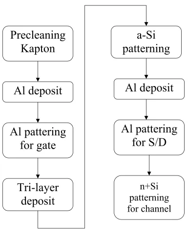
2.1 Materials Preparation
2.1.1 Silicon nitride capacitors
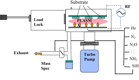
A capacitively coupled rf (13.56 MHz) PECVD system was used for the deposition of various silicon nitride films. The electrode area is 30 x 35 cm2 with a spacing of 3 cm. The system is capable of depositing uniform nitride films over 900 cm2. The process gases were introduced through a showerhead array of 0.5 mm-diameter orifices in the rf-powered electrode. N-type silicon wafers were used as substrates, and their resistivities are about 1.0 Ohm٠cm. Wafers were cleaned by the JTB Baker solution and 1% HF solution before being loaded into the reactor. For silicon nitride characterization experiments, 1) processing gases composition and 2) substrate temperature effects on the properties of the nitride films were studied. For 1) processing gas composition effect experiment, substrate temperature was kept at 150oC or 250oC, and processing pressure was kept at 0.4 Torr. RF power was also kept at 150W. Processing gases composition was controlled with changing NH3/SiH4 ratio while N2 was constant at 575 standard
cubic centimeters per minute (sccm). The summary of the deposition conditions for gas composition effect experiments is shown in Table I. For 2) substrate temperature effect experiment, processing gas composition was kept at NH3/SiH4/N2=7.5/75/575. Both
by evaporation with thickness 2000 Ǻ. For patterning Al, shadow masks whose area is ~7 x 10⁻⁴ cm2 were used during evaporation of Al.
2.1.2 TFTs fabrication
Si:H. Silane with a flow rate of 50 standard cubic centimeters per minute (sccm) and 500, 1500 sccm of hydrogen were used for a-Si:H and n+Si depositions, while a combination of 575 sccm nitrogen, 5 sccm silane, and 75 sccm ammonia was used for SiNx deposition.
The dielectric constant of SiNx was calculated from the characteristic curve of
displacement current versus applied voltage in MIS structures. Processing parameters for doped n+ a-Si:H are same as intrinsic a-Si:H deposition except the silane gas used for processing contained 1 percent of phosphine. After n+ deposition, positive photoresist of one micrometer is applied on top of the trilayer, and ultraviolet light of 275 W is then shined through the printed emulsion mask. After developing the photoresist, reactive ion etch (RIE) was used to form active transistor island area. The RIE process included SF6
and O2 gases. For RIE etching, operating pressure was 60mTorr, RF power was 100W
and Temperature was 20 °C. Etching time for a-Si islands using first mask was 2 min 15 second and 27second for a-Si channel patterning. The following step is contact metal deposition (Al). Deposition conditions are same as those of gate Al but evaporation time. A base pressure of 2x10⁻⁶ Torr is necessary in the evaporator chamber before the aluminum deposition. The contact Al having fin patterns was patterned by conventional photolithography using printed emulsion mask, and wet etched by H3PO4, HNO3 and
CH3COOH mixed aqueous solution. Without removing photoresist, n+Si:H was etched
by reactive ion etch (RIE) processed with SF6 and O2 gases in order to make source/drain
2.2 Materials Characterization
To charaterize silicon nitride layer, FT-IR (Foulier Transform-Infrared) spectra absorption, Capacitance-Voltage, and Current-Voltage measurement were performed.
2.2.1FTIR measurement
Samples deposited on high resistivity (> 10 Ohm ·cm), double-side polished Si (100) substrates were used to perform infrared spectroscopy analysis. The spectra were collected in the transmission mode with a 4 cm-1 resolution using a Nicolet Magma 750. Absorption coefficients can be calculated from absorbance values after subtracting the baseline. No spectral deconvolution was performed.
2.2.2 Electrical characterization
For Capacitance-Voltage (CV) and Current-Voltage (IV) measurement, MIS (Metal Insulator Semiconductor) structures were used. For IV measurement, the gate biased positively, and the ramp rate was 5V/s. For CV measurements, the samples are initially biased to –3 MV/cm and illuminated for 1-2s to create an inversion layer at the substrate/silicon nitride interface. The creation of the inversion layer eliminates deep depletion in the substrate and insures that majority of the applied voltage is dropped across the insulator. Dielectric constants of silicon nitride films can be extracted using an equation as follows:
o nitride
A C
d
ε ε
Cnitride is the capacitance read from the capacitance meter, A is the area of the test dot, d
is the thickness of the silicon nitride film, εo is the permittivity of vacuum, and ε is the
dielectric constant. The dielectric constants for silicon nitride films deposited at 150 oC, 250 oC using SiH4, NH3, N2 gases was calculated from Cox obtained by CV
measurement. The dielectric constants for the films deposited at 150 oC ranged 3.0 to 5.0. The dielectric constants for the films deposited at 250 oC ranged 6.0 to 8.0.
2.3 TFT Characterization
Thin film transistors were characterized using an HP 4145A analyzer by 1) drain current versus gate voltage (Id-Vg), which is usually plotted as log (Id) vs. Vg; and 2)
drain current versus gate voltage (Id-Vd). TFT’s parameters, i.e., threshold voltage,
effective linear mobility, saturation mobility, and subthreshold slope are extracted from Id-Vg measurement. Effective linear mobilities are extracted using the following
equation:
1 1 d
eff
i d g
dI L
W C V dV
µ = ⋅ ⋅ ⋅
(2)
where µeff is the effective linear mobility, L is the channel length, W is the channel
width, and Ci is the capacitance of the gate insulator per unit square (cm2). Vd is kept at
0.1V in measuring the effective linear mobility. To determine the threshold voltage of a thin film transistor, we draw a straight line with the maximum slope on the Id-Vg curve,
curves while keeping Vg=Vd. The expression used to calculate the saturation mobility is
as follows:
2
2 1
g d
d sat
i g V V
d I L
W C dV
µ
=
= ⋅ ⋅
(3)
µsat is the saturation mobility of the measured thin film transistor. The subthreshold slope
of a thin film transistor can be extracted from log (Id) vs. Vg plots. To measure the
subthreshold slope (equation 4), draw a straight line on log (Id)-Vg curves for Vg=0~5V.
The inverse of the slope of this straight is the subthreshold slope, and the unit of the subthreshold slope is V/decade.
(log D)
dVg S
d I
= (4)
The threshold voltage and the subthreshold slope are an indication of the density of states around Fermi-level in the interface between the a-Si:H and a-SiNx layers.
2.4 Weaving TFTs and Conductive yarns
was measured by distance variation with various metal contact. General volt-meter was used for measuring device. Pressure was applied at Al strip contact point. Contact resistance was extracted from equation (4).
T C
d
R R
A
ρ
= + (5)
RT, RC, ρ, A and d are total measured resistance, contact resistance, resistivity of metal,
area of contact and distance.
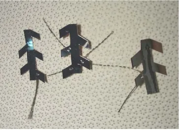
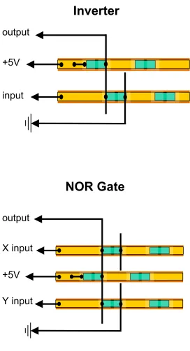
TFTs prepared on Kapton® film was weaved with conductive thread. Fin areas in the top view of TFTs were prepared for sewing TFT and threads (Figure 5), while maintaining contact for source and drain. By designing unique masks design (Figure 6) and processing (Figure 3), TFT structure can prevent from short with contact and gate. To apply TFT on Kapton® to general electronic circuits, by using sewing method, Inverter and NOR gate were prepared. The Inverter and NOR gate are shown in Figure 7.
Chapter III.
Results and discussion
3.1 Effects of deposition conditions on the properties of SiNx
3.1.1 Infrared absorption results
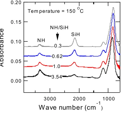
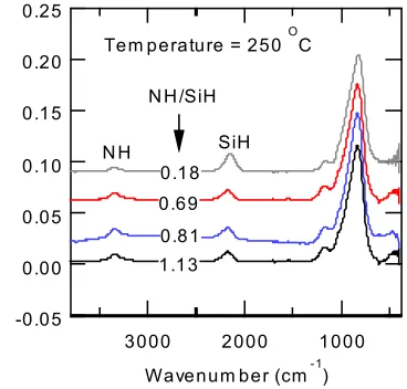
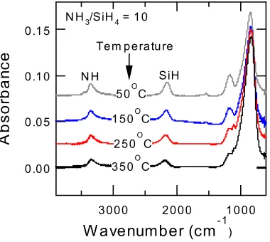
The effects of substrate temperature and source gas composition were investigated in relation to silicon nitride film structure. The infrared absorption spectra of silicon nitride film deposited with various NH3/SiH4 ratios at 150°C and 250°C are shown in
Figure 8 and 9, respectively, and Figure 10 shows the infrared absorption spectra for various temperatures when NH3/SiH4 ratio is fixed at 10/1. Peaks of infrared absorption
are assigned as follows, 1) N-H stretching mode at 3300 cm-1, 2) Si-H stretching mode at 2140 cm-1, and 3) N-H2 scissors at 1550 cm-1. The integrated absorption of N-H and
Si-H stretching bands are correlated with the atomic concentration of hydrogen, which were calculated using the method proposed by Lanford and Rand43. Figure 11 shows
the NH/SiH ratio obtained from the spectra in Figures 8, 9 and 10 plotted vs. NH3/SiH4
gas phase ratio. The figure shows that the NH/SiH ratio increases with increasing NH3/SiH4 ratio, and the trend is similar for films deposited at 150 and 250°C. This
trend is consistent with other group’s work44, 45. Figure 11 also shows that NH/SiH ratio increases with increasing N2 flow rate. This suggests that nitrogen dilution has an
‘extra’ effect of enhancing the NH/SiH ratio of nitride film. Yue Kuo46 concluded that
nitrogen acts as an energy booster, which enhances dissociation of both SiH4 and NH3
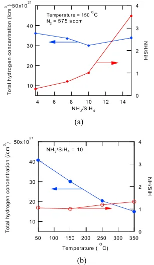
Figure 12 (a) shows NH/SiH ratio and total hydrogen concentration, [H], calculated from the data in Figures 9 plotted vs. NH3/SiH4 flow ratio, and Figure 12(b) shows a
substrate temperature. We note that the total hydrogen content is sensitive to temperature but independent of flow ratio, whereas the NH/SiH ratio is sensitive to flow ratio but not temperature. The decrease [H] with temperature is likely linked to the fact that the deposition rate tends to decrease with increasing temperature, as shown in Figure 13.
3.1.2 Electrical results
The silicon nitride films described above were also electrically characterized. Figure 14 and 15 are logarithmic plots of current density versus electric field measured at room temperature for nitride films deposited at 150°C and 250°C, respectively, with different NH/SiH ratios. Figure 14 and 15 show that leakage current generally decreases with increasing NH/SiH ratio for films deposited at 150 and 250°C. Figure 16 is current vs. voltage for silicon nitride films deposited with different temperature for a fixed NH3/SiH4 ratio (ratio = 10), corresponding to a fixed NH/SiH ratio in the
films (NH/Si-H ≈ 1). It is interesting to note that the leakage current between 4 and 10 MV/cm appears to improve with decreasing substrate temperature. Capacitance-Voltage analysis was also performed on these films, and results are shown in Figures 17-20. Figure 17 and 18 show the effect of NH/SiH ratio on flatband voltage for films deposited at 150 and 250°C respectively. We find that the flatband voltage is shifted negative from the expected VFB (-0.04 V for Al gate electrodes) for both 150 and 250°C
than for the film with NH/SiH = 1.0. Figure 19 is capacitance versus voltage for different temperatures at NH3/SiH4 =10. All films show negative shift, consistent with
positive fixed charge, but the magnitude of the shift decreases with decreasing film deposition temperature. Figure 20 (a) and (b) show CV curves for films deposited at 150 and 250°C. The hysteresis sweep direction (negative ∆VFB) indicates that holes
were injected into the nitride from the substrate and trapped during the CV cycle. The total trapped charge in the dielectric layer can be estimated from the CV flatband voltage shift using equations (6) and (7)47.
1 136 / 300 1 FB OX OX A C C T t N = + (6)
In equation (6), CFB is flatband capacitance, and NA is the substrate doping
concentration. Equation (6) gives us the point on the CV curve (relative to Cox) that
corresponds to flatband. We then use the value of CFB/COX to read VFB from the CV
curve, and input VFB into equation (7) to obtain QT.
( MS FB) OX o
T OX V K Q t φ − ε
= (7)
In equation (7) VFB is flatband voltage, ΦMS is work function difference between
metal and the semiconductor, Kox is nitride dielectric constant obtained by Cox from CV
density in the film, corresponding to a sum of the positive and negative fixed and bulk charge. If positive and negative charges are present in equal amounts (i.e. negative at the interface and positive in the film bulk), then the net charge density, QT, will be zero.
Bulk and interface charges can be deduced by measuring the thickness dependence of Vfb, as discussed below.
Results of total net charge density obtained from the CV data in Figures 17 and 18 are shown in Figures 21. Figure 21 shows the total charge density plotted vs. NH/SiH ratio. The smallest charge densities are observed at low NH/SiH, but these films show high leakage in the IV traces (Figures 14 and 15). The highest charge densities are observed for NH/SiH near 1.0, with decreasing net charge as NH/SiH increases above 1. Note that the net charge density increases somewhat with increasing substrate temperature.
By characterizing the thickness dependence of CV curves and flatband voltage shifts, the total charge distribution (i.e. interface vs. bulk charge) can be determined. For a fixed charge density in a film, increasing the film thickness leads to an increase in the total charge, and therefore an increase in the VFB shift. However, if the charge
density is located primarily at or near the silicon/dielectric interface, increasing film thickness will not change the total charge density. However, we still expect a change in VFB with thickness because Cox changes as film thickness changes. Therefore,
considering bulk (QBC) and interface (QIC) charges, the measured flatband voltage will
2
2
IC BC
FB MS OX OX
S o S o
Q Q
V t t
K K
φ
ε ε
= − − (8)
This relationship holds only for QBC distributed uniformly through the film bulk.
Figure 22 and 23 show CV curves measured at various film thicknesses ranging from 400 to 1500 Å. Figure 24 (a) shows the effect of film thickness on VFB obtained from
CV analysis for films deposited with various NH/SiH ratios at 150°C. Figure 24 (b) is a similar set of plots for films with NH3/SiH4 = 10 (i.e. NH/SiH ≈ 1.0) deposited at
temperatures between 50 and 250°C. The flatband voltage changes with thickness in both plots, and the resulting numerical fits of the data to equation (8) are shown in Figures 24 (a) and (b). Values for QIC and QBC·tox are extracted from the fits and results
are shown in Figures 25 and 26. To make the units consistent, Figures 25 and 26 show plot of QIC and QBC•tox assuming tox=1000Å. This value of thickness was chosen to be
consistent with the data in Figure 21. Error bars obtained from the quality of the fits are also included.
Figure 25 shows QIC and QBC vs. NH/SiH ratio for films deposited at 150°C. At the
lowest NH/SiH ratio measured, QIC and QBC•tox have a similar magnitude, but interface
though the interface charge is becoming more positive and the bulk charge is becoming more negative with increasing NH/SiH. Figure 26 shows the effect of temperature on QIC and QBC•tox for films with NH/SiH ≈ 1. At this bonded hydrogen ratio, increasing
deposition temperature leads to more positive interface charge density, and more negative bulk charge density. The net charge density is relatively insensitive to temperature, consistent with QT at different temperatures in Figure 21.
From a comparison of equations (7) and (8), we expect that the net charge density QT will correlate with the sum of QIC and QBC: QT = (QIC + QBC•tox/2). Using this
relation, QT values can be obtained from the data in Figures 25 and 26. From Figure
25, QT is found to increase upto NH/Si-H ≈ 1, then decrease. The trend is the same as
the data for QT shown in Figure 21, measured directly from the CV curves for the
1000Å thick films. At NH/Si-H =1, the magnitude of QT from Figure 25 is
approximately ½ of that found in Figure 21. The consistency of these results is good, considering that these two analyses came from different sets of data and different analysis approaches.
3.1.3 Discussion
3.1.3.1 Effect of Deposition Conditions on Film Composition
temperature. Even though the NH/SiH ratio stays constant it is likely that the N/Si ratio changes with deposition temperature. Increasing temperature is expected to enhance NH3 evolution from the growth surface (see Figure 27 and discussion below), leading
to a decrease in N/Si ratio in the film. The decrease in N may account for the increase leakage current with increasing temperature seen in Figure 16. Deposition rate decreases with increasing temperature as shown in Figure 13. We believe that deposition rate decreases because more ammonia is released with increasing temperature (Precursor sticking coefficient with increasing substrate temperature decreases and it may contribute to decrease the deposition rate). However, exact mechanism for deposition rate decreasing is still not well understood.
3.1.3.2 Bulk and Interface Charge, and Effect of Film Stress
It has been reported49 that as NH/SiH or N/Si ratio increases, the SiNx film structure
changes and converts from a more tetrahedral network (Si rich) to a Si3N4-like network.
Films with a Si3N4-like network structure shows improved insulating properties over
the Si-rich tetrahedral network, and SiNx lattice distortion decreases as nitrogen content
increases in the nitride film49. This is consistent with the data in Figures 14 and 15, which show a decrease in leakage with increasing NH/SiH.
It is important to note that the decrease in apparent leakage with increasing NH/SiH likely results from two mechanisms: 1) a improvement in film structure as the film becomes less Si-rich; and 2) an increase in fixed charge leading to an increase in the field screening effect. The field screening effect results from charge in the dielectric layer that effectively reduces the voltage drop across part of the dielectric layer, leading to a decrease in current leakage. The data in Figure 17, for example, where the flat band voltage is shifted more positive for NH/SiH = 3.54 can be understood in terms of compensation of positive interface and negative bulk charge in the film. Also, the bulk charges switch from positive to negative when NH/SiH is above 2.0 (shown in Figure 25). We believe that as NH/SiH increases, the larger electronegativity of N over Si may lead to the increase in negative charge centers.
The increase in the number of charge states may relate to an increase in defect states for hopping, leading to an increase in charge leakage consistent with a decrease in N/Si ratio as discussed above. The fact that the increased charge is compensated (bulk charge is negative, interface charge is positive) suggests that as substrate temperature changes charge screening effects are less important than the effects of composition change under the conditions studied. We believe that the tensile stress increases with substrate temperature, resulting in increasing the interface charge density. Interface stress is expected to depend on details of the interface formation reactions, as discussed below.
Optimum dielectrics for transistor applications should minimize QIC and QBC to
decrease charge scattering during transport along the semiconductor/dielectric interface. Therefore, the effects of film structure and bulk and interface charge need to be balanced to determine the optimum material processing conditions for devices. If we consider conditions that minimize the sum of the absolute magnitudes of positive and negative charge (as shown in Figure 25 (b)) then at 150°C, films with composition near NH/SiH ~1 may show the best device results.
We believe that the interface charge density observed in these materials is related to film stress at the Si/SiNx interface built in during film deposition. The stress is believed
structure, so the stress is frozen in. Results in the literature indicate that the stress in SiNx:H films changes monotonically from strong compressive to strong tensile with
increasing N/Si ratio (Figure 28)42, resulting in a bigger stress mismatch, consistent with the data in Figure 25. Results presented here were measured for films deposited on crystalline silicon, whereas actual devices will utilize amorphous silicon or other semiconductors. The a-Si:H films is expected to have built-in compressive stress50-53 which will enhance the effect of interface stress in actual devices. It is clear that a better understanding of interface stress, charge scattering, and flatband voltage shifts will be needed to improve TFT device performance.
3.2 TFT Performance
Chapter IV.
-Woven circuits with TFTs and Conductive yarns
TFTs made on Kapton® having special contact pad structure is the building block for integrated circuit on clothing. Metal contact during weaving is a significant issue. We did some experiments to understand the interconnection issues. Gold, Aluminum, and Carbon Fibers exhibit linear resistance vs. distance behavior. Kapton® strips with gold film exhibit the lowest contact resistance (Figure 32~33). Aluminum coated Kapton® and carbon fibers have high contact resistances unless pressure is applied at the contact point. 3-Dimensional weaving did not provide sufficient contact pressure for reliable conduction at contacts between carbon fibers and aluminum coated Kapton®. Poor contacts exhibited a large amount of data scatter as well as high resistance. Figure 34 shows that resistance vs. distance for two contacted Kapton® strips, i.e. gold films and Kapton® films. The data of resistance of aluminum coated Kapton® without any pressure was scattered, which means high resistance. We believe that this is because aluminum has thin natural Al2O3 layer which has very poor conductivity, while gold film doesn’t
have oxide layer. So without pressure the thin oxide layer played a critical role for conductivity. Once films have pressure on contact point, it seems that the oxide layer can’t prevent electron moving between two aluminum layers. Resistances measured from materials sewed with aluminum coated Kapton® and various
circuit logic from TFT’s and conductive threads. Figure 37 is actual inverter woven with TFT’s and silver impregnated nylon yarns. Figure 38 shows masks design set #2 with contact pads for sewing TFT’s and conductive threads. We found that mask design #2 set have a large area (~0.5 cm2) overlap of gate aluminum and source/drain aluminum and that area is separated by silicon nitride layer only. Current-Voltage testing of Metal-Insulator-Metal structure capacitor having same area with our TFT fabricated with mask design #2 structure showed large current leakage current as seen in Figure 39 (b). Figure 39 is a plot for electric field versus current density for Metal-Insulator-Metal (MIM) structure. Figure 39 (a) is a plot for electric filed versus current density for MIM structure capacitor having ~7x10⁻⁴ cm2. For small area overlap of gate metal and contact metal, leakage current increases as the nitride thickness decreases seen in Figure 39 (a). However, Figure 39 (b) shows a large area (~0.5 cm2) MIM structure causes a large leakage current in even 6500 Å nitride. To reduce gate/contact overlap, we redesigned our mask set. The redesigned mask set #3 is shown in Figure 40.
Chapter V.
An extensive study of silicon nitride deposited using plasma enhanced chemical vapor deposition (PECVD) with various substrate temperatures and processing gas compositions was presented. By Infrared absorption analysis, we have shown that NH/SiH ratio increases at 150oC and 250oC as processing gas ratio NH3/SiH4 increases.
Also, we have shown apparent leakage current decreases as NH/SiH ratio increases. It was proposed that the decrease in apparent leakage current with increasing NH/SiH ratio was related to charge screening effect as well as film improved insulating quality. It was shown that increasing NH/SiH leads to more positive interface charge and more negative bulk charge. The interface charge and bulk charge densities for SiNx films with different
processing gas composition have been calculated. The interface charge density increases with increasing NH/SiH causing flatband shift and increasing total charge density. It was believed that the interface charge is mainly generated by stress build up at Si/SiNx
interface and increases with NH/SiH ratio.
To study substrate temperature effects on the SiNx structure and charges variation,
Infrared absorption analysis, Current-Voltage analysis, and Capacitance-Voltage analysis were performed. We found that as substrate temperature increases the NH/SiH ratio remains constant, the apparent leakage current increases and the flat band voltage shifts. Because the net total charge is compensated as substrate temperature changes, charge screening effects were believed to be less important than effects of composition change under the conditions studied.
Reference
1K. Lee and M. Shur, in Semiconductor Device Modeling for VLSI (Prentice Hall, 1993),
p. 494.
2P. K. Weimer, An evaporated thin-film triode, Proceeding of the IRE-AIEE Solid State
Device Research Conference (1961).
3P. K. Weimer, The TFT-a new thin-film transistor, Proceedings of the IRE 50, 1462
(1962).
4C. Y. Chang and S.M.Sze, ULSI Technology (McGraw-Hill, 1996).
5P. G. LeComber, W. E. Spear, and A. Gaith, Amorphous-silicon field-effect device and
possible application, Electronics Letters 15, 179 (1978).
6A. J. Snell, K. D. Mackenzie, W. E. Spear, and P. G. LeComber, Application of
amorphous silicon field effect transistors in addressable liquid-crystal display panels, Applied Physics 24, 357 (1981).
7T. Tsukada, TFT/LCD: Liquid-Crystal Displays addressed by Thin Film Transistor
(Gordon and Breach Publishers, 1996).
8C. S. McCormick, C. E. Weber, J. R. Abelson, and S. M. Gates, An amorphous silicon
thin film transistor fabricated at 125 oC by dc reactive magnetron sputtering, Appl. Phys. Lett. 70, 226 (1997).
9P. M. Smith, P. G. Carey, and T. W. Sigmon, Excimer laser crystallization and doping
10A. Stein, A. Liss, and S. Fields, High temperature acrylic plastic substrates: Thernal,
chemical, and mechanical properties, Digest of 1997 society information display international symposium digest of technical papers 28, 817 (1997).
11N. D. Young, G. Harkin, R. M. Bunn, D. J. McCulloch, R. W. Wilks, and A. G. Knapp,
Novel fingerprint scanning arrays using polysilicon TFTs on glass and polymer substrates, IEEE Elec. Dev. Lett. 18, 19 (1997).
12Y. Kuo, Plasma Etching and Deposition for a-Si:H Thin Film Transistors, J.
Electochem. Soc. 142, 2486 (1995).
13Y. Kuo, SPIE Proceeding 1117, 114 (1989).
14J. G. Fossum, A. Ortis-Conde, H. Shichijo, and S. K. Banerjee, IEEE Trans. Electron
Devices ED-32, 1878 (1985).
15R. A. Street and M. J. Thompson, Electronic states at the hydrogenated amorphous
silicon/silicon nitride interface, J. Electrochem. Soc. 136, 546 (1988).
16D. L. Smith, Controlling the plasma chemistry of silicon nitride and oxide deposition
from silane, J. Vac. Sci. Technol. A 11, 1843 (1993).
17M. Powell, Bias-stress-induced creation and removal of dangling bond states in
armorphous silicon thin-film transistors, J., Appl. Phys. Lett. 60, 207 (1992).
18S. M. Gates, Materials Research Society Symposium Proceedings 471 (1997). 19S. J. Burns, H. R. Shanks, A. P. Constant, C. Gruber, D. Schmidt, A. Landin, and F.
Olympie, Electrochemical Society Proceedings 96-23, 382 (1996).
20G. N. Parsons, C.-S. Yang, T. M. Klein, and L. Smith, Surface reactions for low
21D. Grimmer, F. Jeffrey, S. Martens, M. Thomas, V. Dalaa, M. Noack, and H. Shanks,
Lightweight, Flexible, Monolithic Thin Film Amorphous Silicon Modules on Continuous Polymer Substrates, Int. J. Solar Energy 18, 206 (1996).
22A. Constant, S. Burns, H. Shanks, C. Gruber, A. Landin, D. Schmit, C. Thielen, F.
Olympie, T. Schumacher, and J. Cobbs, Development of Thin Film Transistor Based Circuits on Flexible Polyimide Substrates, J. Electrochem. Soc., Thin Film Transistor Technologies Second Symposium Proceedings 94, 392 (1994).
23S. Burns, A. Constant, H. Shanks, C. Gruber, A. Landin, D. Schmit, C. Thielen, F.
Olympie, T. Schumacher, and J. Cobbs, Design and Fabrication of a-Si:H-Based EEPROM Cells, J. Electrochem. Soc., Thin Film Transistor Technologies Second Symposium Proceedings 94, 370 (1994).
24S. Burns, A. Constant, H. Shanks, C. Gruber, A. Landin, D. Schmit, C. Thielen, F.
Olympie, T. Schumacher, and J. Cobbs, Thin Film Transistor Technologies Second Symposium Proceedings 94, 382 (1994).
25M. O. E.R. Post, Smart Fabric, or Wearable Clothing, Proc. First International
Syposium on Wearable Computers (1997).
26D. DeRossi, A. D. Santa, and A. Mazzoldi, Dressware: Wearable Hardware, Material
Science and Engineering C7, 31 (1999).
27C. J. Drury, C. M. J. Mutsaers, C. M. Hart, M. Matters, and D. M. d. Leeuw, Low-cost
all-polymer Integrated Circuits, Applied Physics Letters 73, 108 (1998).
28http://www.levis-icd.com/, (visited January, 2002)
30E. R. Post, M. Orth, E. Cooper, and J. R. Smith, Electrically active Textiles and Articles
Made Therefrom, US Patent: 6,210,771.
31E. R. Post, M. Orth, P. R. Russo, and N. Gershenfeld, E-broidery: Design and
Fabricationof Textile-based Computing, IBM System Journal 39, 840 (2000).
32E. D. Harris, Wrap Around Membrane Color Display Devices. 33http://www.ballsemi.com/, (visited 2001)
34F. Garnier, G. Horowitz, X. Peng, and D. Fichou, A field-effect transistor based on
conjugated alpha-sexithienyl, Solid State Commun. 72, 381 (1990).
35G. Horowitz, F. Deloffre, F. Garnier, R. Hajlaoui, M. Hmyene, and A. Yassar,
All-organic field effect transistors made of pi-conjugated oligomers and polymer insulators, Synth. Met. 54, 435 (1993).
36P. Ostoja, S. Guerri, S. Rossini, M. Servidori, C. Taliani, and R. Zamboni, Electrical
characteristics of field-effect transistors formed with a-sexithienyl, Synth. Met.
54, 447 (1993).
37D. J. Gundlach, Y. Y. Lin, T. N. Jackson, S. F. Nelson, and D. G. Schlom, Pentacene
organic thin-film transistors-Molecular ordering and mobility, IEEE Elec. Dev. Lett. 18, 87 (1997).
38Y. Y. Lin, D. J. Gundlach, S. F. Nelson, and N. J. T., IEEE Trans. Electron Devices 44,
1325 (1997).
39H. E. Katz and Z. Bao, The Physical Chemistry of Organis Field-Effect Transistors, J.
Phys. Chem. 104, 671 (2000).
41J. H. Schon and B. Batlogg, Modeling of the temperature dependence of the field effect
mobility in thin film devices of conjugated oligomers, Applied Physics Letters 74, 260 (1999).
42K. Hiranaka, T. Yoshimura, and T. Yamaguchi, Influence of an a-SiNx:H gate insulator
on an amorphous silicon thin-film transistor, J. Appl. Phys. 62, 2129 (1987).
43W. Lanford and M. Rand, The hydrogen content of plasma-deposited silicon nitride, J.
Appl. Phys. 49 (1978).
44D. L. Smith, A. S. Alimonda, C.-C. Chen, S. E. Ready, and B. Wacker, Mechanism of
SiNxHy Deposition from NH3-SiH4 Plasma, J. Electochem. Soc. 137, 614 (1990).
45B. L. Jones, J. Non-Cryst. Sol. 77&78, 975 (1985).
46Y. Kuo, PECVD Silicon Nitride as a Gate Dielectric for Amorphous Silicon Thin Film
Transistor, J. Electrochem. Soc. 142, 186 (1995).
47D. K. Schroder, Semiconductor material and device characterization (John Wiley and
Sons Inc., 1998).
48J. Frenkel, On the theory of electric breakdown of dielectrics and electronic
semiconductors, Technical Physics of the USSR 5, 685 (1938).
49T. V. Herak, R. D. Mcleod, K. C. Kao, and H. C. Card, Undoped Amorphous SiNx:H
Alloy Semiconductors: Dependence of Electronic Properties on Composiotion, Journal of Non-Crystalline Solids 69, 39 (1984).
50J. C. Knights, J. Non-Cryst. Sol. 35/36, 159 (1980).
Table I. Deposition conditions for processing gas
composition effect experiments on silicon nitride
films
(a) 150
oC
(b) 250
oC
N
2(sccm)
NH
3(sccm)
SiH
4(Sccm)
Temperature
(
oC)
RF Power
(W)
Pressure
(Torr)
TF23 575
75
20
150
150
0.4
TF24 575
75
10
150
150
0.4
TF26 575
75
7.5
150
150
0.4
TF27 575
75
5
150
150
0.4
N
2(sccm)
NH
3(sccm)
SiH
4(Sccm)
Temperature
(
oC)
RF Power
Pressure
(Torr)
TF1 575
75
20
250
150
0.4
TF2 575
75
10
250
150
0.4
TF3 575
90
10
250
150
0.4
Table II. Deposition conditions for substrate
temperature effect experiments on silicon nitride
films
N
2(sccm)
NH
3(sccm)
SiH
4(Sccm)
Temperature
(
oC)
RF Power
(W)
Pressure
(Torr)
TF39 575
75
7.5
50
150
0.4
TF26 575
75
7.5
150
150
0.4
TF46 575
75
7.5
250
150
0.4
Figure 1. Conventional TFT structures
(a) Coplanar type TFT
(b) Staggered TFT
(c) Inverted Staggered TFT (tri-layer)
(d) Inverted Staggered TFT (back channel cut)
(a)
(b)
(c)
(d)
gate
Aluminum surface
Tri-layer surface
Figure 2. Tri-layer surface on Kapton
®after development
Precleaning
Kapton
Al deposit
Al pattering
for gate
Tri-layer
deposit
a-Si
patterning
Al deposit
Al pattering
for S/D
n+Si
patterning
for channel
RF
He
N
2H
2Turbo
Pump
Load
Lock
Exhaust
Mass
Spec
Substrate
s
PLASM
A
•
Electrode Area: 30 x 35 cm
•
Base Pressure 1x10
-7Torr
Figure 4. Large Area Showerhead Reactor
N
2O
NH
3Conductive
(a)
(b)
Figure 6. Mask design set #1 for TFT
input
+5V
output
Inverter
output
X input
Y input
+5V
NOR Gate
Figure 7. Inverter and NOR gate from TFTs on Kapton
®0.20
0.15
0.10
0.05
0.00
Ab
s
o
rb
a
n
c
e
3000
2000
1000
Wave number (cm
-1
)
N H /SiH
0.3
0.62
1.0
3.54
Tem perature = 150
OC
N H
SiH
Figure 9. Infrared absorption spectra for PECVD
SiN
xfilms with different NH/SiH ratio
at T = 250
oC
0.25
0.20
0.15
0.10
0.05
0.00
-0.05
A
b
s
o
rbanc
e
3000
2000
1000
Wavenum ber (cm
-1)
N H /SiH
1.13
0.81
0.69
0.18
Tem perature = 250
OC
Figure 10. Infrared absorption spectra for PECVD
SiN
xfilms with different temperature
at NH
3/SiH
4= 10
0.15
0.10
0.05
0.00
A
b
s
o
rban
c
e
3000
2000
1000
W avenumber (cm
-1
)
Tem perature
50
OC
150
OC
250
OC
350
OC
N H
3/SiH
4= 10
Figure 11. Processing gas composition effect on NH/SiH
1.2
0.8
0.4
0.0
NH/
S
iH
10
8
6
4
2
0
N H
3/SiH
4150
250
N
2= 900s ccm
N
2= 575s ccm
50x1021 40 30 20 10 T o ta l hy dr og en c onc en tr at ion ( /c m 3 ) 14 12 10 8 6 4
N H3/SiH4
4 3 2 1 0 NH/ S iH
Temperature = 150 OC
N2 = 575 s ccm
(a)
(b)
50x1021 40 30 20 10 T o ta l h y dr og en c o nc en tr a ti o n (/ c m 3 ) 350 300 250 200 150 100 50Temperature ( OC)
4 3 2 1 0 NH/ S iH
NH3/SiH4 = 10