ABSTRACT
RAJULE, NILESH GUNWANTRAO. Crack-free Edge Isolation of the Si Solar Cell Using a Single Mode Fiber Laser. (Under the direction of Dr.Juei-Feng Tu.)
Crack-free Edge Isolation of the Si Solar Cell Using a Single Mode Fiber Laser
by
Nilesh Gunwantrao Rajule
A thesis submitted to the graduate Faculty of North Carolina State University
in the partial fulfillment of the requirements for the Degree of
Master of Science
Mechanical Engineering
Raleigh, North Carolina 2009
APPROVED BY:
______________________________ _______________________________ Dr. Terek Echekki Dr. Thomas Dow
____________________________ Dr. Juei-Feng Tu
BIOGRAPHY
Nilesh Rajule was born on the 14th of May 1984 to Gunwantrao and Sunita Rajule in Mogha, Maharashtra, India. He spent many of his formative years in Latur, Maharashtra where right from a young age he developed a strong interest in nearly everything that was mechanical right from automobiles to buildings. Having completed his early schooling with a distinction in Latur he chose to enroll in a Bachelors program in Mechanical Engineering at one of the most reputed colleges in the state of Maharashtra; the Government College of Engineering in Aurangabad. He graduated from here in June 2005 with a 1st class with another distinction. After completing his bachelor‟s degree he felt that his education and knowledge in
mechanical engineering felt incomplete and it was this passion that drove him to pursue a Masters degree in Mechanical Engineering. Having carefully reviewed the various options he had, he decided to pursue his degree at the North Carolina State University. His focus
ACKNOWLEDGMENTS
First of all I would like to thank Dr. Tu for providing me with the guidance and motivation to complete my thesis. I can say for sure that he has not only helped me evolve academically but has also helped me evolve as a much better person. He has been a source of guidance and inspiration throughout my journey.
I would like to extend my gratitude to my committee members Dr. Dow and Dr. Echekki for their interest in my research in spite of their extremely busy schedule and I am truly grateful for this.
I would like to thank Alex for teaching me the basic operation of the LASER and for answering all my queries tirelessly no matter how basic they were. I also thank him for the invaluable tips he gave me from time to time. I would also like to thank Ted for helping me in getting various setups ready during the course of my thesis as well as for keeping my spirits high and cheerful during the course of my experiments.
I would like to dedicate my thesis to my parents, my mom and dad, as well as my sister who have always been the rock I can rely on and to whom I can turn to when the chips are down. I am truly grateful to them for all that they have done; I could have never achieved this without them.
My roommates, Devanshu, Nihar and Parikshit also deserve a mention here. They always provided me with great company and supported me with everything at home during my times of extreme work load. I am thankful to them for their company and hope we will always continue to have good times. I would like to thank Swapnil who helped me out for setting things up before my defense.
TABLE OF CONTENTS
LIST OF TABLES ... viii
LIST OF FIGURES ... ix
1 INTRODUCTION ... 1
2 BACKGROUND INFORMATION ... 2
2.1 Solar Cell ... 2
2.2 Increasing Solar Cell Efficiency ... 6
2.3 IV Characterization of Solar Cell ... 7
2.3.1 Short Circuit Current (ISC) ... 10
2.3.2 Open Circuit Voltage (VOC) ... 10
2.3.3 Maximum Power ( PMAX) ... 10
2.3.4 Fill Factor (FF) ... 11
2.3.5 Efficiency (η) ... 12
2.3.6 Shunt Resistance (RSH) and Series resistance (RS) ... 13
2.4 Manufacturing of solar cell ... 15
2.4.1 Silicon Ingots ... 15
2.4.2 Creating Wafers ... 15
2.4.3 Wafer Polishing and Etching ... 16
2.4.4 P-N Junction ... 16
2.4.5 Antireflection coating ... 17
2.4.6 Applying front metal fingers and back contact ... 17
2.4.7 Edge Isolation ... 17
2.5.1 Linear shunts... 18
2.6 Edge Isolation of Solar Cell ... 19
3 LITERATURE REVIEW ... 22
3.1 Mechanical Edge Isolation ... 22
3.2 Plasma edge isolation ... 23
3.3 Wet chemical etching ... 23
3.4 Laser scribing ... 24
3.4.1 Lasers in Semiconductor Industry ... 24
3.4.2 Edge Isolation with Laser MicroJet (LMJ)... 25
3.4.3 Edge Isolation by 20W 1064nm fiber laser ... 26
3.5 Advantages of the laser edge isolation ... 27
3.6 Issues regarding Laser edge isolation ... 27
4 RESEARCH OBJECTIVES ... 29
5 RESEARCH APPROACHES ... 30
5.1 Crack generation mechanism ... 30
5.1.1 Void generation by deep focus using pulsed laser ... 31
5.1.2 Focal plane depth 30 μm ... 32
5.1.3 Focal plane depth 15 μm ... 33
5.1.4 Focal plane depth 0 μm ... 34
5.2 Prediction of scribe depth using a heat conduction welding model ... 36
6 EXPERIMENTAL APPARATUS... 42
7 EXPERIMENTAL PROCEDURES ... 52
7.1.1 100.1 mm lens focusing ... 52
7.2 Controlling parameters for the edge isolation process ... 55
7.2.1 Laser Focusing Test ... 55
7.2.2 Effect of the focus position on the edge isolation scribe ... 56
7.2.3 Void formation in CW laser scribing ... 56
7.2.4 Effect of the power on the edge isolation scribe ... 57
7.2.5 Effect of the processing speed on the edge isolation scribe ... 57
8 RESULTS AND DISCUSSION ... 58
8.1 Transmission of the laser through silicon ... 58
8.2 Effect of the change in focus position on the scribe ... 61
8.2.1 Effect of the focus position on the width of the scribe ... 61
8.2.2 Effect of the focus position on the depth of the scribe ... 63
8.2.3 Void formation by deep focus ... 65
8.3 Effect of the processing speed on the scribe ... 67
8.3.1 Effect of the processing speed on the width of the scribe ... 67
8.3.2 Effect of the processing speed on the depth of the scribe ... 69
8.4 Effect of the power on the scribe ... 72
8.4.1 Effect of the power on the width of the scribe ... 72
8.4.2 Effect of the power on the depth of the scribe ... 74
8.5 Systematic process design methodology ... 76
9 SUMMARY AND CONCLUSIONS ... 78
10 FUTURE WORK ... 79
LIST OF TABLES
LIST OF FIGURES
Figure 2.1 Silicon atom configuration ... 2
Figure 2.2 Crystalline structure of Silicon ... 3
Figure 2.3 P-type Silicon Semiconductor ... 4
Figure 2.4 Structure of the Solar Cell (Scott 2000) ... 5
Figure 2.5 IV curve for solar cell and solar cell as current source parallel with diode (National Instruments, 2009) ... 7
Figure 2.6 Equivalent circuit for the solar cell (National Instruments, 2009) ... 9
Figure 2.7 IV curve for Solar cell (National Instruments, 2009) ... 9
Figure 2.8 Maximum power for IV curve of solar cell (National Instruments, 2009) ... 11
Figure 2.9 Fill Factor (National Instruments, 2009) ... 12
Figure 2.10 Effect of series and shunt resistances on IV curve (National Instruments, 2009)13 Figure 2.11 Front view of Solar Cell after Edge Isolation ... 21
Figure 2.12 Top view of Solar Cell after Edge Isolation ... 21
Figure 5.1 Top view and cross-sectional view of focal plane at depth 30 μm ... 33
(Ohmura et al,2008 ) ... 33
Figure 5.2 Top view and cross-sectional view of focal plane at depth 15 μm ... 34
(Ohmura et al,2008 ) ... 34
Figure 5.3 Top view and cross-sectional view of focal plane at depth 0 μm... 34
(Ohmura et al,2008 ) ... 34
Figure 5.4 Temperature distributions for different focal planes (Ohmura et al,2008 ) ... 35
Figure 5.5 Keyhole Profile (Lankalapalli, Tu, et al., 1996) ... 37
Figure 6.1 300 W Ytterbium, single-mode fiber laser power unit ... 42
Figure 6.2 Optical isolator connection to collimator, used to divert away reflected laser light into a beam dump ... 43
Figure 6.3 XY Linear motors with attached work plate fixture ... 44
Figure 6.4 Galil X-Y axes motion controllers ... 44
Figure 6.5 dSPACE 4.0 data acquisition system ... 45
Figure 6.6 Beam expander and laser head setup ... 47
Figure 6.7 X, Y, Z micrometer linear stages... 48
Figure 6.8 Tektronix 3012B oscilloscope ... 49
Figure 6.9 Zeiss Inverted Microscope ... 50
Figure 6.10 Saphir 520 Grinder / Polisher ... 51
Figure 7.1 Laser beam profile above and inside the Si wafer ... 53
Figure 8.1 Transmission of the laser through silicon wafer ... 59
Figure 8.2 Effect of the focus position on the width of the scribe on solar cell (pictures) ... 61
Figure 8.3 Effect of the focus position on the width of the scribe on solar cell (graph) ... 62
Figure 8.4 The depth of the scribes on solar cell at different focus positions ... 63
Figure 8.5 Effect of the focus position on the depth of the scribe on solar cell ... 64
Figure 8.6 Void formation by deep focus on Si wafer ... 65
Figure 8.7 Effect of the processing speed on the width of the scribe on the solar cell (pictures) ... 67
Figure 8.11Variation of penetration depth of solar cell with change in processing speed ... 71
Figure 8.12 The width of the scribes at different powers on the solar cell (pictures) ... 72
Figure 8.13 Effect of power on the width of the scribe on the solar cell (graph) ... 73
Figure 8.14The depth of the scribes at different powers on the solar cell (pictures) ... 74
Figure 8.15 Effect of power on the depth of the scribe on the solar cell (graph) ... 75
Figure 8.16 Top view of the final edge isolation scribe ... 76
1 INTRODUCTION
Life on earth depends on the Sun in one way or other. Solar energy is the primary source of renewable energy. For centuries people are trying to utilize this renewable source of energy to fulfill their energy needs. Solar energy is clean source of energy which does not contribute to the pollution.
Though in theory we can get all the energy we require from the Sun, we still depend on energy from fossil fuels which are our conventional energy resources. Fossil fuels are more efficient than any other energy resources. Around 80 to 90 percent of the energy need is fulfilled by fossil fuels. Still today oil and coal are major contributors to the global energy usage. Consumption of coal and oil is the prime reason for air pollution which leads to global warming. Pollution is caused by the coal in every step from it mining till it is burned.
Electricity which is generated from nuclear power plant is expensive. In addition, it produces nuclear waste which cannot be disposed safely.
Concerns about the safe environment are the drive force behind the use of renewable sources of energy. The government has declared the stimulus package to grow usage of renewable energy in hope to provide clean and safe environment for the future. As the technology for energy conversion from renewable energy sources is already developed, the stimulus package has promised its growth in large scale.
2 BACKGROUND INFORMATION
2.1 Solar Cell
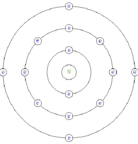
Crystalline silicon is used in the construction of a solar cell. It is a semiconductor material and has some special chemical properties. The silicon atom has 14 electrons which mean it has 4 electrons in the outermost shell. So the silicon atom always seeks to fill the outermost shell. It usually does this by sharing 4 electrons of other atoms to fill up the outermost orbit and form crystalline structure. (Scott 2000)
Figure 2.1 shows the electron configuration of the silicon.
Figure 2.1 Silicon atom configuration
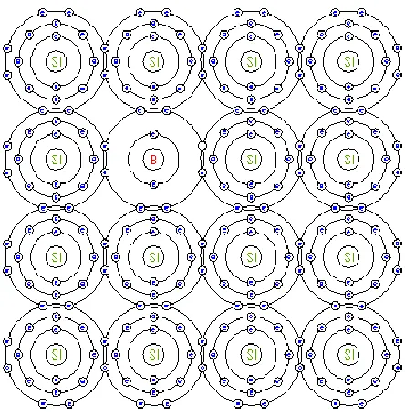
Figure 2.2 Crystalline structure of Silicon
Figure 2.3 P-type Silicon Semiconductor
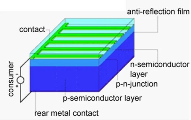
When p-type and n-type semiconductors are joined together, the transfer of electrons and holes takes place at their junction. After some time, they form a “barrier” to resist the further transfer which makes it harder for electron from n-type to transfer to p-type. As this
equilibrium is reached, an electric field is formed at the junction. When a group of photons (solar light) are incident on the cell, they each have sufficient energy to knock off one electron from the junction. If an external path is provided to the junction, then the electrons flow constituting current. In the construction of a solar cell, p-type and n-type
Figure 2.4 Structure of the Solar Cell (Scott 2000)
2.2 Increasing Solar Cell Efficiency
The efficiency of solar cells being used these days is between 14 and 18 Percent. (Markvart & Castaner, 2005) Many researchers are working on increasing this efficiency in order to balance out production costs. Following are some of the approaches they are using in order to achieve this:
1) Different Materials
Different materials like monocrystalline photovoltaic, conductive polymers are being developed. These materials have higher light absorptivity and convert it to electricity more efficiently. (ibid)
2) Different Production Methods
Some of the methods are concentrated on increasing the available surface area of the cell for energy conversion. Chemical etching and texturing of solar cells is done before applying the n-type layer coating. These processes roughen the cell‟s surface introducing uneven areas with peaks and valleys. This increases the available surface area and therefore these cells have better energy conversion rates when the light is incident at different angles. (ibid)
3) Different cell design
The design of the cell can be changed to increase its efficiency. Multi-junction cells, Buried Contact solar cells and Emitter Wrap-Through solar cells are among the different cell designs. (Neuhaus and Munzer,2007)
2.3 IV Characterization of Solar Cell
Solar cells, also known as PV (Photovoltaic) cells, are energy conversion devices. Their performance is measured by estimating the produced power. The performance of the solar cell is determined by plotting current-voltage (I-V) curves. These curves represent the relationship between current and voltage produced in the solar cell. The I-V curves are plotted at constant cell temperature as the exposure of light is maintained at constant level. The current produced by the cell is measured while the resistance of the load is varied. Solar cells can be represented as a current source which is in parallel with a diode. Current is not produced in the absence of light, in which case the solar cell acts as a diode. The current produced by the solar cell depends on both the intensity and wavelength of the incident light. When the incident light intensity is increased, the current produced by solar cell is also increased. (National Instruments, 2009)
While plotting I-V curves for the solar cell, the voltage is represented on the x-axis and the current is represented on the y-axis. It can be seen in the following figure 2.5 that in the absence of light the I-V curve for solar cell is the same as the I-V curve plotted for a diode. As the incident light intensity is increased, the I-V curve will shift. (ibid)
A wide range of voltages and currents can be applied to solar cell operation. The load
resistance can be varied from zero (maintaining a short circuit) to infinity (keeping the circuit open) while the current is measured. The point at which maximum power is delivered by the cell can be used to determine the highest efficiency of the solar cell. (ibid)
Let Il be the current produced by the photoelectric effect and ID be the diode current in an ideal cell. The total current I is calculated from the difference between Il and ID.
The equation 2.1 for the total current I is written as,
I = Il –ID = Il – I0( eqV/kT – 1)………...(2.1) Where I0 – Saturation current of the diode
q - Elementary charge 1.6x10⁻¹⁹ Coulombs k - Constant of value 1.38x10⁻²³J/K T - Cell temperature in Kelvin
V - Measured cell voltage which is either produced or applied (ibid) The above equation 2.1 can be expanded to,
I = Il – I0( exp[q(V+I.Rs)/n.k.T] -1) – (V+I.Rs)/Rsh………..(2.2) Where Rs – Series resistance
Rsh – Shunt resistance
The equivalent circuit of the solar cell can be shown in figure2.6
Figure 2.6 Equivalent circuit for the solar cell (National Instruments, 2009)
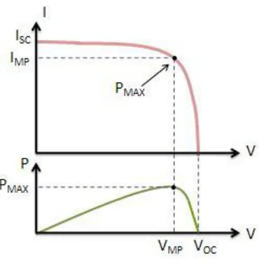
The load resistance is varied from zero to infinity and the I-V graph is plotted. The I-V curve is shown in figure 2.7. ISC represents the short circuit current and VOC represents the open circuit voltage.(ibid)
2.3.1 Short Circuit Current (ISC)
The short circuit current corresponds to the condition when both the positive and negative terminals of the cell are short circuited and the voltage is zero. The load resistance remains zero (ibid).
ISC has the maximum current value in the power quadrant. For an ideal cell ISC is the total current produced the photoelectric effect (ibid).
ISC = IMAX = Il for forward bias quadrant ……….(2.3)
2.3.2 Open Circuit Voltage (VOC)
The open circuit voltage corresponds to the condition when both the positive and negative terminals of the cell are open and the current is zero. The load resistance has infinite value (ibid).
VOC has the maximum voltage difference value in the power quadrant (ibid).
VOC = VMAX for forward bias quadrant……….(2.4)
2.3.3 Maximum Power ( PMAX)
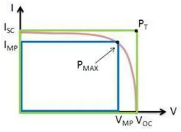
Figure 2.8 Maximum power for IV curve of solar cell (National Instruments, 2009) Figure 2.8 shows the maximum power for IV curve of the solar cell. IMP and VMP are current and voltage at the maximum power point respectively. The maximum power point represents the maximum efficiency of solar cell for conversion of light energy into electrical energy. (ibid)
2.3.4 Fill Factor (FF)
This parameter measures the squareness of I-V curve. It is the measure of quality of a solar cell. The Fill Factor can be calculated by comparing maximum power (PMAX) to the
theoretical power (PT). Theoretical power can be assumed as power output at short circuit current and open circuit voltage. (ibid)
Figure 2.9 Fill Factor (National Instruments, 2009)
Figure 2.9 shows the fill factor for the solar cell. The larger fill factor is desired as it
approaches to the squareness of IV curve. Fill Factor is represented in percentage. Typically values of fill factors are between 0.5 and 0.82. (ibid)
2.3.5 Efficiency (η)
Efficiency of the solar cell is defined as the percentage of light energy incident on solar cell which is converted in to electrical energy. It is the ratio of output power of the solar cell to the input power of the incident light.
η = Pout / Pin ………(2.6)
At the maximum power point, the solar cell operates at maximum efficiency.
ηMAX= PMAX / Pin ………...(2.7) The input power by incident light energy can be calculated as the product of the light
2.3.6 Shunt Resistance (RSH) and Series resistance (RS)
The efficiency of the cell is decreased due to the loss of power across internal resistances. These resistances are represented as shunt resistances and series resistances in the equivalent circuit diagram of the solar cell. (ibid)
In an ideal situation, it is desired that the value of shunt resistance is infinite and the series resistance should have zero value. If the shunt resistance has infinite value, it will not provide an alternate path for current and if the series resistance has zero value, there will not be any voltage drop before the load. (ibid)
Figure 2.10 Effect of series and shunt resistances on IV curve (National Instruments, 2009)
2.4 Manufacturing of solar cell
The manufacturing process of solar cell is expensive and consumes significant energy. As the cell fabrication and module assembly accounts for 25 to 30 percent of the final module cost, the focus of industry has always been to reduce the cost of the manufacturing process of the solar cell.
2.4.1 Silicon Ingots
Most common solar cells are made up of silicon. Silicon is the second most abundant element available on earth. Silicon is obtained from sand in an electric arc furnace as the carbon reacts with silicon dioxide to produce molten silicon and carbon dioxide. The silicon
produced by this process has 1% impurities which is still higher as the semiconductor-grade silicon needs to be hyper pure. These impurities are eliminated by choosing good raw materials, better process and quality control. To achieve electrical properties of
semiconductor, small percentage of dopant atoms are added to pure silicon.(Komp,2002) The electrical current carriers are trapped between the boundaries of the crystals in silicon. This decreases the performance of the semiconductor devices so single crystals of silicon are preferred for fabrication of these devices. Czochralski process is developed to grow silicon crystals. This process can produce single crystal silicon ingots which are six inches in diameter and six feet in length. In this process, seed crystal is dipped into crucible of molten silicon and the crystal is withdrawn slowly. As the seed crystal is pulled the molten silicon at the bottom of the crystal solidifies forming a large round single crystal. Depending upon the size of the crystal to be produced, pulling speed of the seed crystal is adjusted and the temperature of the melt is maintained. The size of the pulling machine and the capacity of crucible to hold the molten material determine the mass and the size of single crystal produced. (ibid)
2.4.2 Creating Wafers
Normally the silicon wafer used in solar modules has thickness of 300 microns. These wafers are cut from single crystal ingot using single-thin metal blade coated with diamonds. In most of the cases the wafering or slicing of silicon ingot is done by washer-shaped blade. The cutting edge of the blade is the inner edge of the blade and the outer edge of the blade is rigidly supported in the heavy ring. During the slicing of the ingot, the lubricant is
continuously pumped in to the saw cut as it cools the ingot and washes away the saw dust. As thousand of wafers can be sliced from one silicon ingot, the process of slicing becomes time-consuming. There is too much material waste involved in the process as half of material is wasted in the form of sawdust. (ibid)
2.4.3 Wafer Polishing and Etching
Solar cells surface should be processed to ensure good electrical and optical properties. Polishing of solar cells is done by using fine abrasives and chemicals. The solar cell surface becomes mirror-like after polishing, this reflective surface provides good junction with the metals which are used as electrical contacts. As the surface reflects significant amount of light, it needs to be textured to increase the absorption of the light by solar cell. Texturing of solar cell surface is done by chemical etching. In this process the surface of the solar cell is etched and the mountain- like structures is made on the surface of the cell. These surfaces are proved to be good absorbent of light as it provides oblique surface to the incident light. (ibid) 2.4.4 P-N Junction
Silicon wafer sliced from the single crystal ingot is p-type semiconductor as the small amount of boron impurity is added to it while forming single crystal. Homogeneous p-n junction is formed by converting top few microns of the wafer into n-type. This is done by incorporating phosphorous atoms at the surface of wafer. The amount of phosphorus added should be more than the boron impurities so that excess of phosphorous being electron donor makes surface of the cell n-type. (ibid)
2.4.5 Antireflection coating
The antireflection coating is applied on the solar cell to ensure maximum absorption of the incident light. Silicon monoxide is coated on the solar cell via vacuum coating process. These coatings are transparent and have thickness less then 0.1 micron. (ibid)
2.4.6 Applying front metal fingers and back contact
Metal contacts are applied by screen printing process on the front and back side of the solar cell. The front metal contacts are made very thin so as to increase the available surface area of the solar cell. The back metal contact is metal coating which reflects back the light through the wafer which is not absorbed. (ibid)
2.4.7 Edge Isolation
2.5 Shunts in the Solar Cell
An alternate path for current is provided by incompletely opened emitter at the edge in the solar cell. There is leakage of current through these paths as these paths provide lower resistances for current flow. (Goetzberger,1998)In solar cell, as the current generated by photons leaks though the shunts it decreases the current generated by solar cell thereby reducing the fill factor (FF) and the open circuit voltage (Voc) . So the presence of shunts in the solar cell decreases its efficiency. (Breitenstein,2004)
Earlier, the term „shunts‟ was used to represent ohmic connection between n and p side of the pn junction. Recent study about shunts shows that shunts show linear IV characteristics as well as non-linear characteristics. As a result shunt can be defined as any local site where the local current exceeds the homogeneously flowing current. This definitions includes shunts due to incompletely opened edge as well as other types of shunts due to material defects. (ibid)
Shunts introduced during the Czochralski process can cause upto 150mA of leakage current.(Langenkamp & Breitenstein,2002)
2.5.1 Linear shunts
The most common type of linear shunt occurs due to incompletely opened emitter at edge. The incompletely opened emitter is the result of improper edge isolation techniques which is carried out during the processing of solar cells to isolate n-type layer and p-type cell
Another kind of linear shunt is formed due to Al particles at the surface. Al particle may be introduced during the stacking of solar cells for drying before firing of the cells. When the firing of the solar cell is done, Al particle alloys on the surface of the cell. These particles creates path between n and p sides of the p-n junction. Sometimes these shunts are also created by laser which cuts through the grid lines alloying the grid particles to the wafer. In the manufacturing of multi-crystalline solar cells, there may be a supersaturation of dissolved carbon in uppermost part of the silicon melts. During the cooling phase the carbon has
tendency to form SiC filaments which grows in large angle grain boundaries. These filaments are highly n- conducting. These filaments introduces low resistance path for the current.(ibid)
2.6 Edge Isolation of Solar Cell
In the manufacturing of Crystalline-silicon solar cell, the p-type silicon semiconductor is diffused with n-type layer (usually Phosphorous). This layer is coated all around the silicon cell. The thickness of this layer is about 15-20 μm. To make the solar cell electrically isolated, the separation between these p-type and n-type layer is required, this isolation is achieved by the edge isolation process where narrow and continuous grooves are scribed through the n-type layer. The width and position of this groove determines the area on the cell available for conversion of the energy. So the width of the groove should be narrow and closer to the edge of the cell to ensure the maximum area. (Colville and Dunsky, 2008) Diamond sawing, Wet-chemical etching and Laser scribing are different methods which are used for edge isolation of solar cell. Diamond saw is used to create the grooves. (Arumughan,
Laser scribing is the widely used process for edge isolation. Direct laser scribing with 1024nm wavelength can introduce micro cracks in the solar cell structure. Depending upon the method used for laser scribing, the process also introduces shunts in the cell structure decreasing its efficiency. (Colville and Dunsky, 2008)
Edge isolation is an important step involved in the manufacturing of the solar cells based on crystalline silicon. During the processing of the solar cell, layer of n-doped silicon is coated around the p-doped silicon wafer. As a result, p-n junction is formed and the electricity is generated across the junction. The layer of the n-doped silicon is very thin having thickness approximately 10-20 μm. The n-doped layer covers the whole area of p-doped wafer
including the edges and surfaces. This creates an unacceptable recombination pathway also known as shunts between the front and back surfaces which prevents the electrical isolation. (ibid)
Figure 2.11 Front view of Solar Cell after Edge Isolation
Figure 2.12 Top view of Solar Cell after Edge Isolation
Edge Isolation Scribe
Width = 25-30 μm Edge Isolation Groove Front Metal Contacts Anti-reflective Layer
Back Metal Contact P-type Semiconductor N-type Layer
3 LITERATURE REVIEW
3.1 Mechanical Edge Isolation
Mechanical edge isolation is the basic technique used for removing edge shunts. The most common mechanical edge isolation techniques are mechanical cutting and laser cutting. Mechanical cutting is done by a dicing saw with diamond dicing blades. Typical thickness of the dicing blade is 0.1 μm. It cuts off the edges of the solar cell during the edge isolation process. Typically material of thickness 1-2 mm is cut from the edges. This method
electrically isolates n-doped front side from the back surface contact. Most of the solar cells used in solar modules have dimensions 125 x 125 mm2. After the edge isolation process the active cell area which is nothing but the n-doped front surfaces is reduced by 3-6%. As the active cell area reduces the short circuit current produced by the cell is also reduced. (Arumughan, et al, 2005)
Similarly, in laser cutting, the laser is used to cut off edges from the solar cell. The
mechanical edge isolation produces significant waste silicon. This waste cannot be recycled. Typically, solar cell has dimensions 125 x 125 x 0.3 mm3. The waste silicon of 174.75g is produced after 500 wafers are processed by mechanical edge isolation. The advantage of this process is that it is an in-line process. (ibid)
Sometimes the edge isolation of the wafer is done by grinding of the edges. This process is easy to carry out as well as setup required is very inexpensive. In this process, a stack containing several cells is processed by sandpaper or industrial beltsander. (Hauser et al, 2001)
3.2 Plasma edge isolation
As the mechanical edge isolation causes reduction in active cell area which reduces the efficiency of the solar cell, plasma edge isolation is preferred over mechanical cutting. Plasma edge isolation has been the standard procedure for edge isolation of solar cell for many years. This process removes silicon from edges but the reduction in the active cell area significantly lowers. For edge isolation of solar cells using plasma etching, the solar cells are stacked together. These solar cells are then put into a vacuum chamber. The etching is done in a fluoride/oxide plasma environment. Typically material of thickness 2-5 μm is removed from the edges as the front n-doped area is electrically isolated from the back contact surface. (Arumughan, et al, 2005)
The coin stacking of wafer provides lower cost/wafer. The main drawback of this method is that it is not in-line process. As the stacking of the wafers is required, the continuous line for production is interrupted. The careful handling of the wafers is required for stacking and to reduce the wafer damages. The higher breakage rates are involved in the plasma edge isolation due to high mechanical force on the wafers at the bottom during the process. (ibid)
3.3 Wet chemical etching
Wet chemical etching process is used for the edge isolation. This process is similar to the plasma edge isolation. The process involves stacking of the wafers and the etching of the edges is carried out by the chemicals like KOH. The chemicals used in the wet chemical etching and plasma edge isolation are hazardous and they need careful handling. Also as stacking of the wafer is required, careful handling of the wafer is required. (Arumughan, et al, 2005), (RENA, 2007)
The main advantage of this process is that the front side of the wafer is not damaged as it does not come in contact with the etching chemical. The stacking of the wafers is eliminated so it minimizes the handling of the wafers and the wafer damages. (ibid)
3.4 Laser scribing
Laser scribing is the most common technique adopted for edge isolation. A thin groove is scribed by laser through the n-doped layer along the edges to achieve the electrical isolation. To achieve the maximum area available for energy conversion, the edge isolation grooves should be narrow and must be close to the edges. Typically groove depth 15-25 μm and width less than 20 μm is needed.
3.4.1 Lasers in Semiconductor Industry
Lasers have unique ability to ablate semiconductor materials with precision as laser processing can achieve resolutions in the range of the laser wavelength.Ultraviolet diode-pumped solid-state lasers are used in scribing of silicon semiconductors in the industry. These lasers provide a focused beam spot with short pulse duration to create extremely high irradiance which can scribe the wafer by instantaneous vaporization. During the scribing of wafer, optimum laser intensity plays an important role. Excessive or insufficient laser
intensity introduces imperfections in the laser scribing process. Optimized laser intensity and highly resolved beam spot are the key requirements to increase the scribing speed of
semiconductor wafer. Optimum laser intensity can be achieved by adjusting laser power, frequency and processing speed whereas high beam spot resolution can be achieved by focusing laser beam to fine spot with the help of optics.(Mendes,2006)
3.4.2 Edge Isolation with Laser MicroJet (LMJ)
Laser MicroJet, manufactured by Synova is water jet-guided laser used for the edge isolation of solar cells. The advantages of this process are high speed and efficient scribing of solar cells with no remnant contamination and avoiding thermal and structural damage to the cell structure. This method can process straight and contour shaped edge isolation grooves as well as cuts.(Synova,2007)
The principal of this technique is incorporating high power pulsed laser beam with a hair-thin low pressure water jet. The laser is coupled to the optical head where focusing lens foucs the laser through quartz window. A chamber filled with low pressure water is connected to the window. Laser focuses into water chamber and the water exits through the nozzle. Total internal reflection at the air/water interface due to differences in the refractive indices leads to the guided laser beam along the cylindrical water jet. The key requirement for this
Nozzle diameter dictates the water pressure at the tip of the nozzle which ranges from 50 bar to 500 bar. Mechanical forces applied by the water jet are very less (0.1N) as compared to the cutting force (1N) for applied by assist gas in laser cutting. This process consumes water at the rate of 1.5 litre/hour.(ibid)
The water jet cools the material between laser pulses which eliminates heat-affected zone problem. The water jet also helps to wash away molten material efficiently from the kerf. To avoid any deposition of particles during process thin water film is maintained on the surface of the wafer. The groove depth of 20 μm is achieved with this process at scribing speed of 250mm/s.(ibid)
3.4.3 Edge Isolation by 20W 1064nm fiber laser
Laser isolation process is carried out by research group at Sungkyunkwan University using 20-watt fiber laser with wavelength of 1064 nm on industrial silison solar cells. The edge isolation is carried out on front as well as back surface. The edge isolation is carried out before and after deposition of SiNx and the results are compared.(Kyeong et al ,2009) During this process edge isolation groove is shifted towards the edge of the solar cell. The groove is scribed 0.2 mm inside the perimeter of solar cell edges on either front side or back side. Laser power pecentages from 20% to 100% in steps of 20% at 100mm/s with repition frequency of 10KHz.(ibid)
3.5 Advantages of the laser edge isolation
1. As laser can be focused at the spot of very small diameter (~10μm). It is possible to create narrow scribes which reduces waste of material.
2. Using higer power laser, processing speed of the edge isolation can be increased.
3. Laser edge isolation facilitates simpler process setup as it is an in-line production process. 4. Mechanical edge isolation process froms debris whereas chemical etching requires haLaser edge isolation is clean aand safer than other edge isolation processes.
3.6 Issues regarding Laser edge isolation
1. The width and depth are not consitant. Depth of the scribe varies when there is inconsitancy.
2. The depth of the scribe is not sufficient to provide high shunt resitances.
We can summerize the different edge isolation techiniques in the following table 3.1. Table 3.1 Comparison of different edge isolation techniques
Edge Isolation
Process Process Technique
Production
Technique Disadvantages
Mechanical Cutting off edges In-Line Waste of material
Chemical/Plasma Etching
Etching away n-type
layer from sides Stacking of wafer
Hazardous Environment
Laser Scribing along the
edges In-line
Higher power induces cracks
4 RESEARCH OBJECTIVES
The research objectives of this thesis are to
To investigate the effect of laser focusing, power and speed on the depth and width of the edge isolation groove.
To understand the internal void formation
To investigate crack-free laser scribing conditions
To formulate a systematic process design mehodology for crack free isolation with suffficient groove width and depth
With respect to above research objectives, the following research approaches are conducted: Study of silicon optical properties
Literature review of crack generation in silicon via laser irradiation. Modeling the laser scribing process
Experimental investigation fo the effects of laser focusing, power and speed. Observing the void formation in CW laser scribing
5 RESEARCH APPROACHES
Based on the above hypothesis, we will first investigate the hypothesized crack formation mechanism during CW laser scribing of Silicon. This investigation is conducted via literature review and experimental validation proposed by (Ohmura et al, 2008). In section 6, a thermal shock phenomenon is applied for the crack generation mechanism. In (Ohmura et al, 2008), a thermal shock model is developed to explain how cracks are achieved in a patented process called stealth dicing, which is used to cut large wafer into smaller pieces.
Based on the results of the stealth dicing we explore the settings for not generating cracks, which is the opposite to the objective of stealth dicing. The selection of such settings is first predicted by a scribing model and then validated by experimental studies. Finally a process design methodology is proposed for selecting optimal setting which produces satisfactory crack-free edge isolation.
5.1 Crack generation mechanism
In the stealth dicing, the crack is created for cutting of silicon wafer. Thermal shock is also generated to propagate crack in the wafer structure. Thermal shock is phenomenon which occurs usually in brittle materials when they are subjected to rapid and extreme temperature fluctuations. This rapid temperature change sometimes results in failure of material by cracking. When brittle materials like glass and ceramics are subjected to rapid temperature fluctuations, thermal gradient is formed in the material. This thermal gradient causes uneven expansion. This uneven expansion causes expansion of molecular bonds in the material and puts stress on the molecular structure of the material. If the thermal gradient is high this expansion of molecular bond overcomes strength of material causes the crack front to advance. (Thermal Shock – Wikipedia)
5.1.1 Void generation by deep focus using pulsed laser
As semiconductor wafers are becoming thinner and thinner it is difficult to dice them using conventional diamond saw. Stresses and mechanical vibrations caused during the dicing by diamond saw create damages in the wafer in form of crack and chipping of the wafer. (Ohmura et al, 2008)
The laser ablation method can be used for successful dicing of the silicon wafer. The laser beam is focused on the surface of the silicon wafer. The wafer surface absorbs the laser energy which causes the ablation of the surface as well as it deforms wafer surface by changing the crystalline structure of silicon. (ibid)
Stealth dicing method is different from other laser material processes. The laser wavelength which can penetrate in the silicon wafer is used for stealth dicing. The laser beam is focused into the silicon wafer. The laser penetrates in the silicon wafer and gets absorbed at the focal point. As the laser is focused into the wafer, there is no damage to the surface of the wafer. This eliminates formation of heat affected zones and the debris pollution which occur in conventional laser dicing method. (ibid)
(Ohmura et al, 2008) studied the stealth dicing method for 50μm silicon wafer. A permeable nanosecond pulse laser is focused inside the silicon wafer. The pulse energy of 4µJ and the pulse width of the half wave height full width value (FEHM) of 150ns were selected during the experiment. The wafer is moved in horizontal direction and the scribe is made. He estimated that the absorption of 1064nm laser when focused in the silicon wafer depends upon the absorption coefficient of the silicon. It is concluded that absorption coefficient increases with increase in the temperature of the silicon wafer. (ibid)
the silicon wafer, crack propagates. (ibid)
Stealth dicing phenomenon is special interest to the edge isolation of the solar cells. Stealth dicing investigates the conditions which causes controlled crack formation in the silicon wafer favorable to the dicing. For successful edge isolation of the silicon wafer the formation of the cracks should be avoided. By examining the conditions in the stealth dicing which do not contribute to the formation of cracks; it is possible to determine parameters for successful edge isolation of the solar cell which is free from cracks.
The most critical process parameter in the stealth dicing is the focus position of the laser. (Ohmura et al, 2008) studied stealth dicing on silicon wafer having thickness 50 μm. The laser was focused on the plane at depths 30 μm, 15 μm and 0 μm. The experiments were carried out at temperature 293K.
5.1.2 Focal plane depth 30 μm
When laser is focused at 30 μm below the surface of the wafer, the laser is absorbed suddenly at depth of 29 μm and the temperature is increased to 12000K instantaneously. The region where the temperature is increased beyond 8000K is vaporized instantly and this leads to formation of the void. There is rapid expansion in the area having temperature beyond 2000K in the surface direction. This generates thermal gradient and the thermal shock wave
Figure 5.1 Top view and cross-sectional view of focal plane at depth 30 μm (Ohmura et al,2008 )
5.1.3 Focal plane depth 15 μm
Figure 5.2 Top view and cross-sectional view of focal plane at depth 15 μm (Ohmura et al,2008 )
5.1.4 Focal plane depth 0 μm
When the laser is focused at the surface, the laser is absorbed suddenly at the surface. This increases the temperature of the surface area. The maximum surface temperature reaches to 60000K. Because of this ultra-high temperature at the surface, violent ablation occurs. The ablation at the surface is no desirable as this generates scattering of the debris and thermal effect. Figure 5.3 shows top view and cross sectional view of focal plane at depth 0 μm. (ibid)
The maximum temperature distributions for above three cases are shown in figure 5.4. When focal plane depth is 30μm, the inside modified layer is generated. Depth of focal plane when changed to 15 μm, the inside modified layer is generates as well as the ablation occurs at the surface. When laser is focused at the surface violent ablation of the surface occurs. (ibid)
Figure 5.4 Temperature distributions for different focal planes (Ohmura et al,2008 )
In stealth dicing method, the laser is absorbed inside the wafer and inside modified layer is formed. The temperature dependence of the absorption coefficient and the thermal wave propagation are reasons for this phenomenon. It is concluded from the results that a suitable focal plane depth should be chosen for stealth dicing so that the thermal shock wave does not reach the surface. (ibid)
For successful edge isolation of the solar cell, the scribe free from cracks is desired. From the above discussion it can be concluded that formation of internal voids should be avoided. As a result, the laser can not be in focused too deep into the substrate. For laser edge
isolation, the condition shown in fig5.4-c should be maintained. For CW laser edge isolation, it is important to explore a scribe as deep as possible before the phenomenon shown in Fig5.4-b.
5.2 Prediction of scribe depth using a heat conduction welding model
The edge isolation scribe is required to have sufficient depth in order to achieve high shunt resistances. The scribe depth varies with change in speed and laser power. Being able to predict the scribe depth is important because the corresponding process parameters can be determined to achieve a particular scribe depth. This can be done through the adaptation of a 2-D heat conduction keyhole laser welding model (Lankalapalli, Tu, et al., 1996). After keyhole welding, the molten material will fill up the keyhole once the surface tension
overcomes the decreased vapor pressure (after the laser beam has passed through), creating a weld. If the power density at the surface is high enough, the vapor pressure inside the
keyhole will increase to a point where it will eject molten material, creating a weld defect called underfill. The power density can be increased by focusing the laser beam near the surface, enhancing this effect and creating a scribe instead of a weld. High assist gas pressure can also be used to help achieve this effect. Therefore, the weld is converted to a scribe. So while this model was intended for predicting the depth of a welding process, it can be used just as effectively to predict the depth achieved in scribing processes.
This model has been previously used to predict welding depths of different materials at higher speeds (Lankalapalli, Tu, et al., 1996 and Paleocrassas and Tu, 2007). Several
Figure 5.5 Keyhole Profile (Lankalapalli, Tu, et al., 1996)
One of the assumptions made, is that the walls of the keyhole within this layer are
Finally, assuming that the thermal properties of the medium are constant and that the axis of the cylindrical surface passes through the origin of the coordinate system, the governing differential equations and boundary conditions for the temperature distribution can be written as: 0 2 2 2 2 x T v y T x T ... (5.1) 2 2 2
at x y a T
T V ... (5.2) y
and as
,y T0 x x
T ... (5.3)
where x and y are the surface coordinates, z is the depth coordinate, a is the keyhole radius, v is the welding speed, is the thermal diffusivity, T0 is the initial temperature and TV is the vaporization temperature of the material (Carslaw and Jaeger, 1962).
After several derivations, the following equation which estimates penetration was found as (Lankalapalli, Tu, et al., 1996)
10 1 0 0 1 1 ( ) ( ) i i V i i P d
k T T c
Pe i
where k is the thermal conductivity of the material and ci are coefficients to a polynomial fit to the equation that was evaluated numerically for 100 different values of Pe in the operating range of 0.0125 - 0.75
3 4 2 3 2 1 2 0 ) , ( )
(Pe G Pe d C C Pe C Pe C Pe
g ... (5.5)
where 1 0 * 0 1 ) cos ( * cos ) ( ) ( ) cos( ) ( * * ) , ( r V V n n n n n Pe T T T T r Pe K Pe K Pe n n Pe I e Pe Pe
G ... (5.6)
where 0 * ) cos * ( 0 ) cos( ) * ( ) ( ) ( * 1 * n n n n n r Pe V
V K Pe r n
Pe K Pe I e T T T T ... (5.7)
Figure 5.6 shows the predicted variation of penetration in Silicon with respect to changes in Péclet number, at different absorbed powers (Pi = 30 – 45 W) for a processing speed range of 75-150 mm/s. Penetration values were calculated using equation 5.4 (see Appendix B for MATLAB model).
Fig.5.6 shows variation of penetration depth with change in Péclet Number. The values on x-axis can be converted into corresponding speeds so that it would be easier to predict
6 EXPERIMENTAL APPARATUS
A 300 W Ytterbium, Single-Mode, Fiber Laser (Figure 6.1) is used for this research. A NEMA two-phase 220V outlet provides electric power to the laser. Its near infrared (1,075 nm) beam is fiber deliverable and comes out of the collimator as a cylindrical 5 mm beam.
Figure 6.1 300 W Ytterbium, single-mode fiber laser power unit
Figure 6.2 Optical isolator connection to collimator, used to divert away reflected laser light into a beam dump
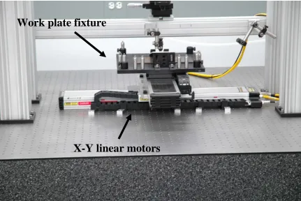
The Parker Automation X-Y linear motors (Figure 6.3) are used to move the workpieces and are controlled by the Galil X-Y axes motion controllers (Figure 6.4). The motors have a resolution of 0.5 μm and a range of 1 m. The maximum acceleration and deceleration is ± 2 g‟s and maximum speed is 1.5 m/s.
Optical isolator
Beam
collimator
Beam dump
Figure 6.3 XY Linear motors with attached work plate fixture
X-Y linear motors
Work plate fixture
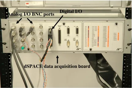
The data acquisition system used is dSPACE 4.0 (Figure 6.5). It is mainly used as an external control for the laser and for acquiring data from sensors (photodiode). This helps automate the operation of the laser. Simulink is used to create different operation schemes and can be synchronized with the movement of the linear motors.
Figure 6.5 dSPACE 4.0 data acquisition system
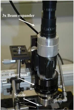
A 3x beam expander is used in combination with the 100.1 mm OptoSigma triplet lens to obtain a minimum focus spot size of 12.01 μm. Equation 6.1 shows how to calculate the minimum spot size.
dSPACE data acquisition
board
Analog I/O BNC ports
Digital I/O
m 12.01 m 9 * 3 * mm 25 mm 1 . 100 Diameter Fiber * Factor Expantion Beam * Length Focal Optics Collimator Length Focal Lens size Spot ... (6.1)
Figure 6.6 Beam expander and laser head setup
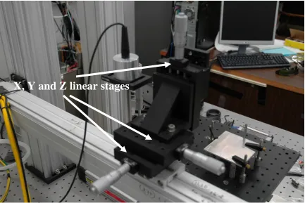
X, Y, Z Linear Micrometer Stages (Figure 6.7) are used to align the optics with the beam. Also, the Z stage is used to change the focusing of the beam, as well as the nozzle height with respect to the workpiece surface. The resolution of the micrometer stages is 10 μm and their range is approximately 26 mm.
3x Beam expander
Laser head
Figure 6.7 X, Y, Z micrometer linear stages
For data acquisition, a Tektronix 3012B oscilloscope was used, shown in Figure 6.8. It has two input channels and the sampling rate capabilities go up to 100 MHz. It always acquires 10,000 samples and the sampling rate is determined by the time range that is chosen.
Figure 6.8 Tektronix 3012B oscilloscope
Figure 6.9 Zeiss Inverted Microscope
7 EXPERIMENTAL PROCEDURES
The experimental procedures to achieve the research objectives are as following Study of silicon optical properties
Modeling the laser scribing process
Experimental investigation fo the effects of laser focusing, power and speed. Observing the void formation in CW laser scribing
7.1 The transmission of LASER through Si Wafer
The experiment is carried out to check the transmission of the LASER through Si wafer. InGaAS photodiode is aligned below the beam expander. The photodiode is fixed on two 75 mm posts. At the start, the laser power is set to 15% power (45W) and the photodiode output is checked. As no output is detected, the laser power is increased by 5% (by 15 W) and the photodiode output is recorded. Laser power is increased in steps of 5% (15 W) and the
photodiode out puts are recorded. Above experiment is carried out placing Si wafer above the photodiode and the outputs are recorded. For each output curve of photodiode, steady state values are calculated. Depending on theese steady state values, the graph is plotted.
7.1.1 100.1 mm lens focusing
The resulting transmission angle is determined using Snell‟s law which is shown in equation 7.1.
nisin i ntsin t……… (7.1) In the above equation, i and t denote the incident side and transmission side of the interface, respectively. From the equation 7.1 transmission angle is calculated from values of the refractive indices and incident angle. Figure (7.1) contains a plot of beam profile with the corresponding change in transmission angle as light passes through silicon. Note: the program used to create Figure (7.1) can be found in the Appendix C.
It is assumed that the laser is focused at the bottom of Si wafer to plot the beam profile. As shown in above figure, ideal spot diameter is ~10μm. However due to refraction of laser into Si wafer spot size increases to ~ 45μm The geometric equations for a Gaussian beam are not exact but they hold as a good approximation.
The beam diameter at different heights can be calculated from following equation.
1/ 2 2 2
0 2
0
4 1 z
M z
d d
d ………..……….(7.2)
Where, a good approximation of d0 is, 2
0
4
L
M f
d
7.2 Controlling parameters for the edge isolation process
The edge isolation process done by the laser is the scribing process. This process can be controlled by adjusting various process parameters which include processing speed, laser power, focus position and assist gas pressure. Experiments were done to examine effect of each process parameter on the edge isolation process. While examining the effect of each process parameter on the process other parameters were kept unchanged. As our aim was to achieve a crack-free edge isolation groove, conditions which contribute to clean groove were observed .An acceptable range of each parameter is determined from the results of these experiments.
7.2.1 Laser Focusing Test
7.2.2 Effect of the focus position on the edge isolation scribe
A 2 cm x 4.5 cm solar cell of thickness 280 μm is selected to perform this experiment. It had soldering material on one side at the bottom. This material was removed by grinding the side of the solar cell by 5 mm using 1200 grit paper on Saphir grinding machine. The solar cell was sandwiched securely between the aluminum fixtures using clamps. The fixture was placed on 75 mm posts and it was fixed using clamps. Flatness of the plate in x-y plane was checked using dial gauge. The clips were adjusted till the flatness of 0.0001” was achieved. The laser power was set to minimum. The minimum power that can be adjusted is 37.5 W with the setup available. Processing speed of 75mm/s was set while performing the
experiment. Initially the focus position of laser was set so that laser is focused on the surface of the solar cell. Four scribes were created for each focus position. After creating each set of scribes, focus position was changed by focusing the laser into the solar cell in intervals of 10 μm. Sample is then observed under inverted microscope to determine geometry of the scribes.
7.2.3Void formation in CW laser scribing
7.2.4 Effect of the power on the edge isolation scribe
A 2 cm x 4.5 cm solar cell of thickness 300 μm is selected to perform this experiment. It had soldering material on one side at the bottom. This material was removed by grinding the side of the solar cell by 5 mm using 1200 grit paper on Saphir grinding machine. The solar cell was sandwiched securely between the aluminum fixtures using clamps. The fixture was placed on 75 mm posts and it was fixed using clamps. Flatness of the plate in x-y plane was checked using dial gauge. The clips were adjusted till the flatness of 0.0001” was achieved. Processing speed of 75mm/s was set while performing the experiment. Focus position for the experiment was selected such that laser is focused just below the surface by 25 µm. Initially 12.5% (37.5W) laser power was selected as it was the minimum power which could be selected with current setup. Two scribes were created for each condition. Power is then increased by 0.5% (1.5W) till it increased to 20% (60W). Sample is then observed under inverted microscope to determine geometry of the scribes.
7.2.5 Effect of the processing speed on the edge isolation scribe
8 RESULTS AND DISCUSSION
Results achived in the experimental procedures are discussed in the following discussions.
8.1 Transmission of the laser through silicon
The table 8.1 shows the values obtained from the experiment of transmission of laser through silicon wafer.
Table 8.1 transmission of laser through silicon wafer.
LASER POWER (W) Photodiode Output Without Si-Wafer (V) Photodiode Output With Si-Wafer (V) Percentage of power transmission
Power at the bottom of the Wafer (W)
45 0.001837653 0.000804677 0.437882995 19.70473479
60 0.002711437 0.000968404 0.357155265 21.42931589
75 0.003596306 0.00114451 0.318246 23.86845002
90 0.004495987 0.001373626 0.305522681 27.49704125
105 0.005431009 0.001536111 0.282840813 29.69828535 120 0.006272782 0.001737432 0.276979496 33.23753958
135 0.0071316 0.001941871 0.272291071 36.75929455
150 0.008011504 0.002133298 0.26627934 39.94190105
Table 8.1 Continued
210 0.01126006 0.002911509 0.258569581 54.29961208 225 0.012038404 0.003057106 0.253946121 57.13787725 240 0.012822843 0.003222715 0.25132609 60.31826171 255 0.013535468 0.003389502 0.250416314 63.85615998 270 0.014225457 0.003545964 0.249268899 67.30260265 285 0.014939221 0.003725655 0.249387502 71.07543794 300 0.015669894 0.003869648 0.246947937 74.08438117
Calibration Curve 0 0.002 0.004 0.006 0.008 0.01 0.012 0.014 0.016 0.018
0 50 100 150 200 250 300 350
Laser Pow er (W)
P h o to d io d e O u tp u t ( V )
Photodiode Output Without Si-Wafer (V) Photodiode Output With Si-Wafer (V)
8.2 Effect of the change in focus position on the scribe
Following are the results obtained from changing the focus position during experiment. The effect on change in width and depth of scribes are examined.
8.2.1 Effect of the focus position on the width of the scribe
Figure 8.2 Effect of the focus position on the width of the scribe on solar cell (pictures)
Effect of the focus position on the width of the scribe
0 5 10 15 20 25 30 35
0 50 100 150 200 250 300
Focus Position ( μm)
W
id
th
(
μ
m
)
Figure 8.3 Effect of the focus position on the width of the scribe on solar cell (graph)
8.2.2 Effect of the focus position on the depth of the scribe
Figure 8.4 The depth of the scribes on solar cell at different focus positions
Effect of the focus position on the depth of the scribe 0 20 40 60 80 100 120
0 50 100 150 200 250 300
Focus Position ( μm)
D e p th (μ m )
Figure 8.5 Effect of the focus position on the depth of the scribe on solar cell Figure 8.5 shows the effect of the focus position on the depth of the scribe.As the laser is focused into the wafer the depth of the scribe increases but it decreases after certain focus position. Although the deeper focus causes deep penetration depths, when penetration depth is much high we get shallower scribes. This is due to the incomplete ejection of melt from the scribe. The mangeta squares in figure 8.5 shows the location of voids due to the incomplete ejection at the bottom of the scribe.
8.2.3 Void formation by deep focus
Figure 8.6 Void formation by deep focus on Si wafer
However, further examination reveals that significant melting occurs in the vicinity of void. Therefor it can be concluded that CW laser and pulsed laser are differrent in their void generation. The void generation of CW scribing is not due to intensive evaporation at the focal point but sililar to porosity during the welding process. This is maninly due to the power deifference between two lasers.
8.3 Effect of the processing speed on the scribe
Following are the results obtained from changing the processing during experiment. The effect on change in width and depth of scribes are examined.
8.3.1 Effect of the processing speed on the width of the scribe
Figure 8.7 Effect of the processing speed on the width of the scribe on the solar cell (pictures)
Effect of the processing speed on the width of the scribe 0 5 10 15 20 25 30 35 40 45
70 80 90 100 110 120 130 140 150 160
Processing Speed( mm/s)
W id th ( μ m )
Figure 8.8 Effect of the processing speed on the width of the scribe on the solar cell (graph)
8.3.2 Effect of the processing speed on the depth of the scribe
Figure 8.9 Effect of the processing speed on the depth of the scribe on solar cell (pictures)
The results of figure 8.9 are surprising. The groove depth becomes shallower similar to the trend predicted by the model. However, as the speed exceeds 100mm/s internal voids appear and the groove depth actually increases. This result is unexpected and needs further
Effect of the processing speed on the depth of the scribe
0 50 100 150 200
70 80 90 100 110 120 130 140 150 160
Processing Speed (mm/s)
D
ept
h
(μm
)
Figure 8.10 Effect of the processing speed on the depth of the scribe on the solar cell (graph)
Figure 8.11Variation of penetration depth of solar cell with change in processing speed
8.4 Effect of the power on the scribe
Following are the results obtained from changing the laser power during experiment. The effect on change in width and depth of scribes are examined.
8.4.1 Effect of the power on the width of the scribe
Figure 8.12 The width of the scribes at different powers on the solar cell (pictures)
Effect of the power on the width of the scribe
20 25 30 35 40 45 50 55 60 65 70
35 40 45 50 55 60 65
Power (W)
W
id
th
(
μ
m
)
Figure 8.13 Effect of power on the width of the scribe on the solar cell (graph)
8.4.2 Effect of the power on the depth of the scribe
Figure 8.14The depth of the scribes at different powers on the solar cell (pictures)
Effect of the power on the depth of the scribe
10 20 30 40 50 60 70 80 90 100
35 40 45 50 55 60 65
Power (W)
D
ept
h
(
μm
)
Figure 8.15 Effect of power on the depth of the scribe on the solar cell (graph)
8.5 Systematic process design methodology
The following design methodology has been formulated:
Step 1 : Based on the scribing model shown in Figure 8.11 choose a combination of power and speed based on the required groove depth.
Setp 2: Conduct focusing test to find the maximum groove depth without internal voids Step 3: Fine tune the speed and power near the initial selection using maximum focal depth according to the scribing model shown in Figure 8.11
Finally based on the results we have found the process conditions of focus 20µm deep, 37.5W power and 95 mm/s speed for the process (Figures 8.16 & 8.17). These parameters produce satisfactory edge isolation groove of depth 62.1 µm without visible evidence of internal voids and cracks.
9 SUMMARY AND CONCLUSIONS
The objectives of the research discuss about the maximum focus position into the material for the crack-free edge isolation. The laser needs to be focused into the material in order to get deeper scribes to increase shunt resistances. The deeper focus position is prone to create void inside the material. This void could act as crack front for crack propagation.
Based on our study, it is true that if we limit the focus position in to the material, there is no formation of void inside the material. However the voids generated by CW and pulsing are quite different.
Theoretical analysis was done to observe reasons for the crack formation in the Si wafer. The deep focus by pulsed laser explained the condition for void formation inside the material. There exists a limit on the focus position for the combination of power and speed. The
estimate on the penetration depth inside the material can be made based on 2-D laser welding model. The focus of the laser changes as it transmits through Si wafer which affect the geometry of scribes generated. The minimum spot size which can be achieved is estimated by studying the beam profile inside the material.