IJIRT 148592
INTERNATIONAL JOURNAL OF INNOVATIVE RESEARCH IN TECHNOLOGY185
Design of Low Power NAND-NOR Content Addressable
Memory (CAM) Using SRAM
Venkatesh Vaidhyam Kannan
1, Rekha CS
2, Deepthi Vijay Kundar
3, Akshatha Arjun Babu Naidu
41,4
MS Student of Electronics Engineering from Kaunas University of Technology (KTU), Lithuania
2Associate Software Engineer in BOSCH, Bengaluru
3Project Engineer in WIPRO, Hyderabad
Abstract-Content addressable memory (CAM) is a type of computer memory used in high speed searching applications. A content addressable memory (CAM) compares input data to the existing stored data in memory and returns the address of the matching data. A CAM usually contains SRAM cell with a comparison circuitry that enables search operations to complete in single clock cycle. In case of advanced applications we need large sized CAM which leads in more power consumption. In order to reduce the power consumed by the CAM cell, the memory circuits used are 6T SRAM and single bit line SRAM as the core storage element. Single bit line SRAM consumes 46.3 percent of power lesser than 6T SRAM.
This paper discusses the implementation of two different architectures of CAM cells namely NAND and NOR type. Power consumption of both architectures are analysed and an efficient NAND-NOR type CAM cell is implemented to overcome its limitations.
Index terms- Bit line, Content addressable memory (CAM), match line, NAND CAM, NAND-NOR architecture, NOR CAM, search line, single bit line SRAM, Static random access memory (SRAM).
I. INTRODUCTION
A Content addressable memory (CAM) cell compares the input data to the stored data in memory and gives the address of the matching data. CAMs work on single clock cycle throughput making them faster than other hardware-and software based search engine. They are used in high speed search applications. In this paper the CAM architecture is implemented in a SRAM cell. [1]
A SRAM cell is memory cell that stores data in 1s and 0s. It consists of different number of CMOS transistors depending on type of SRAM. Conventionally 6T SRAM is used to store the data. But the conventional 6T SRAM consumes more
power, Hence the system performance degrades with the conventional SRAM. So, in order to obtain low power memory cell, different techniques are to be applied and implemented in CAM cell. The time required to find the data stored in memory can be reduced considerably if the data can be identified for access by its content rather than by its address. A memory that is accessed in this way is called content addressable memory or CAM.[2] CAM also provides a performance advantage over other memory search algorithms, such as binary or tree-based searches or look-aside tag buffers, by comparing the desired information against the entire list of pre-stored entries simultaneously, often resulting in the reduction of access time. CAMs are composed of conventional semiconductor memory (usually SRAM) with added comparison circuitry that enables a search operation to complete in a single clock cycle. The two most common search-intensive tasks that use CAMs are packet forwarding and packet classification in Internet routers. In networks like the Internet, a message such as an e-mail or a webpage is transferred by first breaking up the message into small data packets of a few hundred bytes, and then, sending each data packet individually through the network. These packets are routed from the source, through the intermediate nodes of the network called routers, and reassembled at the destination to reproduce the original message. [4]
As CAM applications grow, demand for larger CAM sizes grow, the power problem is further increased. Reducing power consumption, without sacrificing speed or area, is the main thread of recent research in large-capacity CAMs. [5]
IJIRT 148592
INTERNATIONAL JOURNAL OF INNOVATIVE RESEARCH IN TECHNOLOGY186
power dissipation of these 2 architectures in 6T SRAM and single bit line SRAM cells.
II. ARCHITECTURE
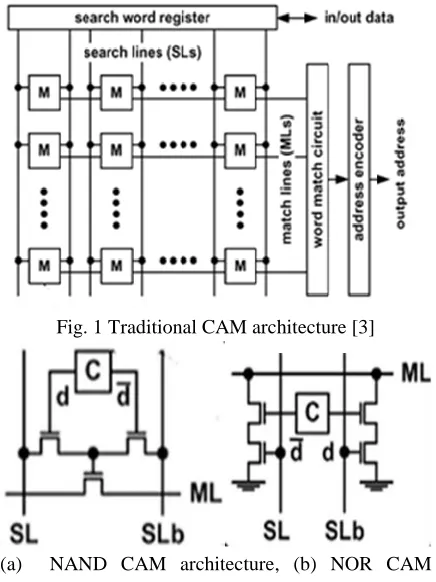
Fig.1. shows CAM architecture which is implemented by storing the data using the memory and the comparison circuit with search line to input the search data. It compares with that of the data stored and the search line input.
Fig. 1 Traditional CAM architecture [3]
(a) NAND CAM architecture, (b) NOR CAM architecture
Fig. 2 Different types of CAM architectures [3] Fig. 2 shows the 2 types of CAM architectures that has been implemented in conventional 6T SRAM and single bit line SRAM.
In comparison with NAND and NOR CAM architectures, NAND consumes less power but has a slower searching speed when compared to NOR CAM architecture that consumes more power. The project mainly includes the implementation of CAM architectures with two different types of memories. The CAM is implemented by storing the data using the memory and the comparison circuit with search line to input the search data. It compares with that of the data stored and the search line input. The implemented architecture is as shown in fig. 2.
Fig. 3 6T CMOS SRAM memory cell As shown in fig. 3, the most commonly used SRAM cell is the full CMOS 6-transistor memory cell. The SRAM cell consists of two inverters and two access MOSFETs which are connected to a pair of bit lines. The gates of two access MOSFETs are also connected to a word line (WL). To form a cross coupled inverter, the output of one inverter is connected to the input of the other inverter and vice-versa. The access transistors enable access to the cell during read and write operations.
Fig. 4 Single bit line SRAM memory cell
As shown in fig. 4, the single bit line SRAM uses 5 transistors with the single bit line. There is a single access transistor with the bit line as the input. The obtained output from the access transistor is fed as the inputs to PMOS and the NMOS transistors to obtain complementary output. The advantage with this SRAM is that there reduction in the dynamic power by 46.3 percent.
III. IMPLEMENTATION
A. NAND type binary CAM cell using 6T SRAM as memory
IJIRT 148592
INTERNATIONAL JOURNAL OF INNOVATIVE RESEARCH IN TECHNOLOGY187
Fig. 5 Schematic for NAND type binary CAM cell using 6T CMOS SRAM
Fig. 5 shows the schematic representation of NAND CAM architecture which uses 6T SRAM as the memory cell. The 6T SRAM is provided with individual pulse voltage sources for bit lines and word line. The output of the memory cell is Q and Q_b. The NAND CAM architecture comprises of 3 transistors in which the source of 2 NMOS transistors are shorted and connected to the gate of the third transistor as shown in the fig. above. The output of the 6T SRAM is fed to the gates of the 2 transistors. The search lines are provided with pulse voltages for their search operation. The output is taken from source of the third NMOS transistor which is connected to a pre-charge circuit. A pre charge circuit is used to keep up with the dropping voltage level at the output. This is in turn connected to an inverter, the output of the inverter is the output of the NAND CAM architecture called as match line.
2) Working of NAND type CAM cell:
The NAND CAM shown above is used to storing and searching for a single bit. The match lines in the CAM cells compare the stored data in the SRAM and search lines. The working of this CAM cell is explained clearly by the table I. The same is represented in the waveform (fig. 6) which is the obtained output at the match lines.
Table I: Outputs for different cases for NAND CAM cell
Fig. 6 Output waveform for NAND type binary CAM cell
B. NOR type binary CAM cell using 6T SRAM as memory
1) Construction of schematic NOR type binary CAM cell:
Fig. 7 Schematic for NOR type binary CAM cell using 6T CMOS SRAM
IJIRT 148592
INTERNATIONAL JOURNAL OF INNOVATIVE RESEARCH IN TECHNOLOGY188
2) Working of NOR type CAM cell:
The NOR CAM cell shown above works in the similar principle to that of NAND CAM cell. The outputs for different cases is as shown in table 1 and the output waveform that is obtained from the match lines is as shown in fig. 6
C. NAND type binary CAM cell using single bit line SRAM as memory
1) Construction of schematic NAND type binary CAM:
Fig. 8 Schematic for implementation of single bit line NAND type binary CAM cell
Fig. 8 shows the schematic representation of NAND CAM architecture which use single bit line SRAM as the memory cell. The single bit line SRAM is provided with individual pulse voltage sources for bit lines and word line. The output of the memory cell are q and q_b. The NAND CAM architecture comprises of 3 transistors in which the source of 2 NMOS transistors are shorted and connected to the gate of the third transistor as shown in the figure 8. The output of the single bit line SRAM is fed to the gates of the 2 transistors. The search lines are provided with pulse voltages for their search operation. The output is taken from source of the third NMOS transistor which is connected to a pre-charge circuit. A pre pre-charge circuit is used to keep up with the dropping voltage level at the output. This is in turn connected to an inverter, the output of the inverter is the output of the NAND CAM architecture called as match.
The power consumed by single bit line SRAM is almost half as that of the conventional 6T SRAM. Thus single bit line SRAM is preferred more over 6T SRAM depending on the power constraints.
2) Working of schematic NAND type binary CAM:
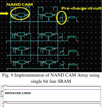
Fig. 9 Implementation of NAND CAM Array using single bit line SRAM
Fig. 10 Output wave form of NAND CAM array The cells in the first row store 0 and 0, the second row store 0 and 1, the third row store 1 and 0, the fourth row store 1 and 1. A common search line is provided for all the 4 columns using individual pulse voltage. The output is taken across the match line which consists of a pre-charge circuit and an inverter. The pre-charge circuit is used to keep up with the dropping voltage levels. In the similar way output is taken for all the 4 rows across the match lines as shown in fig. 9.
Fig. 10 shows the output waveform across match lines for NAND CAM array. When the search data is 0 and 0, match line 1 (i.e. ml-1) goes high indicating that search data is present in first row. Similarly when search data is 0 and 1, match line 2 (i.e. ml-2) goes high indicating that search data is present in second row.
D. NOR type binary CAM cell using single bit line SRAM as memory
IJIRT 148592
INTERNATIONAL JOURNAL OF INNOVATIVE RESEARCH IN TECHNOLOGY189
Fig. 11: Schematic for implementation of single bit line NOR type binary CAM cell
Fig. 12: Implementation of NOR CAM Array using single bit line SRAM
Fig. 13: Output wave form of NOR CAM array Fig. 12 shows the cells in the first row store 0 and 0, the second row store 0 and 1, the third row store 1 and 0, the fourth row store 1 and 1. A common search line is provided for all the 4 columns using individual pulse voltage. The output is taken across the match line which consists of a charge circuit. The pre-charge circuit is used to keep up with the dropping voltage levels. In the similar way output is taken for all the 4 rows across the match lines.
Fig. 13 shows the output waveform across match lines for NOR CAM array, when the search data is 0 and 0, match line 1 (i.e. ml-1) goes high indicating that search data is present in first row. Similarly when search data is 1 and 1, match line 4 (i.e. ml-4) goes high indicating that search data is present in fourth row.
E. NAND-NOR type binary CAM cell using single bit line SRAM as memory
1) Working of NAND-NOR type binary CAM cell:
Fig. 14: Schematic for implementation of single bit line NAND-NOR type binary CAM cell
Fig. 15: Implementation of single bit line NAND-NOR CAM array using single bit line CAM cell. Fig 15 shows 4 X 2 NANDNOR type CAM array which can search 2 bits of data simultaneously. The cells in the first row stores 0 and 0, the second row stores 0 and 1, the third row stores 1 and 0, the fourth row stores 1 and 1. A common search line is provided for all the 4 columns using individual pulse voltage. The output is taken for all the 4 rows across the match lines.
Fig. 16: Output wave form of NAND-NOR CAM array
IJIRT 148592
INTERNATIONAL JOURNAL OF INNOVATIVE RESEARCH IN TECHNOLOGY190
and 0, match line 1 (i.e. ml-1) goes high indicating that search data is present in first row. Similarly when search data is 1 and 1, match line 3 (i.e. ml-4) goes high indicating that search data is present in fourth row.
IV. RESULTS
Using the layout of NAND NOR CAM cells we obtain the RC extraction values for NAND and NOR CAM cell architectures. Layout is created by converting each logic component (cells, macros, gates, transistors) into a geometric representation (specific shapes in multiple layers), which perform the in parasitic extraction is to create an accurate analog model of the circuit. Back Annotation is step to extract parameters such as power, delay by performing post layout simulation.
A. Power consumption
The below table gives a comparison between the power consumed in 6T SRAM and a single bit line SRAM
B. Back annotation
The table below shows the difference in power consumed before and after back annotation and their difference in terms of percentage
V. CONCLUSION
A NAND-NOR based content addressable memory (CAM) has been proposed in this paper in which power consumption is used as the parameter. In the
traditional NOR CAM architecture that uses 6T SRAM memory cell there is a large amount of power consumption, on the other hand in NAND CAM architecture the read and write delays are large but the power consumed is less in comparison to NOR CAM architecture. By the proposed design that is NAND-NOR CAM architecture using single bit line SRAM as memory we observe that there is a significant 16.09% decrease in power consumption compared to NAND-NOR architecture built using 6T SRAM memory. In this paper we have shown the implementation of 4x2 CM array that is 8 bit NAND and NOR CAM architectures for 6T SRAM and single bit line SRAM memories which can search upto 2 bits of data simultaneously.
Thus to overcome the limitations of the traditional NAND and NOR CAM architectures using 6T SRAM as memory cell we propose the NAND-NOR CAM architecture using single bit line SRAM as memory which works on optimum values of power and delay.
REFERENCES
[1] Kostas Pagiamtzis, Student Member, IEEE, and Ali Sheikholeslami, Senior Member, IEEE Content-Addressable Memory (CAM) Circuits and Architectures: A Tutorial and Survey, 2006 [2] S.Vijayalakshmi, B.Elango, V. Nagarajan,
Content Addressable Memory Using XNOR CAM Cell, International Journal of Applied Engineering Research ISSN 0973-4562 Volume 11, Number 1 (2016)
[3] Byung-Do Yang, Yong-Kyu Lee, Si-Woo Sung, Jae-Joong Min, Jae-Mun Oh, and Hyeong-Ju Kang, A Low Power Content IEEE transactions on circuits and systems-I: regular papers, vol. 58, no. 12, December 2011 Addressable Memory Using Low Swing Search Lines
[4] M.M. Soni; P. K. Dakhole FPGA
implementation of content addressable memory based information detection system November 2014