A Charge-Sensing-Capable Source Driver for
TFT Array Testing in System-on-Panel Displays
Chen-Wei Lin and Jiun-Lang Huang
Graduate Institute of Electronics EngineeringDepartment of Electrical Engineering National Taiwan University, Taipei 106, Taiwan
Email: [email protected]
Abstract— Inside a modernflat-panel display, the TFT array acts as the analog memory that stores the image information. To ensure high overall yield, it is crucial to thoroughly test the TFT array before it enters the assembly line. However, TFT array testing gets complicated in system-on-panel displays because the peripheral circuits integrated on the same substrate as the array limit the access to the array’s inputs and outputs. This paper presents a built-in source driver design to facilitate TFT array testbuilt-ing for system-on-panel displays. In addition to writing data to the TFT array pixels, the proposed source driver is capable of executing the charge-sensing test and serial read-out of the charge-sensing results—both help reduce the required test equipment performance and complexity. The proposed source driver has been designed in LTPS technology. Circuit simulation results are shown to validate its performance.
Index Terms— TFT-LCD, TFT array testing, source driver, design-for-test, charge-sensing
I. INTRODUCTION
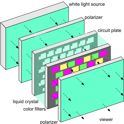
Flat-panel displays have become the market mainstream because they are much lighter and thinner than the tra-ditional CRT (cathode ray tube) displays. In general,flat panel displays have a layered structure. For example, a liquid crystal display (LCD) (Figure 1) is comprised of the light source, polarizers, circuit plate, liquid crystal solution, and color filters. Among them, the circuit plate is responsible for receiving and storing the image infor-mation.
A. TFT array testing
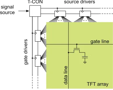
Figure 2 shows the simplified block diagram of a typical LCD circuit plate. It consists of the TFT
(thin-film-transistor) array, the timing controller (T-CON), and the source and gate drivers. T-CON serves two purposes. First, it translates the received image data to a high-speed serial stream, which is the input to the source drivers. Second, it provides the timing and control signals to the source and gate drivers. The TFT array (called array
This paper is based on “A Built-In TFT Array Charge-Sensing Technique for System-on-Panel Displays,” by C.-W. Lin and J.-L. Huang, which appeared in the Proceedings of the 26th IEEE VLSI Test Symposium, San Diego, U.S.A., April 2008. c!2008 IEEE.
This work was partially supported by the National Science Council of Taiwan, R.O.C., under Grant No. NSC 97-2220-E-002-010.
white light source
polarizer
circuit plate
color filters
polarizer liquid crystal
viewer
Figure 1. The TFT-LCD structure.
hereafter for convenience) is basically a two-dimensional pixel cell array. Each pixel cell in general consists of a storage capacitor and a TFT switch. Each time, the gate drivers activate one row of the TFT array by setting the corresponding gate line voltage high; this turns on the pixel switches (see Figure 2 where one pixel is shown) so that the source drivers can write data to the storage capacitors in the selected row.
Array testing characterizes the electrical performance of the two-dimensional pixel array. Its most important goal is to identify and report the nature and location of the defects. (Common TFT array defects include opened or shorted wires [1], [2] and defective pixels [3], [4].) Comprehensive array testing is crucial in yield manage-ment and quality control since it is thefirst opportunity to evaluate the electrical performance of a display and the last reliable opportunity to perform repair on defective pixels and gate/data lines. A defective array that enters the assembly line is a waste of not only the assembly cost but also the other defect-free components.
!"#$% &'()*+,-)./+)&
012+,-)./+)&
!3!,1))14 &.0516
&'()*+
012+,6.5+
-121,6.5+
Figure 2. The circuit plate structure.
array include the voltage imaging scheme, the electron beam scheme [5], and the electrical testing scheme. Al-though the voltage imaging and electron beam schemes are able to inspect all the TFT devices on entire substrate at once, only a few kinds of faults can be detected. Besides, both schemes are limited by the high instrument stability requirement and the long working time. Electrical testing schemes, on the other hand, can perform at-speed testing of the array and evaluate more TFT parameters. Among them, charge sensing is a manufacturing proven approach—it characterizes the array devices as well as locates many types of opened and shorted wires defects. The limitation is that it requires access to all data and gate lines.
Several design-for-test (DfT) techniques have been reported to facilitate electrical testing. In [6], a number of lines are probed as a group and connected “head to tail” in series to form a transmission line. Measuring the resistance of the transmission lines will reveal wire defects. In [7], multiplexers realized with a-Si (amorphous silicon) TFT’s are integrated on the glass so as to reduce the required probe count.
Conventionally, the array is fabricated using the low-temperature poly-Si (LTPS) or a-Si process on glass while the other peripheral and control circuits are fabricated using the popular CMOS technology. Assembly of these components is expensive and error prone. To lower the assembly cost and reduce the display form factor, the trend is to integrate the peripheral circuits and the TFT array on the same substrate (usually glass). Recently, system-on-panel displays with built-in drivers and even the control and timing circuits have been reported [8], [9], [10], [11]. While these highly integrated systems have reduced form factors and enhanced robustness, they pose new challenges to array testing. For example, direct access to the gate and source lines is no longer guaranteed.
B. Contributions
In this paper, we propose to utilize the built-in source drivers to facilitate TFT array charge-sensing testing. To reach this goal, a new source driver design is developed. In addition to writing offset-compensated data to the pixel
!"#$
%&'()*+,-.%
/01123%
32%'%(43+%(3'56
78(8+9'52%
Figure 3. The source driver.
cells, the proposed source driver is capable of performing charge-sensing test as well as serial read-out of the test results. Both the charge-sensing and serial voltage read-out schemes reuse the analog buffers in the source drivers to reduce the area overhead. Moreover, the charge-sensing scheme is able to compensate for the opamp offset voltage due to theVt variations commonly seen in LTPS and
a-Si process. Using the proposed source driver design, the external ATE (automatic test equipment) only needs two analog channels (one to supply the DC reference and the other to sense the serial read-out results) instead of one analog channel for each data line.
The proposed source driver has been designed with LTPS technology and circuit simulation results are shown to validate its performance. The main limitation is the induced area and performance overhead which may be unacceptable for very fine pitch and high refresh rate displays.
C. Paper organization
This paper is organized as follows. In Section II, we will briefly review the offset compensated buffer and the charge-sensing test. The proposed source driver design, the charge-sensing test procedure, and the serial read-out scheme are illustrated in Section III. Finally, circuit sim-ulation results are given in Section IV and we conclude this paper in Section V.
II. PRELIMINARIES
In this section, we will briefly review the source driver, the offset-compensated buffer, and the charge-sensing test.
A. The source driver
!"#$ !
" !
" !%&
! "
!#'
$#'
!"
!#
!#
!$
Figure 4. An offset compensated buffer.
B. The offset-compensated analog buffer
Most TFT arrays are fabricated using the LTPS or a-Si technology. Compared to the mainstream CMOS technol-ogy, LTPS and a-Si TFT devices suffer low mobility and Vt variations [12], [13], [14], [15]. In particular, LTPS
process is prone to spatialVtvariations while a-Si process
is prone to temporalVtvariations.
To compensate for the opamp offset voltage caused by Vtvariations, [15] proposed an offset-compensated analog
buffer design which is shown in Figure 4. The buffer has two operation phases. In the auto-zero phase,φ1 is high
andφ2is low. This way, the offset voltageVOS is stored
in the auto-zero capacitor CAZ. In the functional phase,
φ1 is low andφ2 is high. The buffer outputVD will be
the same as the buffer inputVDAC.
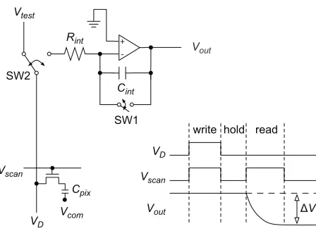
C. The TFT array charge-sensing test
Charge sensing is a common capacitor testing tech-nique [7], [16], [17]. A typical charge-sensing circuit is shown in Figure 5. The charge-sensing procedure consists of three steps: write, hold, and read.
In the write step, SW2 connects the data line to the external test voltage source Vtest and the pixel’s TFT
switch is turned on by bringing Vscan to high. This
way, Vtest is written to the pixel capacitor Cpix. At
this time, the charge-sensing outputVout is initialized by
shorting the opamp’s negative input and output terminals using SW1. In the hold step, Vscan is brought to low to
disconnect the pixel capacitor from the data line. If the pixel is leaky, the pixel voltage will gradually goes down. Finally, in the read step, SW2 connects the data line to the charge detecting circuit. Let Q be the charge stored in the pixel at this time. A voltage drop ∆V =Q/Cint
will be observed at Vout.
In the ideal case, the charge stored in Cpix is Q =
Vtest ·Cpix and we have ∆V = Vtest·Cpix/Cint. In
practice, the pixel is leaky and some of the charge will be lost during the hold period. Let the leakage current be Ileak. The voltage drop becomes
∆V = Vtest·Cpix−Ileak·Thold
CIN T
(1)
whereTholdis the length of the hold duration. Thus, one
can monitor the degree of leakage from∆V.
!
" !
"#$
!$%&$
!'"( )*+$
,*+$
#$% #$&
! -!&'.+
!!
'()*+ ,-./ (+0/
! -!&'.+
!"#$ ,/*0
Figure 5. A simplified charge sensing circuit and its timing diagram.
In addition to monitoring pixel leakage, the charge-sensing test also helps identify opened/shorted wires. For example, if the data line of a column is broken between rown and n+ 1, no voltage drop will be observed for pixels below rown at that column.
III. THEPROPOSEDCHARGE-SENSING-CAPABLE
SOURCEDRIVER
In the proposed source driver, the analog buffer is utilized to facilitate charge-sensing test and serial read-out of test results. In this section, the CS-buffer design will be depicted first. Then, the charge-sensing and serial read-out procedures will be illustrated.
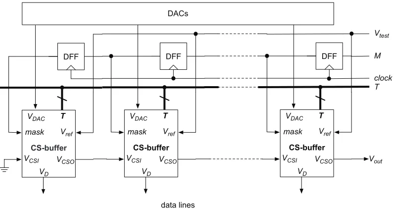
A. The proposed source driver architecture
The proposed source driver architecture is depicted in Figure 6. In this figure, each “CS-buffer” block represents a charge-sensing-capable analog buffer, called CS-buffer in the following discussion. In additional to the functional input from the DAC and the functional output to write the data line, the following I/O’s and circuitry are added to each CS-buffer:
T. T is the control signal bus; it is shared among all the CS-buffers.
Vtest. Vtestis an analog reference signal shared among all
the CS-buffers. Via this port, the external tester supplies the reference voltageVref to each CS-buffer.
M. When performing serial voltage read-out, the CS-buffers are divided into two groups that are configured differently. The mask signal is used to differentiate between these two groups. A D-type flip-flop (DFF) is added to each CS-buffer to store its own copy ofmask value. The DFFs are connected as a shift register and the desiredmaskvalues are delivered to each CS-buffer via the shift operation.
Vout. The Vout port is the analog read-out port where
!"#$%&&'(
!"#$ !"#%
!&'( )*+,
!-." !
!
-!""
!/01
!1'+1
2
34/3, 5
!"#$%&&'(
!"#$ !"#%
!&'( )*+,
!-." !
!
-!""
!"#$%&&'(
!"#$ !"#%
!&'( )*+,
!-." !
!
-!"" !"#$
%&'&()*+,$
Figure 6. The proposed source driver architecture.
VCSI/VCSO. The CS-buffers are concatenated by
con-necting the VCSO port of each CS-buffer to the VCSI
port of the CS-buffer at its right-hand side.VCSO of the
rightmost CS-buffer is then connected to the array’sVout
port.
Control circuitry. Not shown in the figure, the digi-tal control circuitry inside each CS-buffer produces the proper configuration signals according to the shared T and its own masksignals.
The proposed source driver architecture realizes three operation modes: the functional mode, the charge-sensing mode, and the serial read-out mode. In the functional mode, the CS-buffers act the same as the offset compen-sated buffer in Figure 4. In the charge-sensing mode, the CS-buffers perform charge-to-voltage conversion. Finally, the serial read-out mode supports serial readout of the charge-sensing results.
The proposed charge-sensing-capable buffer is shown in Figure 7. Compared to the offset compensated buffer in Figure 4 [15], five more switches are added. Among the switches,φ1 toφ6 facilitate the functional mode and charge-sensing mode operations; the φ7 switch, on the other hand, is activated only during the serial read-out mode.
B. The functional mode operations
Like the offset-compensated buffer in Figure 4, there are two configurations in the functional mode: the auto-zero (AZ) and the write-pixel (WP) configurations. The AZ configuration is shown in Figure 8. (For convenience, only the on-switches are shown.) In this configuration, the opamp offsetVOSis stored in the auto-zero capacitor
CAZ. The WP configuration is shown in Figure 9. Since
the opamp offset voltage has been stored in CAZ, the
buffer output VD will be the same as the buffer’s input,
VDAC.
!"#$ !
" ! "
!%&
!
"
!#'
$#'
!"
!# !$
!%
!()*
!&
!' !(
!)
!$+,
!
$+-Figure 7. The charge-sensing-capable buffer design.
!"#$ !
" ! "
!%&
!
"
!#'
$#'
!"
!#
!$
!%
!&
Figure 8. The auto-zero (AZ) configuration.
!"#$ !
" ! "
!%&
!
"
!#'
$#'
!"
!#
!$
!%
!
" ! "
!"#
!
"
!$%
&$%
!'
!#
!$
!()*
!%
!&
Figure 10. The write data line (WDL) configuration.
C. The charge-sensing mode operations
There are three charge-sensing specific configura-tions: charge-sensing-write-pixel (CWP), write-data-line (WDL), and charge-to-voltage (CTV). A complete charge sensing session involves four configurations in the follow-ing order:
AZ→CWP→WDL→CTV
Note that a pre-defined hold period may be inserted between the CWP and WDL configurations to accentuate the pixel leakage effect.
Charge-sensing-write-pixel (CWP) configuration. This
configuration is the same as the WP configuration except that the CS-buffer input is fromVref rather thanVDAC,
i.e., φ2 is on and φ1 is off. The reason is to gain better
control over the test voltage.
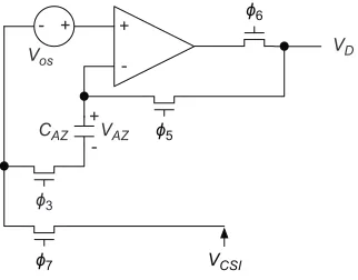
Write-data-line (WDL) configuration. This configuration
is intended to pre-charge the data line to a proper voltage level so that the charge stored in the data line does not affect the measurement results. It should be noticed that the pixel TFT switches must be turned off in this configuration so that the pixel voltages remain intact. The write-data-line configuration is shown in Figure 10. Let the test voltage be Vref = Vbase. The data line will be
written withVbase+VOSand the opamp offset voltage is
stored in CAZ.
Charge-to-voltage (CTV) configuration. In this
config-uration, the stored pixel charge is converted to voltage. The CTV configuration is shown in Figure 11 where the same Vbase as in WDL is applied toVref. Since in this
configuration, the voltage at the negative input of the opamp remains atVbase+VOS which is the same as the
data line voltage, the charge stored in the data line has no effect on the measurement results. Let the pixel voltage at the time of the charge-to-voltage operation beVpix. The
charge-sensing result is:
Vopamp=Vbase
1 +Cpix
CAZ
−(Vpix−VOS)· Cpix
CAZ (2)
where Vopamp is the voltage at the opamp’s output
ter-minal. Define R as the ratio of the pixel capacitance to the auto-zero capacitance, i.e., R =Cpix/CAZ. (2) can
be further simplified as the following.
Vopamp= (1 +R)·Vbase−R·(Vpix−VOS) (3)
! " ! " !"#
! "
!$%
&$%
!'
!#
!()*
!$ !%
Figure 11. The charge-to-voltage (CTV) configuration.
!"#$"
!!
!%&"
" #
" #
" #
!$
!'
!"#$"
!$
!%&"
" #
" # !$
!'
" #
%&'()*"+(),-./&01"2344/5 %&367,"2344/5&01"2344/5
8-9
829
Figure 12. The serial voltage read-out scheme.
In (3), there are two unknowns:RandVOS. A calibration
procedure (described later) is applied to derive or cancel out these two terms. Note that one can add a DC offset toVD by adjustingVbase.
D. The serial read-out mode operations
After the pixel charge has been converted to DC voltage, the test architecture enters the serial read-out mode to transfer the voltages to the Vout port one by
one.
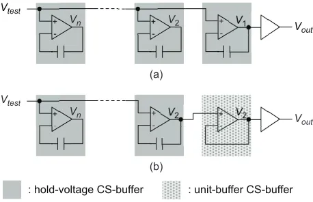
The basic idea of the serial read-out operation is depicted in Figure 12, where each shaded block corre-sponds to one CS-buffer. First, after the charge-to-voltage operation, all CS-buffers are configured to hold the test results at their output terminals, as shown in Figure 12a. At this time, the first CS-buffer’s output voltageV1can be
directly read out from theVoutport. Then, to read outV2,
we configure the first CS-buffer as a unit buffer and let its input be from theVCSI terminal (Figure 12b). This way,
V2 is made available at the Vout port for measurement.
Note that offset compensation must be performed to cancel out the opamp offset voltage. Similarly, to read out V3, we configure the first and second CS-buffers as unit
buffers. To summarize, to transfer a CS-buffer’s charge sensing result to Vout, all the CS-buffers between Vout
and itself are configured as unit buffers.
!
" ! "
!"#
!
"
!$%
&$%
!'
!#
!$
!%
!&
!&()
Figure 13. The read-out-auto-zero (RAZ) configuration.
!
" ! " !"#
! "
!$% &$%
!#
!$
!&'( !&')
Figure 14. The unit-buffer (UB) configuration.
signal is used to differentiate between these two groups of CS-buffers. As shown in Figure 6, each CS-buffer has a DFF to store its ownmask value, and the DFFs form a shift register. During the functional and charge-sensing modes, themasksignal is set to zero for all CS-buffers. In the serial read-out mode,M is set to one. This way, a march sequence of 1 will go through the shift register to realize the serial read-out scheme in Figure 12.
Three configurations are needed to realize the serial read-out operation: hold-voltage (HV), read-out-auto-zero (RAZ), and unit-buffer (UB).
Hold-voltage (HV) configuration. This configuration is the same as the CTV configuration in Figure 11 except that φ5 is turned off to disconnect the opamp output terminal from the data line. This way, further leakage in the pixel will not affect the measurement results.
Read-out-auto-zero (RAZ) configuration. As shown in Figure 13, the RAZ configuration is similar to the auto-zero operation except that the input to the opamp’s positive terminal is from theVCSO output of the previous
CS-buffer.
Unit-buffer (UB) configuration. This configuration is shown in Figure 14. If read-out-auto-zero is performed in advance,CAZ will store the opamp’s offset voltageVOS.
Then, the CS-buffer’s VCSO output will be the same as
its VCSI input.
E. The charge-sensing test flow
The complete charge sensing test flow consists of three sensing sessions. The two additional
charge-!"#$%&!" !#$%&'&!"
()*"+%&,%-,#-+ !#$%&'&!&'($.
"%*/&01$ !# . $%,$&,%,,#0-&.
!"#$%&!" !#$%&'&!"
()*"+%&,%-,#-+ !#$%&'&!&'($ 2
"%*/&01$ !#2 $%,$&,%,,#0-&2
!"#$%&!" !#$%&'&!"
)03/
!#$%&'&!&'($.
()*"+%&,%-,#-+
!#4 $%,$&,%,,#0-&4
"%*/&01$
Figure 15. The charge-sensing test flow.
sensing sessions are needed to deriveR and for opamp offset cancellation. The flow is depicted in Figure 15 in which each grey block represents a complete charge-sensing test session, with or without the hold duration.
Let Vx be the test voltage to be written to the pixels.
In the first test session, charge sensing is performed using Vbase1 as the base voltage, i.e., Vref =Vbase1, and the read-out voltage of the pixel of interest is Vr1. In the second test session, charge sensing is performed using Vbase2as the base voltage, and the readout voltage isVr2. The third test session is similar to the first one except that a hold period is inserted between “writeVx” and “charge
sensing.” The read-out voltage isVr3.
From (3), the three voltage read-out results are as follows.
Vr1 = (1 +R)·Vbase1−R(Vpix+VOS) (4)
Vr2 = (1 +R)·Vbase2−R(Vpix+VOS) (5) Vr3 = (1 +R)·Vbase1−RVpix′ +VOS (6)
Vpix in (4) and (5) represents the pixel capacitor voltage
at the time when the first and second charge sensing operations are performed. If the pixel is leakage free or the amount of leakage is negligible, Vpix will be the
same as Vx. Vpix′ in (6) is the pixel voltage when the
third charge sensing is performed. Since there is a hold period between the write and charge-sensing operations, the leakage effect, if present, should be more apparent in V′
pix.
From (4) and (5),R, the ratio of CpixtoCAZ, can be
derived as follows.
R= Vr1−Vr2 Vbase1−Vbase2 −1
TABLE I.
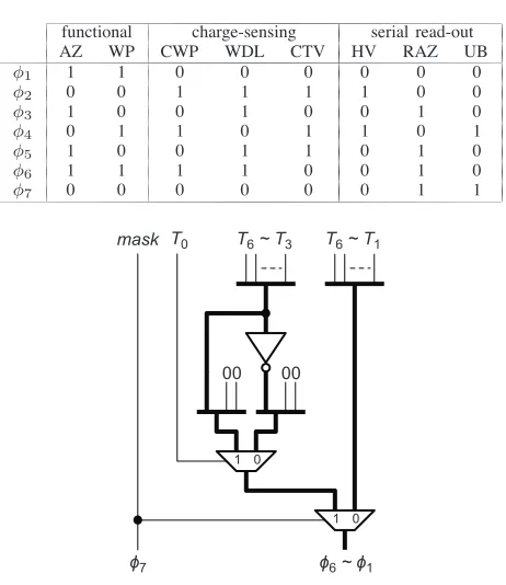
SUMMARY ONCONTROLSIGNALS
functional charge-sensing serial read-out
AZ WP CWP WDL CTV HV RAZ UB
φ1 1 1 0 0 0 0 0 0
φ2 0 0 1 1 1 1 0 0
φ3 1 0 0 1 0 0 1 0
φ4 0 1 1 0 1 1 0 1
φ5 1 0 0 1 1 0 1 0
φ6 1 1 1 1 0 0 1 0
φ7 0 0 0 0 0 0 1 1
!!"#"!" !!"#"!#
$$ $$
$ #
!$
$ #
!!"#"!#
$%&'
!%
Figure 16. Control signal generation.
Then, from (4), (6), and the derivedR, the voltage drop during the hold period can be derived.
∆V =Vpix−Vpix′ =−
Vr1−Vr3
R (8)
The∆V readings allow one to monitor the pixel leakage.
F. Control signal generation
The control signal values with respect to each CS-buffer configuration are summarized in Table I.
One possible implementation of the CS-buffer control logic needed to generate these signals is shown in Fig-ure 16. The T control bus is 7-bit wide, from T6 toT0.
Except for the M signal, the other signals are the same for all CS-buffers.
In this implementation, the φ7 signal is directly
con-nected to the CS-buffer’smasksignal. Whenφ7equals 0,
signalsφ6toφ1are the same asT6toT1. Whenφ7equals
1, the CS-buffer may be in the read-out-auto-zero (RAZ) or the unit-buffer (UB) configuration. The T0 signal is
used to differentiate between these two configurations. If T0equals 1, the CS-buffer is in UB configuration—φ1and
φ2 are set to 0 and φ3 to φ6 are the same as T3 to T6.
If T0 equals 0, the CS-buffer is in RAZ configuration—
φ1 and φ2 are set to 0 and φ3 to φ6 are obtained by
complementingT3 toT6. Note that the T0 signal has no
effect on CS-buffers of which themask signal is 0.
G. Discussions
One circuit implementation issue is the value ofCAZ.
For convenience, let’s rewrite (3) below.
Vopamp= (1 +R)·Vbase−R·(Vpix−VOS) (9)
! "! #! $! %! &! '! (! )!
! " # $ % & ' ( ) * "!
+,-./0102-.3401.5/.2,-.67897:;<=
+,-.->>5>.5/.2,-.5?2@?2.A02,.2,-.01@?2....B
Figure 17. Finite opamp gain effect.
In the right hand side, one can see that the pixel voltage Vpix is amplified by R. If R is too large, Vopamp will
easily become negative and exceed the opamp’s normal operating range. In the following, we chooseR= 1, i.e., CAZ =Cpix. In practice, R will deviate from 1 due to
process variations. Since R will be derived in the post-processing process, the deviation is acceptable if only it does not cause the opamp to malfunction.
In addition to R, the charge-sensing results are also affected by the charge sensing base voltage Vbase. Let
R be unity. To prevent the charge-sensing results from exceeding the opamp’s operating range, the test voltage Vx and the charge-sensing base voltageVbase must meet
the following constraints.
VDD>2·Vbase−Vx+VOS> VSS (10)
The finite opamp gain can lead to measurement errors. The simulation results in Section IV show that when the opamp gain is 20 dB or above, the measurement error is less than 2.5%. If better opamp is used, the error can be further reduced.
IV. SIMULATIONRESULTS
To validate the proposed technique, the CS-buffer is designed using LTPS technology. The simulation setup is as follows. According to [18], CDL andCpix are set to
500 and 700 fF, respectively.CAZ is set to 700 fF so that
R= 1.
A. The finite opamp gain effect
To estimate the impact of finite opamp gain, behavior simulation is performed using an opamp with -1.5 V offset voltage [15]. In Figure 17, the x and y-axes are the opamp gain (dB) and the resulting measurement error (%), respectively. The error is about 2.5% with 20 dB opamp gain, and less than 1% when the gain is more than 25 dB, which is rather easy to achieve in LTPS process.
B. The opamp performance
!"#$%&' () (*)
+%&,-./0'1&2()
34 35 6 5 4 7 8 9 : ; <
+%&,-./'='1&2()'1+>?@!)
34 35 6 5 4 7 8 9 : ; <
A0$BCC/D
!"#$%&'()$*+ !"$,-('
.#/&00-1
2*')(3-"4"5'$+6"52789:6
;< ;= > = < ? @ A B C D
2*')(3-#"5'$+6
;< ;= > = < ? @ A B C D
Figure 18. The unit buffer I/O curve.
! " # $ %
&'()*+,'-.*+&/01.
2 %( !2( !%( "2( "%( #2( #%(
!"! !"# !"$ !"% &
'()*+,-(./+,'012/
3 4) 53) 54) !3) !4) &3) &4)
6789 *
!"#$%&'!#(%)*
!"+,-&'!#(%)*
!" #$ %&'( !" )#$ #(' )*+
Figure 19. The transistor level simulation results.
relation of the unit buffer, obtained via circuit simulation, is shown in Figure 18. Within the target operating range, 0–5 V, the output tracks the input well.
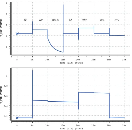
C. Transient simulation results
Transient simulation results of the transistor-level CS-buffer design are shown in Figure 19 where the top and bottom plots correspond to the pixel and the CS-buffer output voltages, respectively. The base voltage is set to be Vbase = 2.5 V and an offset voltage of VOS = 0.35
V is purposely added to the opamp to stress the auto-zero function during the write-data and charge-sensing operations. Also, the pixel is leaky—pixel voltage droop is observed when not driven.
The simulation is divided into 7 phases as marked. The first two phases (AZ and WP) correspond to the functional operations that write 2.5 V to the pixel. In the first AZ, the CS-buffer and pixel outputs are 2.153 V due to the 0.35 V opamp offset. Once the the opamp offset is stored
inCAZ, it is canceled in WP—the pixel voltage becomes
2.494 V which is very close to the ideal value 2.5 V. From the second AZ to the CTV phases correspond to the charge-sensing operation. In the AZ and CWP phases, the offset compensated test data fromVref is written to
the pixel. Then, in WDL, the data line is pre-charged. At the end of WDL, the pixel voltage is 2.642 V. Finally, in CTV, the remaining charge in the pixel is converted to voltage—the simulation result is 1.993 V which is close to the ideal value2·Vbase−Vpix−VOS= 2.008V.
V. CONCLUSION
In this paper, we have presented a built-in source driver design to facilitate TFT array testing. The proposed source driver is capable of executing charge-sensing test as well as serial test results read-out; it helps reduce the ATE performance requirement and the number of analog channels. In the future, we will investigate ways to reduce the induced area and performance overhead due to the CS-buffer.
REFERENCES
[1] Y. M. Liu, M. Miller, F. Henley, M. Nguyen, J. Levine, and H. Steemers, “Line open and short defect classification methodology for AMLCD array test Using voltage imag-ing,”SID Symposium Digest of Technical Papers, 1995. [2] S. L. Wright, K. W. Warren, P. M. Alt, R. R. Horton,
C. Narayan, P. F. Greier, and N. Kodate, “Active Line Repair for Thin-Film-Transistor Liquid Crystal Displays,”
IBM Journal of Research and Development, 1998.
[3] L. C. Jenkins, R. J. Polastre, R. R. Troutman, and R. L. Wisnieff, “Functional Testing of TFT/LCD Arrays,” IBM
Journal of Research and Development, 1992.
[4] Y. C. Lin and H. D. Shieh, “In-Process Functional Testing of Pixel Circuit in AM-OLEDs,” IEEE Transactions on
Electron Devices, 2005.
[5] J. C. Hunter, M. Brunner, R. Schmid, and F. Abboud, “Issues and Challenges Associated with Electrical Testing of Large LCD-TV Arrays,” SID Symposium Digest of
Technical Papers, 2005.
[6] S. L. Wright and R. Nywening, “A Transmission-Line Approach for Line-Continuity Testing of Active-Matrix Arrays,”SID Symposium Digest of Technical Papers, 1995. [7] M. Kodate, F. R. Libsch, T. Iwami, L. Jenkins, M. Mastro, Y. Mekata, R. Polastre, and T. Taguchi, “Next Genera-tion TFT-Array Testing for High ResoluGenera-tion/High Content AMLCDs,” SID Symposium Digest of Technical Papers, 1999.
[8] T. Nagano, H. Kageyama, H. Akimoto, Y. Mikami, and H. Sato, “A 5-Inch SVGA Low-Temperature Poly-Si TFT-LCD with Integrated Digital Interface Driver,” in Inter-national Conference on Solid-State and Integrated-Circuit
Technology, 2001.
[9] T. Nakamura, M. Karube, H. Hayashi, K. Nakamura, N. Tada, H. Fujiwara, J. Tsutsumi, and T. Motai, “Low-Temperature Poly-Si TFT-LCD with an Integrated Analog Circuit,” Journal of the Society for Information Display, 2002.
[10] Y. S. Yoo, J. Y. Choi, H. S. Shim, and O. K. Kwon, “A high accurate analog buffer circuit using low tem-perature poly-Si TFT,”SID Symposium Digest of Technical Papers, 2004.
[11] C. W. Lin, T. K. Chang, C. K. Jan, M. H. Hsieh, C. Y. Tsai, S. C. Chang, and Y. M. Tsai, “LTPS Circuit Integration for System-on-Glass LCDs,” Journal of the Society for
[12] A. Nathan, G. R. Chaji, and S. J. Ashtiani, “Driving Schemes for a-Si and LTPS AMOLED Displays,”Journal of Display Technology, 2005.
[13] S. H. Jung, H. S. Shin, J. H. Lee, and M. K. Han, “An AMOLED Pixel for theVT Compensation of TFT and a p-Type LTPS Shift Register by Employing 1 Phase Clock Signal,”SID Symposium Digest of Technical Papers, 2005. [14] G. R. Chaji, D. Striakhilev, and A. Nathan, “A novel a-Si:H AMOLED Pixel Circuit Based on Short-Term Stress Stability of a-Si:H TFTs,”IEEE Electron Device Letters, 2005.
[15] M.-D. Ker, C.-K. Deng, and J.-L. Huang, “On-Panel Output Buffer with Offset Compensation Technique for Data Driver in LTPS Technology,” Journal of Display Technology, 2006.
[16] A. Laknaur and H. Wang, “Built-In-Self-Testing Tech-niques for Programmable Capacitor Arrays,” in Interna-tional Symposium on Quality of Electronic Design, 2005. [17] S. R. Durbha, A. Laknaur, and H. Wang, “Investigating the Efficiency of Integrator-Based Capacitor Array Testing Techniques,” inVLSI Test Symposium, 2006.
[18] Y. Dai, Design and Operation of TFT Panels. Wu-Nan Culture Enterprise.
Chen-Wei Linreceived his B.S. degree in Electronics Engineer-ing from National Chiao Tung University, Taiwan, in February 2006, after which he received his M.S. degree in Electronics Engineering from National Taiwan University, Taiwan, in July 2007.
Since then he has been working in Thin-Film Transistor Tech-nology Department of Panel integration Division I in Display Technology Center of Industrial Technology Research Institute (ITRI), Taiwan.
Jiun-Lang Huang received the B.S. degree in Electrical En-gineering from National Taiwan University, Taiwan, in 1992, and the M.S. and Ph.D. degrees in Electrical and Computer Engineering from the University of California at Santa Barbara in 1995 and 1999, respectively.