COMPARISON OF CONDITIONAL TECHNIQUES
FOR IMPLICIT AND EXPLICIT
PULSED-TRIGGERED FLIP-FLOPS IN TERMS OF POWER
AND DELAY
Lalita Gupta
1, Mrs. Sangeeta Mangesh
21
M.tech,
2Assistant Professor, Electronics and Communication J.S.S Academy of Technical Education
Noida (India)
ABSTRACT
This paperreviews the three Conditional techniques for high performance flip-flops namely Conditional
Pre-charge, Conditional Capture and Conditional Discharge. The classification of these techniques is based on how
to prevent or reduce the unnecessary internal switching activities and reviewed in terms of Power and
Delay.Comparison summary of flip-flops characteristics based on these techniques are specified and simulation
is carried out. The simulation is carried out by TANNER EDA TOOL using 180 nm CMOS technology, 1.8V
power supply and clock frequency of 250MHz is used for Single edge triggered whereas 150MHz used for
double edge triggered Flip-Flops.
Index Terms: Flip-Flops, Low Power, Pulse Triggered, Digital CMOS.
I. INTRODUCTION
In the earlier, the VLSI designers were bent towards the performance and area of circuits. The power
consumption was a peripheral requirement whereas reliability and cost also gained importance. Recently, power
is being given equal importance in comparison to Speed and area [1]. There are four major components of
power dissipation in digital circuits which are explained by following equation [5].
(1)
(2)
Stands for total power dissipation which constitutes , and currents and switching power
dissipation. The first components represents the switching power dissipation, where α denotes the transition
activity factor and denotes the load capacitance. The is clock frequency. The second component (short
circuit) current which crop-up when both the pMOS and nMOS transistors conduct simultaneously, establishing
a direct current form power supply to the ground. The leakage current, is subjected by two indispensable
sub-threshold current and another component is a reverse diode leakage current. The static current, is
direct current from power supply [1].
In many VLSI chips, the power dissipation of clock system composed of clock interconnection/distribution
consumption. The clock system accounts for 30% to 60% of total power dissipation in a system. As a
consequence, the reduction of power consumption by flip-flops has a deep impact on total power consumption
in a system [2].
Flip-flops and latches are the critical timing elements for storing the information in digital circuits [3]. For the
clock system 90% power is consumed by flip-flops themselves and last branches of clock distribution network
that drives the flip-flop directly. As a clock frequency increases, the latency of flip-flop or latch will play
important role in overall cycle time period. Therefore, to achieve a design that is of high performance of power
efficient, attention must be paid carefully to design of flip-flops and latches [4].
A common flip-flop with lowest power consumption, best performance and maximum robustness against noise
would be an ideal component included in cell libraries. Increasing the performance of flip-flops involve power
and robustness tradeoffs. So, a set of different latches and flip-flops with different performances are necessary to
bind the use of more power consuming and noise sensitive elements only for smaller portion of chips with
performance- critical units.
Timing parameters such as data-to-output latency and setup and hold time are important because the timing
budget is getting close as clock frequency increases. Power requirement is also equally important because of
power consumption increases linearly with clock frequency while the power budget of high performance
portable digital system is limited. In the literature, the comparative analysis of latches and flip-flop commonly
used in high performance system and deal with speed and power trade-offs. The ability to absorb the clock skew
is attaining wide attention to reduce the effect of clock skew that occupies a non-negligible fraction of cycle
time as clock frequency increases. The clock load imposed by flip-flop and latches is important because in high
performance digital system. The power consumption contributed by clock can be as much as 45% of overall
power consumption [6].
In present days, Many modern microprocessors uses master-slave and pulse-triggered flip-flops [2].
Master-slave flip-flops are built by two stages, one master and one Master-slave and they are characterized by their hard edge
property. Examples of master-slave flip-flops are push-pull D-type-flip-flop (DFF) [8], sense amplifier flip-flop
(SAFF) [10],transmission gate based POWERPC 603 [7] and true single phase clocked (TSPC) flip-flops [9].
All these hard-edge flip-flops are characterized by positive set-up time, causing large D-to-Q delays.
Alternatively, pulse-triggered flip-flops reduce two stages into one stage and characterized by soft-edge property
and negative set-up time. The number of stages inside these pulse-triggered flip-flop and logic complexity are
reduced and leading to small D-to-Q delays. One of main advantages of pulse-triggered flip-flops is that they
allow time borrowing across cycle boundaries as a result of zero or even negative set-up time. Due to these
timing issues, pulse triggered flip-flops provide higher performance than master-slave flip-flops.
Depending on the method of pulse generation, pulse-triggered flip-flops can be classified as implicit or explicit
type. In implicit type pulse-triggered flip-flop (ip-FF), the pulse generator is a built-in logic of the latch design,
and no explicit pulse signals are generated [11]. In explicit-type pulse-triggered flip-flop (ep-FF), the pulse is
generated externally and the design of pulse generator and latch are separate.
At first glance, ep-FF consumes more energy due to explicit pulse generator. Explicit-pulse-triggered flip-flop
(ep-FF) and implicit-pulse-triggered flip-flop (ip-FF) have different features. First, ep-FF can have pulse
be more energy efficient than a system using ip-FF. Second, double-edge triggering is straightforward to
implement in ep-FF, but it is difficultin ip-FF. In double-edge triggering, the data latching or sampling is issued
at both the rising and falling edges, usually allow the clock routing network to consume less power. Third,
ep-FF could have advantage of better performance as the height of the nMOS stack in ep-ep-FF is less than that in
FF [2]. With this rationale, ep-FF topology is more suited for low power and high performance designs than
ip-FF.
To obtain the power saving inside the flip-flop, one effective technique can be devised by common property
among the various high-speed flip-flops is the utilization of dynamic structure. This dynamic property causes a
lot of power to be wasted as a consequence of unnecessary internal switching activity, especially in moderate or
low data activity environments. Reducing these activities can effectively result in reducing the overall power
dissipation. Regarding to this, several existing techniques to reduce the internal switching activity are surveyed
and classified into conditional pre-charge, conditional capture and conditional discharge techniques. This paper
reviews these techniques with some associatedflip-flops utilizing these techniques.
II. CONDITIONAL TECHNIQUES
2.1 Conditional Pre-Charge Technique
Fig.1 Conditional Pre-Charge Technique
Fig.1 shows the general scheme of Conditional Pre-chargetechnique. This technique has been applied to low
clock swing flip-flop and save both clock system power and supply power. In this technique, internal node X is
charge that is conditioned by the state of the output. The discharging path is controlled to avoiding the
pre-charging of the internal node X when the input D remains HIGH. When input D goes to high for a long time the
discharge path will be on during the evaluation period causing node X to be dischargeafter each pre-charging
phase in the absence of p-MOS pre-charge control. So, p-MOS is inserted in the pre-charging path to remove the
charging/discharging activities which will prevent the pre-charging of node X in case of input D is stable high.
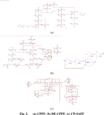
Flip-flops employ this technique such as CPFF [14], DE-CPFF(DE- dual edge) [15] and CP-SAFF (sense
amplifier flip-flop) [16]; they are shown in Fig. 2(a)-(c) respectively. In CPFF and DE-CPFF, the control signal
(a)
(b)
(c)
Fig. 2. (a) CPFF. (b) DE-CPFF. (c) CP-SAFF
2.2 Conditional Capture Technique
Conditional capture technique is presented in [13]. This technique disables unnecessary transition to minimize
the power without effecting speed or no delay penalties. Due to this, it is attractive from point of view of high
performance VLSI implementations. The purpose of Conditional Capture technique is that to derive the internal
nodes significant portion of power is consumed and output remains same. This technique is based on clock
Conditional capture technique is mostly applied for implicit pulse triggered flip flop such as CCFF [12] and
im-CCFF [14] which are shown in Fig. 4(a) and (b), respectively. Flip flops in this technique feature a transparent
window which is used to sample the input. Transparency window, generated by an implicit pulse generator, is
determined by the time when both clocked transistors are on at the same time. The output depend on the input
means output Q will be HIGH when input is HIGH. This output state can be used to close the transparent
window as long as it is HIGH, preventing the unnecessary activities of the internal nodes X.The clock gating in
the conditional capture results in redundant power consumed by the gate controlling the delivery of delayed
clock to the flip flop. As a consequence, Conditional pre-charge technique is better than Conditional Capture
technique in terms of the Energy-Delay-Product (EDP) means it reduces the EDP but the conditional pre-charge
techniquecan only be applied for implicit flip flop.
(a)
(b)
Fig. 4. (a) CCFF and (b) im-CCFF.
2.3 Conditional Discharge Technique
Power saving approach, the clock gating used in Conditional Capture technique results in redundant power
consumed by the gate controlling of delivery of delayed clock to the flip flop but Conditional Pre-charge
technique outperformed the Conditional Capture technique because of reducing in EDP [13] and also
Fig.5 Conditional Discharge Technique
triggering mechanism. So to overcome these limitations, a new technique Conditional Discharge technique has
been used for both implicit as well as explicit pulse triggered flip flop. in this technique, discharge path is
controlled by eliminating the extra switching activity when input is stable HIGH. Fig. 5 shows the idea of
Conditional Discharge technique. CDFF [2] uses a pulse generator which is suitable for the double-edge
sampling. It has two stages. First is responsible for LOW-to-HIGH transition whereas second is responsible for
HIGH-to-LOW transition.
Fig.6 Conditional Discharge Dual-Edge Triggered Flip-Flop,CDFF
An n-MOS transistor controlled by Qb is inserted in the discharge path of the stage with high switching activity.
When input goes to LOW-to-HIGH transition, the output Q changes to HIGH and Qb to LOW. This transition at
the output switches off the discharge path of the first stage to prevent it from discharging when the
input is stable HIGH. CDFF features less switching noise generation which is very important issue in mixed
signal circuits.
III. EXPLICIT PULSE TRIGGERED FLIP FLOP
Pulse triggered flip-flop( Soft –edged) outperform the Master-slave flip-flop (Hard-edged) flip-flop as they
more energy efficient due to explicit pulse generator than ip-FF and do not have any performance advantages
over ip-FF [20]. However, the pulse generator power dissipation overhead distributed among a group of
flip-flops. Moreover, where double-edge triggered flip-flops are considered to reduce the power dissipation of the
clock distribution network [22], the ep-FF is more suitable.
Ep-DCO (explicit pulsed data closed-to- output) flip-flop is the one of the example of ep-FF. it is measured as
one of the fastest flip-flop due to its semi-dynamic nature [20]. Where, to achieve a very small flip-flop delay, it
is well suited for high-performance flip-flop applications. Fig.7 shows the schematic diagram of single-edge
ep-DCO flip-flop; its semi-dynamic structure consists of two stages: first is dynamic and second is static stage. The
pulse generator drives the pre-charge transistor P1 and two evaluation transistor N2 and N3. The N1 serves to
capture the input data when the clock pulse is generated or at the rising edge of the clock, N2 and N3 transistor
are ON for a short time, which equal the delay is created by pulse generator. The flip-flop is transparent and the
input data transfer to tha output. After the transparent period, the pulls down path in both stages are OFF via the
same transistors, N2 and N3. Hence any change at the input cannot be passed to the
Fig.7 Single Edge Triggered Explicit-Pulsed Flip-Flop, ep-DCO
output. There are some disadvantages of ep-DCO flip-flop. There is lot of power consumed at the internal node
X and due to frequent charging and discharging of node in each clock cycle causes glitches to create at the
output. These glitches propagate increase the switching power consumption but also cause the noise problems
that may cause the system out of order.
IV. SIMULATION
Extensive simulation for all flip-flops has been performed in a 180nm CMOS technology at room temperature
using TANNER EDA TOOL. The supply voltage is 1.8 V. The clock frequency of 250 MHz is used for
V. RESULTS AND COMPARISON OF CONDITIONAL TECHNIQUE BASED FLIP-FLOP
CHARACTERISTICS
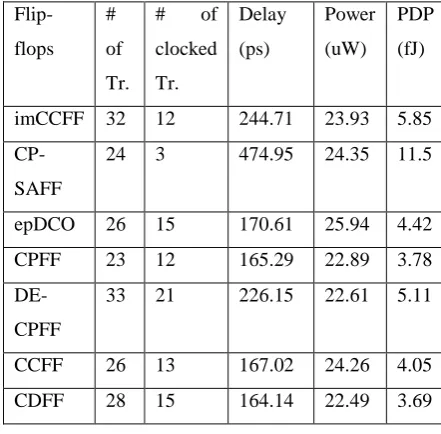
Table1. Shows the simulation results of Conditional technique based flip flops in terms of power, delay and
power-delay-product (PDP). In view of delay, CDFF and ep-DCO have smallest delay because ep-DCO has less
nMOS stack height than CCFF and CPFF; CDFF uses double edge triggering, generally has better driving
ability to help small delay.
Table 1. Comparing the Flip-Flop Characteristics in Terms of Delay, Power and PDP
.
Flip-flops #
of
Tr.
# of
clocked Tr. Delay (ps) Power (uW) PDP (fJ)
imCCFF 32 12 244.71 23.93 5.85
CP-SAFF
24 3 474.95 24.35 11.5
epDCO 26 15 170.61 25.94 4.42
CPFF 23 12 165.29 22.89 3.78
DE-CPFF
33 21 226.15 22.61 5.11
CCFF 26 13 167.02 24.26 4.05
CDFF 28 15 164.14 22.49 3.69
In view of power consumption, CDFF consumes less power while ep-DCO consume more power since
unnecessary switching activity exists at internal nodes.
In view of PDP comparison, CDFF has smallest PDP; CP-SAFF has largest PDP because it has largest delay.
Due to complexity within CCFF and im-CCFF, their PDP are more than CDFF.
VI. CONCLUSION
In this paper, conditional internal activity flip-flops are reviewed and their simulation obtained in terms of
power, delay and PDP. Power optimization and estimation are needed to formulate the low power application
which is required for current and future VLSI design.
REFRENCES
[1] PaanshulDobriyal, Karna Sharma,MananSethi, Geetanjali Sharma "A High Performance D-Flip Flop
Design with Low Power Clocking System using MTCOMS Technique” IEEE International Advance
Computing Conference, 2013.
[2] P. Zhao, T. K. Darwish, and M. A. Bayoumi, “High-Performance and Low-Power Conditional Discharge
Flip-Flop”, IEEE transactions on very large scale integration (VLSI) systems, vol.12 no.5, May 2004.
[3] Saranya. L, Prof. S. Arumugam “Optimization of Power for Sequential Elements in Pulse Triggered
[4] M.-W. Phyu, W.-L. Goh, and K.-S. Yeo, “A low-power static dual edgetriggered flip-flop using an
output-controlled discharge configuration,” in Proc. IEEE Int. Symp. Circuits Syst., May 2005, pp. 2429–2432.
[5] S.M. Kang, Y. Leblebici “CMOS Digital Integrated Circuits analysis and design” third edition, TMH,
2003.
[6] B. Kong, S. Kim, and Y. Jun, “Conditional-capture flip-flop for statistical power reduction,” IEEE J.
Solid-State Circuits, vol. 36, no. 8, pp. 1263–1271, Aug. 2001.
[7] G. Gerosa, “A 2.2W, 80 MHz superscalar RISC microprocessor,” IEEE J. Solid-State Circuits, vol. 29, pp.
1440–1454, 1994.
[8] U. Ko and P. Balsara, “High-performance energy-efficient D-flip-flop circuits,” IEEE Trans. VLSI Syst.,
vol. 8, pp. 94–98, Feb. 2000.
[9] J. Yuan and C. Svensson, “High-speed CMOS circuit technique,” IEEE J. Solid-State Circuits, vol. 24, pp.
62–70, Feb. 1989.
[10] B. Nikolic, V. G. Oklobzija, V. Stojanovic,W. Jia, J. K. Chiu, and M. M. Leung, “Improved
sense-amplifier-based flip-flop: Design and measurements,” IEEE J. Solid-State Circuits, vol. 35, pp. 876–883,
June 2000.
[11] Y.-T. Hwang, J.-F. Lin, and M.-H. Sheu, “Low power pulsetriggered flip-flop design with conditional
pulse enhancement scheme,” IEEE Trans. Very Large Scale Integr. (VLSI) Syst., vol. 20, no. 2, pp. 361–
366, Feb. 2012.
[12] N. Nedovic, M. Aleksic, and V. G. Oklobdzija, “Conditional techniques for small power consumption
flip-flops,” in Proc. 8th IEEE Int. Conf.Electronics, Circuits Systems, Malta, Spain, Sept. 2–5, 2001, pp. 803–
806.
[13] N. Nedovic and V. G. Oklobdzija, “Hybrid latch flip-flop with improved power efficiency,” in Proc.
Symp. Integrated Circuits Systems Design,SBCCI2000, Manaus, Brazil, Sept. 18–22, 2000, pp. 211–215.
[14] N. Nedovic, M. Aleksic, and V. G. Oklobdzija, “Conditional prechargetechniques for power-efficient
dual-edge clocking,” in Proc. Int. Symp.Low-Power Electronics . Design, Monterey, CA, Aug. 12–14,
2002, pp. 56–59.
[15] Y. Zhang, H. Yang, and H. Wang, “Low clock-swing conditional- precharge flip-flop for more than 30%
power reduction,” Electron. Lett., vol. 36, no. 9, pp. 785–786, Apr. 2000.
[16] H. Partovi, R. Burd, U. Salim, F. Weber, L. DiGregorio, and D. Draper, “Flow-through latch and
edge-triggered flip-flop hybrid elements,” in Proc. Dig. ISSCC, Feb. 1996, pp. 138–139.
[17] F. Klass, C. Amir, A. Das, K. Aingaran, C. Truong, R.Wang, A. Mehta, R. Heald, and G. Yee,
“Semi-dynamic and “Semi-dynamic flip-flops with embedded logic,” in Proc. Symp. VLSI Circuits, Dig. Tech. Papers,
June 1998, pp. 108–109.
[18] V. Stojanovic and V. Oklobdzija, “Comparative analysis of master-slave latches and flip-flops for
high-performance and low power system,” IEEE J. Solid-State Circuits, vol. 34, pp. 536–548, Apr. 1999.
[19] J. Tschanz, S. Narendra, Z. P. Chen, S.Borkar, M. Sachdev, and V. De, “Comparative delay and energy of
single edge-triggered & dual edge triggered pulsed flip-flops for high-performance microprocessors,” in
Proc. ISPLED’01, Huntington Beach, CA, Aug. 2001, pp. 207–212.
[20] E. Friedman, “Clock distribution networks in synchronous digital integrated circuits,” Proc. IEEE, vol. 89,