Abstract. We describe and demonstrate a method to deterministically trap single atoms near nanoscale solid-state objects. The trap is formed by the interference of an optical tweezer and its reflection from the nano object, creating a one-dimensional optical lattice where the first lattice site is atz0∼/4 from the
surface. Using a tapered optical fiber as the nanoscopic object, we characterize the loading into different lattice sites by means of the AC-Stark shift induced by a guided fiber mode. We demonstrate a loading efficiency of 94(6)% into the first lattice site, and measure the cooperativity for the emission of the atom into the guided mode of the nanofiber. We show that by tailoring the dimensions of the nanofiber the distance of the trap to the surface can be adjusted. This method is applicable to a large variety of nanostructures and represents a promising starting point for interfacing single atoms with arbitrary nanoscale solid-state systems.
1. INTRODUCTION
The development of hybrid quantum systems is an active field of research [1–3]. Hybrid quantum systems aim to address the conflicting challenges of simultaneous isolation and control of quantum systems by combining two or more systems while preserving their respective advantages. Integrating single atoms with microscopic and nanoscopic objects is of particular interest due to the favorable properties of both systems. On one hand neutral atoms have excellent coherence properties and trapping them close to surfaces is less challenging than with ions [4]. On the other hand nanoscale structures promise strong interactions, scalability and potential applications. The combination of single atoms and nanotechnology allows engineering of strongly interacting systems while maintaining the excellent quantum control of neutral atoms.
To integrate atoms with solid-state systems a crucial challenge is to trap atoms at distances very close to the surface. In particular, in order to realize an efficient atom-photon interface the atom has to be trapped at subwavelength distances from the nanophotonic structure. Trapping at these distances is challenging due to large short-range attractive surface forces (Casimir-Polder and van der Waals) which have to be overcome. Traps for ultra-cold atoms near surfaces have been an active research
ae-mail:
[email protected] bThese authors contributed equally to this work.
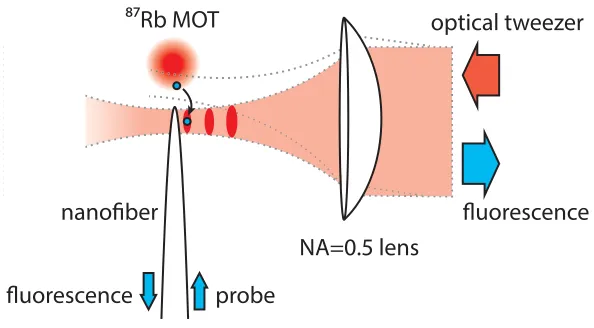
Figure 1. Trapping a single atom near a nanofiber. The trap is formed by the interference of an optical tweezer and the reflection from the nanofiber. The optical tweezer is focused by a high numerical aperture (NA=0.5) lens to a focus with a waist ofw0=0.9m. The one-dimensional optical lattice has a local minimum atz0∼/4 from
the surface of the nanofiber and additional minima spaced by/2. A single87Rb atom is loaded from a MOT at ∼20m from the nanofiber in the optical tweezer and transported into the lattice by scanning the tweezer over the nanofiber. Fluorescence of the atom is collected using single-photon counting modules (SPCMs) through the lens or through the nanofiber. For the measurements in figure3a probe beam is sent through the nanofiber.
topic for many years. Atom-chip [5] methods using magnetic traps generated by patterned electrodes have reached distances down to 500 nm [6,7] using a Bose-Einstein condensate, at which point surface forces [8] become too strong compared to the achievable magnetic trapping forces. Optical dipole traps can be much tighter, and trapping methods based on the steep gradients of evanescent optical fields have been studied extensively [9–11], and have gained interest recently in the context of nanofibers [12–14]. In these experiments a disordered ensemble of atoms is trapped at a distance down to 230 nm from a nanofiber. Optical traps based on lattices induced by reflections from the surface have been demonstrated to confine atoms within 1.5m of a surface [15–17]. Lastly, experiments at distances down to 100 nm have been conducted using untrapped, transiting atoms in the context of surface force measurements [18] and strong-coupling to an optical mode of a microtoroid resonator [19]. To realize an atom-photon interface which is intrinsically scalable a method to deterministically trap single atoms at a subwavelength distance from the surface is required.
Here, we describe and demonstrate a method to deterministically trap single atoms at subwavelength distances from an arbitrary nanoscale object. The trap is formed by the interference of a running wave optical tweezer with its reflection from the nanostructure. The interference pattern creates a trap at a distance of z0∼/4 from the surface (henceforth called the nanotrap), and this distance can be tuned around/4 by tailoring the reflection from the nanostructure. We trap single atoms near a tapered nanofiber and show near perfect loading into the nanotrap. We measure the cooperativity for emission into the guided modes of the single mode nanofiber. Finally, we discuss possible applications of this method.
2. TRAPPING ATOMS NEAR SURFACES
2.1 Trap concept
or loss is crucial for achieving a high loading efficiency and a scalable method for trapping single atoms near nanostructures.
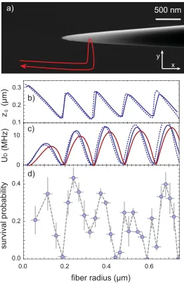
The distancez0of the closest lattice site to the surface is determined by the phase shift of the light scattered from the surface, which for zero phase shift corresponds to z0=/4. Both the amplitude and phase of the reflected field depend on the details of the nanostructure and thereby influence the trap properties. Scattering of a plane wave from a dielectric cylinder is well described in the literature [23,26] and has recently been studied in the context of coupling to the eigenmodes (leaky modes) of nanocylinders [27]. The scattered field is given by a sum over the contributions of the different scattered partial waves which interfere with each other and with the incoming plane wave. This interference modifies both the distance of the trap to the surface as well as the trap depth. Figure2b and2c show the distance to the surface of the nanofiber and the trap depth as a function of fiber radius, calculated both using the analytical solution for a plane wave [23] and a full three-dimensional finite-difference time domain (FDTD) simulation. Both calculations include the Casimir-Polder potential which are obtained using SCUFF-EM [24].
To validate this model we perform a measurement to determine to local trap depth; we trap and cool a single atom as described above and move the atom to a position along the fiber taper axis but offset to the side (as shown in Fig.2a). Subsequently, we load the atom in the optical lattice and transfer it back into free space again where we detect if the atom has survived the trajectory by pulsing on the MOT beams and collecting the atomic fluorescence through the high NA lens as described above. The atom is loaded in a focal plane for which we expect to load either the first or the second lattice site. The first lattice site, however, was likely unstable in this measurement due to rubidium adsorption on the fiber as will be explained below. We repeat this measurement for various positions along the nanofiber axis and measure the survival probability. The results are shown in Figure 2d and show qualitative agreement with the trap depth calculations: the survival probability is proportional to the calculated trap depth. Additionally, from our model we estimate the distance to the surface can be tuned tailoring the scattering phase-shift by±60 nm. This property is a powerful tool to tune the coupling strength of the atom to the nanostructure. The loss of trap depth in such a case can be compensated by using more laser power for the optical tweezer, within the limits of not melting the nanostructure by the highly focussed beam.
To determine the efficiency of loading an atom in the nanotrap we spectroscopically measure a spatially varying AC-Stark shift due to a guided mode in the fiber. This shift is induced by a probe beam sent into the fiber taper and tuned in between the F =1→F=. . . andF =2→F=. . .
Figure 2. a.) A scanning electron microscope (SEM) image of a nanofiber similar to the device used for the presented experiments. The optical tweezer is propagating along ˆzinto the plane. The red line sketches the trajectory of the optical tweezer for loading the nanotrap. b.c.) Simulation of the the distancez0to the fiber surface and the
trap depthUD for a free space trap depthU0=20 MHz as a function of the fiber radius. For an increasing fiber
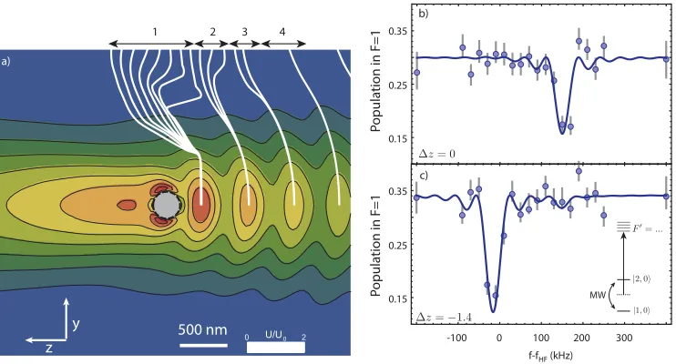
Figure 3. a.) FDTD simulation of the potential in theyz-plane normalized to the free space trap depth; the grey circle is the fiber cross-section. The white lines indicate the local potential minimum for the optical tweezer while it is scanned over the nanofiber. Over a range of focal planes of∼0.8m the trap minimum is translated to the first lattice site. b.-c.) Microwave spectra on the|2, 0 → |1, 0transition probing the spatially-varying AC-Stark shift induced by an off resonant probe beam sent through the fiber. The (higher, lower) frequency peaks show the atoms loaded into the (first, second and higher) lattice sites. The focal plane of the tweezer is in focus with the nanofiber for b. and defocused byz= −1.4m for c. From this data we extract (see text) a loading efficiency of 94(6)% in the lattice of which 100+−012% is in the first lattice site.
by means of optical pumping and coherent transfer. Subsequently, we load the lattice by scanning the tweezer over the nanofiber at a fixed focal plane. Once the lattice is loaded we drive a microwave-pulse to the|F,mF = |1, 0 state and detect the population in theF =1 manifold by heating atoms in the
F =2 manifold out of the trap with resonant light followed by fluorescence detection of the remaining atoms. To load the different lattice sites we modify the focal plane of the dipole trap before loading the lattice. The results are shown in figure3. Accounting for independently measured depolarization due to scattering from the dipole trap and losses from background gas collisions we obtain a loading efficiency of 94(6)% in the lattice of which 100+−012% is in the first lattice site. These results are consistent with lossless loading of the nanotrap. Finally, we measure the lifetime of the atom in the nanotrap to be
=150(20) ms.
The results discussed above show the discrete nature of the optical lattice, however, since accurately determining the absolute power of the probe beam at the fiber tip is challenging and the exponential nature of the confined mode only reveals the relative distance to the fiber surface this measurement is not conclusive for trapping in the lattice site closest to the surface. To determine the absolute distance to the surface we perform an experiment where we drive the atom from the side with a beam resonant with theF =2→F=3 transition. We drive the atom well above saturation, such that (in the limit of weak coupling to the nanostructure) the photon scattering rate is known to be0 =/2, where=
2×6 MHz is the natural linewidth. We collect the photons emitted into the fiber mode with a single photon counting module (SPCM). The ratio of emission into the guided fiber modef versus the free-space emission rate determines the cooperativityC=f/0, which is a strong function of the position
f
f
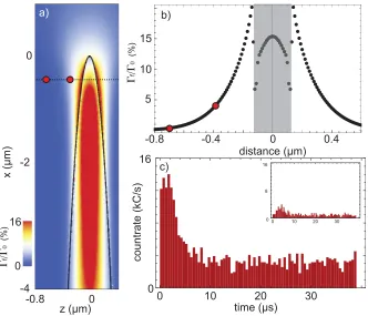
Figure 4. a.) A Boundary Element Method (BEM) simulation of the emission of the atom into the fiber. Plotted is the cooperativity of emitting into the nanofiber mode propagating towards increasing fiber radii and averaged over all atomic dipole orientations. The dashed line shows the x-position where the atom is loaded. The two red circles indicate the position of the calculated trap positions of the first and second lattice site. b.) A cut through the data of figure a. indicated by the dotted line. The shaded gray area indicates the fiber. The two red dots indicate the position of the first and second lattice sites. c.) Photon collection through the nanofiber from an atom loaded in the first lattice site and driven above saturation. Correcting for loss (see text) we determine a cooperativity of
f/0=0.015(6), thereby concluding the atom is trapped in the first lattice site (see text). Inset shows the same
measurement performed for an atom loaded into the second lattice site. The delayed signal agrees with Monte-Carlo simulations of the atom being heated out of the trap and having a finite probability of transiting the fiber after a fews.
the atom is heated out of the trap causing the decay in the fluorescence signal. To obtain the initial position of the atom before scattering photons we analyze the first 250 ns of the fluorescence signal during which the atom cannot have moved by more than 50 nm from the radiation pressure of the probe beam and thermal energy of the atom. For each atom we measure 0.9×10⁻² detector clicks in the first 250 ns. Correcting for quantum efficiency of the detector, atom loss and independently measured fiber coupling efficiency we obtain a cooperativity of C=0.015(6). Here, we have conservatively assumed no loss in the fiber taper, yielding an underestimate for the cooperativity. Comparing this to the numerically calculated cooperativity at the local fiber radius we obtain an upper limit for the distance to the fiber surface of d <375 nm</2, confirming that the atom is trapped in the closest lattice site.
two cases result in significantly different nanotrap polarization: for an optical tweezer propagating along thez-axis and polarized along the nanofiber axis EODT=E0ex, the scattering excites only TM modes
which are also polarized along ex. Therefore, the nanotrap will be linearly polarized. For the case where the optical dipole trap is polarized orthogonal to the nanofiber axis, EODT=E0ey, the scattering excites
TE modes which are polarized in theyz-plane, with a phase and orientation depending on the specific properties of the nanostructure. The interference of the incoming field with the scattered field can result in a strongly elliptical polarized nanotrap. Therefore, the preferred polarization axis for the nanotrap is along thex-axis, which we have implemented in follow-up experiments.
3. CONCLUSION AND OUTLOOK
We have described and experimentally demonstrated a method to deterministically trap and manipulate single atoms at a distance of∼200 nm from a surface. Our results are consistent with lossless loading of the nanotrap and we observe extended lifetimes (>100 ms). We describe how to tune the distance to the surface over±60 nm by tailoring the reflection from the nanostructure. The presented method is largely independent of the nanostructure near which the atom is trapped, therefore, this method is suitable to trap single atoms in the near-field of a large variety of structures. Here, we have demonstrated the method using a nanofiber, and recently we have used this method to trap a single atom in the near-field of a photonic-crystal cavity and observe coupling to the cavity [29].
We acknowledge funding from the NSF, CUA, DARPA, AFOSR, MURI and the Packard Foundation. JDT acknowledges support from the Fannie and John Hertz Foundation and the NSF GRFP. JF acknowledges support from the NSF through a grant to ITAMP.
References
[1] R. J. Schoelkopf, S. M. Girvin, Nature, 451 (2008), 664–669.
[2] M. Wallquist, K. Hammerer, P. Rabl, M. Lukin and P. Zoller, Physica Scripta, 2009 (2009), 014001.
[3] Philipp Treutlein, Claudiu Genes, Klemens Hammerer, Martino Poggio and Peter Rabl, arXiv:1210.4151.
[4] N. Daniilidis, S. Narayanan, S. A. Möller, R. Clark, T. E. Lee, P. J. Leek, A. Wallraff, St. Schulz, F. Schmidt-Kaler and H. Häffner, New J. Phys., 13 (2011), 013032.
[5] J. Reichel, W. Hänsel and T. W. Hänsch, Phys. Rev. Lett., 83 (1999), 3398–3401.
[6] David Hunger, Stephan Camerer, Theodor W. Hänsch, Daniel König, Jörg P. Kotthaus, Jakob Reichel and Philipp Treutlein, Phys. Rev. Lett., 104 (2010), 143002.
[7] Y. Lin, I. Teper, C. Chin and V. Vuleti´c, Phys. Rev. Lett., 92 (2004), 050404.
[8] D. M. Harber, J. M. Obrecht, J. M. McGuirk and E. A. Cornell, Phys. Rev. A, 72 (2005), 033610. [9] Richard J. Cook and Richard K. Hill, Optics Communications, 43 (1982), 258–260.
[10] J. P. Dowling and J. GeaBanacloche, Adv. Atom. Mol. Opt. Phys., 37 (1996), 1–94.
[11] Hammes, M. and Rychtarik, D. and Engeser, B. and Nägerl, H.-C. and Grimm, R., 90 (2003), 173001.
[12] Fam Le Kien, V. I. Balykin and K. Hakuta, Phys. Rev. A, 70 (2004), 063403.
[13] E. Vetsch, D. Reitz, G. Sague, R. Schmidt, S.T. Dawkins and A. Rauschenbeutel, Phys. Rev. Lett., 104 (2010), 203603.
[14] A. Goban, K. S. Choi, D. J. Alton, D. Ding, C. Lacroute, M. Pototschnig, T. Thiele, N. P. Stern and H. J. Kimble, Phys. Rev. Lett., 109 (2012), 033603.
[15] R. A. Cornelussen, A. H. van Amerongen, B. T. Wolschrijn, R. J. C. Spreeuw and H. B. V. van den Heuvell, Eur. Phys. J. D, 21 (2002), 347–351.
[16] J. I. Gillen, W. S. Bakr, A. Peng, P. Unterwaditzer, S. Fölling and M. Greiner, Phys. Rev. A, 80 (2009), 021602.
[17] M. Miranda, A. Nakamoto, Y. Okuyama, A. Noguchi, M. Ueda and M. Kozuma, Phys. Rev. A, 86 (2012), 063615.
[18] V. Sandoghdar, C. I. Sukenik, E. A. Hinds, and Serge Haroche, Phys. Rev. Lett. 68 (1992), 3432– 3435.
[19] Takao Aoki, Barak Dayan, E. Wilcut, W.P. Bowen, A. S. Parkins, T. J. Kippenberg, K. J. Vahala and H. J. Kimble, Nature, 443 (2006), 671–674.
[20] N. Schlosser, G. Reymond, I. Protsenko and P. Grangier, Nature, 411 (2001), 1024–1027. [21] N. Schlosser, G. Reymond and P. Grangier, Phys. Rev. Lett., 89 (2002), 023005.
[22] J. D. Thompson, T. G. Tiecke, A. S. Zibrov, V. Vuleti´c and M. D. Lukin, arXiv:1209.3028. [23] J. R. Wait, Can. J. Phys., 33 (1955), 189–195.
[24] M. T. Homer Reid, http://homerreid.ath.cx/scuff-em/, (2012).
[25] N. P. Stern, D. J. Alton and H. J. Kimble, New J. Phys. 13 (2011), 085004. [26] Lord Rayleigh, Phil. Mag., xii (1881), 81.
[27] Linyou Cao, Justin S. White, Joon-Shik Park, Jon A. Schuller, Bruce M. Clemens and Mark L. Brongersma, Nat. Mater., 8 (2009), 643–647.