Abstract— In this paper dynamic threshold MOS (DTMOS) and its application in a current mirror is discussed. The input/output characteristics of the proposed circuit are discussed. DTMOS technique meets the requirement for the low voltage and low power for the design of analog circuits. Due to larger current driving capacity and low leakage current, DTMOS is attractive for low power applications. In this work high performance super cascode CM is analyzed using DTMOS technique. The designed circuit is simulated using cadence spectre tool and the technology used is 180µm.
Index Terms— CMOS, DTMOS technique, Input resistance, Output resistance, Super cascode configuration, High performances, Low power.
I. INTRODUCTION
The market demand for portable and efficient electronic devices have pushed the industry to design chip with high integration density, low power consumption and better performance .To obtain these objectives the technology size of the CMOS has to face constant downscaling. As the technology is being reduced day by day with the reduction of channel size i.e. Length of the MOSFET, the other parameter dimensions also need to be minimized. Obtaining lower power supplies has become an important aspect in today’s analog and digital circuit design. For existing design methodology in which the design of a low voltage circuit, the power supply must be at least equal to the sum of the magnitude of the cascode p-type and n-type threshold voltage. In the literature several technique such as sub-threshold, self cascade, floating gate, bulk driven, DTMOS, have been proposed to develop a high performance analog circuits under low voltage power supply.
The DTMOS technique in which body (bulk) terminal is connected to the gate terminal is a promising method for achieving enhanced performance without even modifying the existing structure of MOSFET [1].This is the major advantage of DTMOS as it is fully compatible with the conventional CMOS process.
For the existing MOSFET it is necessary to meet the need of Vgs >Vth for the MOSFET to function in the triode or saturation region. In contrast the DTMOS technique allows even smaller voltage to be set at the input terminal and generate saturation voltage at the output terminal [2]. Thus DTMOS technique is applied in the circuit design to get the enhanced performance especially in the low voltage and low power applications. Today DTMOS technique has attracted strong interest from researchers, especially for the design of the building-block circuits such as OTA, Mixer, and Current mirror. In this paper we have applied DTMOS technique in the design of compact current mirror and evaluated the
performance of both the model one with DTMOS technique CM and other without DTMOS technique for 180nm technologies. The paper is organized as follows: the DTMOS technique and its analysis is discussed in section2. Proposed super cascode CM using DTMOS technique is presented in section3. Section4 deals with comparison of measurement and simulation result followed by the wave form using cadence virtuoso tool in 0.8um technology which is followed by the conclusion drawn.
II. BACKGROUND A. DTMOS TECHNIQUE :
The technique behind the dynamic threshold MOS is that the input voltage Vbs is greater than Zero for NMOS and for PMOS it is negative and hence the threshold voltage can be reduced accordingly. The DTMOS structure uses both the gate and the body terminal to provide the signal input. Since in DTMOS both the gate and the body terminal are shorted Vbs become the function of the input signal which is applied to the gate terminal thus Vbs=Vgs is maintained. Due to dynamic body bias, potential in the channel region is strongly controlled by the gate and body terminals, leading to a high transconductance owing to faster current transport. The relation between input signal and VT is described using the following equation
VT0 = 2ɸB + VFB +
2𝑞ɛsNa(2ɸB)
𝐶𝑜𝑥 (1)
Where VFB is the flat band voltage and ɸB is the inversion layer voltage the inversion layer potential, Na is the channel doping, εs is the Si permittivity, q is the electron charge. Considering body biasing, VT is given as
VT = VT0 + γ( 𝛹𝑠 + 𝑉𝐵𝑆 ̶ 𝛹𝑠 ) (2) Where γ = 2𝑞ɛsNa(2ɸB)
𝐶𝑜𝑥 and VT is threshold
voltage due to body effect. The DTMOS transistor and its small signal model is shown in Fig.1.and Fig.2 it has two transconductances, the gate tranconductance (gm) and body transconductance (gmb).And the relation between both the transconductance is given by
Dynamic Threshold MOS (DTMOS)
And its Application
Volume 5, Issue 6, June 2016
Fig.1 DTMOS Transistor
Fig.2 Small Signal Model of DTMOS Transistor
𝑔𝑚 𝑔𝑚𝑏 =
CBC
CGC = 0.2-0.4
Where CBC, CGC are the total body-channel capacitance, the total gate channel capacitance. From Fig.2, the effective input capacitance is given as
CBC =Cgs1 + Cbs1 (3)
From small signal model
Vgs1 = Vbs1 = Vin (4) Applying KCL at the input terminal
Ii =Vin (sCbs1+sCgs1) + (Vin-Vo) (sCbd1+sCgd1) (5) Applying KCL at the output terminal
Io =
𝑉0
𝑟𝑜1 + gmb1Vgs1 + gm1Vgs1 + (Vin-Vo) (sCbd1+sCgd1) (6)
Using value of Vgs from Eq.4 in Eq.6 Io =
𝑉0
𝑟𝑜1 + (gmb1 +gm1) Vin + (Vin-Vo) (sCbd1+sCgd1) (7)
For calculation of unity gain frequency make short circuit current gain = unity i.e. Io (Vo=0) =Ii. Putting Vo = 0 in Eq.5 and Eq.6 and neglecting ro1,
IO = Ii (gmb1 +gm1 - sCbd1 - sCgd1) = (sCbs1+sCgs1 + sCbd1+sCgd1) ɷt = (gmb 1 +gm1) (2𝐶𝑔𝑑 1+2𝐶𝑏𝑑 1+𝐶𝑔𝑠1+𝐶𝑏𝑠1) (8) ft = (gmb 1 +gm1) 2𝛱(2𝐶𝑔𝑑 1+2𝐶𝑏𝑑 1+𝐶𝑔𝑠1+𝐶𝑏𝑠1) (9) Assuming Cgd1=Cgs1=Cdb1=Cbs1=C, gm1=gm,gmb1=gmb in Eq.9 ,we get
ft =
(𝑔𝑚 +𝑔𝑚𝑏 )
12𝛱𝐶 (10)
Since the transconductance of the DTMOS is greater than the conventional CMOS transistor, from equation (10) it is clear that the frequency bandwidth for the DTMOS increases with the increase in the transistor transconductance.
III. PROPOSEDSUPERCASCODECM USINGTHE DTMOSTECHNIQUE
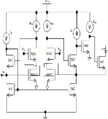
The current mirror shown in fig.3 is a high performance CM, which is the combination of the compact CM structure of Garimell et.al and super-cassode configuration. This CM topology provides very low input-resistance , high output impedance and also has high degree of accuracy,but the supply voltage used is 1.5 V and needs to be improved due to market demands for low voltage, low power devices. In the proposed CM,the conventional supercascode CM is utilized with DTMOS technique.
The DTMOS technique allows the lowering of the supply voltage by reducing the threshold voltage dynamically. Schematic for the proposed CM is shown in fig.4. In the proposed work DTMOS technique is used in the feedback loop of the amplifier A1, A2. In DTMOS technique body of transistor MA11 and MA22 is connected to respective gate of the transistor MA11 and MA22.
Fig.3 (a) Schematic of the conventional super cascode CM
Fig.3 (b) The complete implementation of the super cascode CM
Fig.4 Proposed Modified Design of Super Cascode Structure
This method offers dynamic threshold voltage, which reduces the power consumption of the circuit. Dynamic body bias technique is implemented using triple well CMOS technology which eliminates latch-up and is also compatible with the entire CMOS transistor.
IV. SIMULATIONRESULTANDWAVEFORM
In this section simulation result of the proposed CM have been presented. For the design and simulation of the work cadence virtuoso tool in 0.18μm technology is used. The design parameters for the proposed CM are summarized in Table 1.
Table 1 Design parameters of the proposed CM Component name Value
Technology 1.8μm VDD 1V M1-M5 5μm/0.25 μm M6 20 µm/0.18 μm MA11-MA22 1 µm /0.25 μm IB 10μA IB1 100μA IB2 2μA VB 1.5V iIN 0-500 μA
The super cascode CM and the proposed CM shown in Fig. 3 and 4, is simulated using cadence virtuoso schematic editor and analog design environment. Waveforms for the various parameters are shown below.
Fig. 5 waveform for output current vs input current of supercascode CM
Fig.6 Simulated current matching error ratio of the supercascode CM
Fig. 7 Waveform for power consumption in supercascode CM
Fig.8 Waveform for output current vs. input current of proposed circuit.
Fig.9 Simulated current matching error ratio of proposed CM
Volume 5, Issue 6, June 2016
Fig. 4.6 Waveform for power consumption in proposed CM
All the simulation of the supercascode CM and proposed circuit were done under the similar conditions and same technology for fair comparisons It is observed that using DTMOS technique allows to replicate the input current at the output side with very less offset, it also improves the power consumptions of the circuit. Further going for the ac analysis of the circuit bandwidth of the device also increases by applying DTMOS technique since transconductance of the circuit increases. Transistors always work in the saturation region for analog and RF applications therefore analog and RF characteristics of DTMOS in saturation region are also attractive. The performance of analog circuits strongly depends on how the characteristics of the transistors are exploited and mastered.
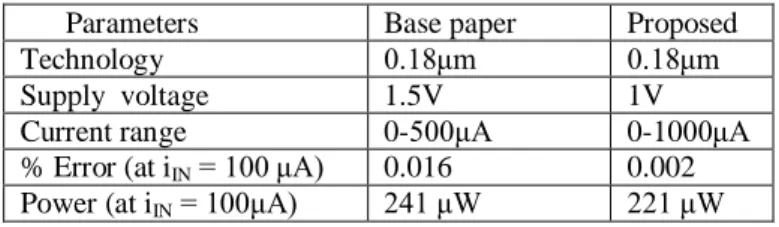
Table 2 Comparative result of super cascode CM and proposed CM
Parameters Base paper Proposed
Technology 0.18μm 0.18μm
Supply voltage 1.5V 1V
Current range 0-500μA 0-1000μA
% Error (at iIN = 100 μA) 0.016 0.002
Power (at iIN = 100μA) 241 μW 221 μW
V. CONCLUSION
In this paper,a modifiefd form of super cascode CM is studied which utilizes DTMOS technique. Modified circuit has high accuracy with very less current copying error. Modified CM consumes less power compared to CM without applying DTMOS technique.
REFERENCES
[1]. E.Sackinger,& Guggenbuhl, W. (1990). “A High-Swing, High Impedance MOS Cascode Circuit”, IEEE
Journal of Solid-State Circuits,Vol .25 No.1,pp 289–298.
[2]. Fariborz Assaderaghi,(1997) Dynamic Threshold-Voltage MOSFET (DTMOS) for Ultra-Low Voltage VLSI IEEE Transactions On Electron Devices, Vol. 44, No. 3,pp.23-28.
[3]. Rajput, S. S., & Jamuar, S. S. (2000). A High Performance Current Mirror For Low Voltage Designs.
IEEE Asia–Pacific conference on circuits and systems (IEEE APCCAS) Vol.23 No.4,pp.270-273
[4]. Xuguang Zhang and Ezz I.El-Mary.(2002), Low-Voltage, Body-Driven CMOS Current Mirror. Dept.
of Electrical & Computer Engineering, Vol.55, No.7,
pp.34-38
[5]. Torralba, A., Carvajal, R. G., Ramirez-Angulo, J., & Munoz, E. (2002), “Output Stage for Low Supply Voltage, High-Performance CMOS Current Mirrors”,
Electronics Letters, Vol.38,No.24,pp.1528–1529.
[6]. Michele Quarantelli, Marco Poles, Marco Pasotti, Pierluigi Rolandi (2003), “High Compliance CMOS Current Source For Low Voltage Applications. VLSI
IEEE Transactions On Electron Devices”, Vol. 132, No.
3,pp.232-238.
[7]. Xuguang Zhang,(2004), “A Regulated Body-Driven CMOS Current Mirror for Low-Voltage Applications”,
IEEE Transactions On Circuits And Systems—II, Vol. 51,
No. 10,pp. 232-236
[8]. Ramirez-Angulo, J., Carvajal, R. G., & Torralba, A. (2004), “Low Supply Voltage High-Performance CMOS Current Mirror With Low Input And Output Voltage Requirements”, IEEE Transactions on Circuits and
Systems II, Vol. 51No.3, pp.124–129.
[9]. Garimella, A., Garimella, L., Ramirez-Angulo, J., Lopez-Martin A. J., & Carvajal, R. G. (2005). “Low-Voltage High Performance Compact All Cascode CMOS Current Mirror”, Electronics Letters, Vol. 41, No.25, pp.1359–1360.
[10]. Koliopoulos, C., & Psychalinos, C. (2007), “A Comparative Study Of The Performance Of The Flipped Voltage Follower Based Low-Voltage Current Mirrors”.
International Symposium on Signals, Circuits and Systems (ISSCS),Vol.67,No.13,pp.745-749
[11]. H.Gabbouj W.Guggenbuhl. (2008), “CMOS Current Mirror For Low Power Applications”, IEEE Journal of
Solid-State Circuits, vol. 89,No.11, pp. 389–398. [12]. Aggarwal, B., & Gupta, M. (2009). “Low-Voltage
Cascode Current Mirror Based On Bulk-driven MOSFET and FGMOS Techniques”, IEEE .International
conference on advances in recent technologies in communication and computing. Vol.56 No.27 pp.
473–477
[13]. Lakkamraju, N., & Mal, A. K. (2011), “A Low Voltage High Output Impedance Bulk Driven Regulated Cascode Current Mirror”, International conference on electronics
computer technology (ICECT) Vol. 3, No.31 pp. 79–83.
[14]. Tikyani, M., Pandey,(2011), “A New Low-Voltage Current Mirror Circuit With Enhanced Bandwidth”, in
Proceedings of the International Conference on
Computational Intelligence and Communication
Networks.Vol.31,No.41, pp. 42–46.
[15]. Gupta, M., Aggarwal, B., & Gupta, A. K. (2013), “A Very
High Performance Self-Biased Cascode Current Mirror For CMOS Technology”, Analog integrated circuits and
signal processing mixed signal letter (Springer),Vol.
75,No.4,pp.67–74.
[16]. N. Raj, A.K. Singh and A.K. Gupta (2014) “Low-Voltage Bulk-Driven Self-Biased Cascade Current Mirror With Bandwidth Enhancement , Electronics Letters, Vol. 50 No. 1 pp. 23–25
[17]. V.Niranjan,A.Kumar, S. B. Jain,(2014), “Maximum Bandwidth Enhancement Of Current Mirror Using Series-Resistor And Dynamic Body Bias Technique”,
Radio engineering, Vol. 23,No.3,pp.321-328.
[18]. Bhawna Aggarwal • Maneesha Gupta •Anil Kumar Gupta (2013) “A very high performance self-biased cascode current mirror for CMOS technology”, Analog Integr Circ
• Sahil Bansal(2014), “A very high performance compact CMOS current mirror”, Analog Integr Circ Sig Process ,Vol.81,No.3,pp.367-375.
Sonam received the B.Tech degree in
Electronics And Communication Engineering from Apeejay college of engineering, Gurgaon in 2012. She is pursuing M.Tech in VLSI Design from Ajay Kumar Garg Engineering College, Ghaziabad. Currently she is working on project named as Dynamic Threshold MOS (DTMOS) and its Applications
Richa Srivastava received the B.E
degree in ECE from Dr. B. R. Ambedkar University, Agra, and M.Tech degree in VLSI Design from Banasthali Vidyapeeth, India in 2003 and 2006 respectively. During 2006-10, she was lecturer in AKGEC, Ghaziabad, India. She has done Ph.D. from NSIT, New Delhi, India. Currently she is working as asst. prof. in AKGEC, Ghaziabad,India. Her research focuses on design of analog integrated circuits for low voltage/low power applications. She has thorough experience on working with various industry-standard VLSI design tools (Tanner EDA; Cadence Virtuoso).