OPTIMISATION OF SPRAY DEPOSITED Sno
2THIN FILM FOR SOLAR
CELL FABRICATION
By
K. Mukhopadhyay, A.J. Varkey
National Centre for Energy Research and Development University of Nigeria, Nsukka
and
C.E. Okeke, H.N. Seyoum
Department of Physics and Astronomy University of Nigeria, Nsukka (Manuscript received December 1986 and in revised form July 1987)
ABSTRACT
The use of conducting tin-oxide (SnO2 ) films for fabrication of solar
cell is becoming increasingly important because of reasonably high efficiency and ease in fabrication. The role of the thin-oxide film is very critical for high efficiency. Resistivity, thickness and transmittance of the film should be of correct order. The most favourable conditions for fabrication of SnO2 layer with low resistivity and high transmittance is
reported in this paper. Effect of doping and annealing on these properties has also been studied. It is observed that doping with antimony gives better layer with sheet resistivity of approximately 60 ohm/square (Ω/◊) and transmittance of the order of 80%. Annealing in air and vacuum shows a decrease in resistivity while it has negligible effect on its transmittance.
Attempts have also been made to fabricate Sn2/Si solar cell with the present
set up, and efforts are being made to optimize its performance.
1. INTRODUCTION
The cost reduction and
simplification of technology
involved in fabrication of solar cells are two major areas where
research efforts are to be
concentrated. Silicon solar cells which are most commonly used are
made up of a single crystal
semiconductor, and junction is
formed using diffusion technique,
which involves sophisticated
technology and high cost.
There exist a number of low cost processes by which simicon Solar cell can be produced. In the last few years SnO2/Si and ITO/Si
solar cells are gaining importance due to its ease in fabrication and
low cost. SnO2 layer could be
deposited in a number of ways, of
which the chemical spraying
technique is rather attractive due
to its simplicity. The salient
feature of the SnO2, is that it only
absorbs in the UV and therefore acts as a window for sunlight [1]. In this device the barrier is located
at the interface and therefore
reduces surface recombination.
The performance of the SnO2/Si
solar cell depends mostly on the proper fabrication of the sn02 layer.
Spraying technique together with suitable doping and annealing, has achieved high conversion efficiency [2-6].
We have successfully set up and used spraying technique for the fabrication of SnO2 /Si solar cell.
Efforts have also been made to optimize conditions that can yield
sn02 layer suitable for cell
fabrication. Effect of doping and annealing is also studied. Finally, the behaviour of SnO2/Si junction is
also reported.
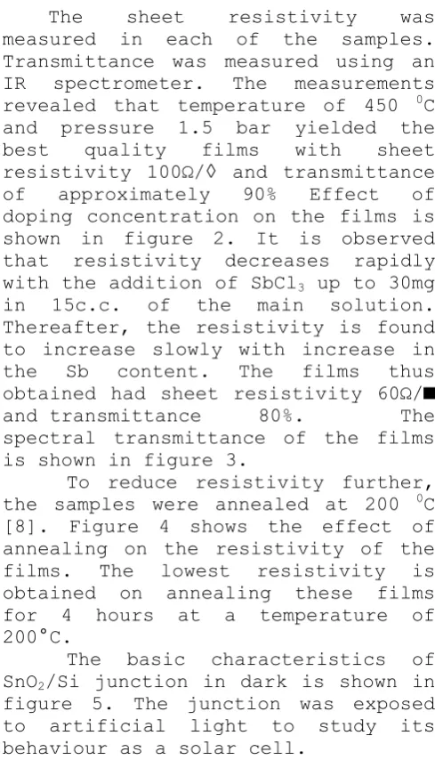
2. EXPERIMENTAL DETAILS
The undoped SnO2 films were
NIJOTECH VOL. 11 NO.1 SEPTEMBER 1987 MUKHOPADHYAY et al 13
required amount of O.lM HCl to keep
the pH value of the solution
approximately 1. Ordinary glass
slide cleaned and etched was used as substrate. The temperature of the substrate was varied between 350C to
5000C keeping it in direct contact
with the heater. The solution was
sprayed onto the substrate at
various temperatures and pressures. Resistivity and transmittance of
each sample were measured to
optimize the temperature and
pressures to obtain good quality
films with reproducible
characteristics. Subsequently. The films were doped with Antimony by adding SbCl3 in the main solution.
Characterization of these doped
films was done as before. This was
repeated for various Sb
concentrations. Effect of annealing
of the films at different
temperatures was also studied to obtain films with low resistivity and high transmittance.
Finally, the films were
deposited on Si substrate to form Sno2 /Si hetero junction. The back
ohmic contact was formed on an n-type Si wafer using electroless technique [7]. One side of the wafer was masked and then dipped into
palladium solution for about 3
minutes at 60-65 0C. It was then
immersed in the electroless nickel solution for 4 minutes. When the back contact was formed, the mask is removed and the front surface is thoroughly cleaned and etched. The
wafer is immediately taken to the spraying chamber for sno2 deposition.
3. RESULTS
The sheet resistivity was
measured in each of the samples. Transmittance was measured using an IR spectrometer. The measurements revealed that temperature of 450 0C
and pressure 1.5 bar yielded the
best quality films with sheet
resistivity 100Ω/◊ and transmittance
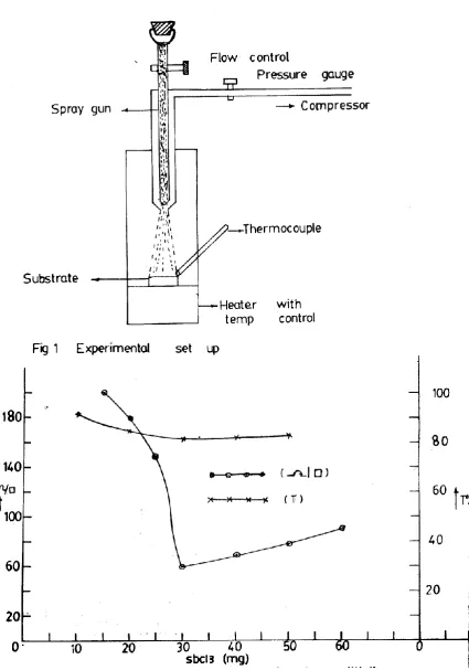
of approximately 90% Effect of
doping concentration on the films is shown in figure 2. It is observed that resistivity decreases rapidly
with the addition of SbCl3 up to 30mg
in 15c.c. of the main solution. Thereafter, the resistivity is found to increase slowly with increase in the Sb content. The films thus obtained had sheet resistivity 60Ω/■
and transmittance 80%. The
spectral transmittance of the films is shown in figure 3.
To reduce resistivity further, the samples were annealed at 200 0C
[8]. Figure 4 shows the effect of annealing on the resistivity of the films. The lowest resistivity is obtained on annealing these films for 4 hours at a temperature of 200°C.
The basic characteristics of SnO2/Si junction in dark is shown in
NIJOTECH VOL. 11 NO.1 SEPTEMBER 1987 MUKHOPADHYAY et al 17
Measurements were made of the open
circuit voltage and the short
circuit current under 0.5 sun
illumination using a digital
multimeter. Open circuit voltage of 200mv and short circuit current of 1.0mA/cm2 were obtained.
4. DISCUSSION AND CONCLUSION
The variation of electrical and optical properties of tin oxide films was studied as a function of antimony concentration and annealing time. The sheet resistivity of pure
Sn02 is found to be rather high
(100Ω/◊).Decrease in resistivity up
to 30mg SbCl3 doping is due to
increase in carrier concentration. Further increase in SbCl3 content,
increases resistivity. This should be due to increased disorder that results in high activitation energy of the donor and the subsequent decrease in carrier concentration. Decrease in resistivity up to 4 hours of annealing in air is due to removal of defects such as grain boundaries and vacancies. Further
increase in resistivity upon
prolonged annealing may be due to formation of oxide of the dopant. Vacuum annealing is expected to eliminate this. Approximately 50% reduction in resistivity is the
combined effect of the two
processes. Increase in SbCI3
concentration results in small
decrease in transmittance. However, this is not a serious drawback, since the appreciable decrease in resistivity carries greater credit.
The carrier gas used here was air which may be the cause of high resistivity. Use of inert gas may help reduce the resistivity. Also,
cleaning of silicon substrate is important in achieving good results. The low quality of the junction could be attributed to contamination of the wafer surface at the time of spraying due to absence of clean,
inert atmosphere. Moreover, the
exposure of Si to air at 450OC might
result in the formation of SiO2 layer
on its surface. This SiO2 layer plays
an important role in the behaviour of the junction [9]. Attempts are
being made to control the SnO2 layer
thickness to improve the performance of the junction.
REFFERENCES
1. A.K. Ghosh, C. Fishman and T.
Feng: J. Appl. Phys. Lett; 35 1979 266.
2. T. Nagatomo, M. Endo and O.
Omoto: Jpn. J. Appl. Phys; 18, (1979) 1103.
3. A.K. Ghosh, C. Fishman and T.
Feng: J. Appl: Phys. 49 (1978) 3490.
4. J. Schewchun, J. DuBow,C.W.
Wilmsen; R . Singh, D. Burk and J.F. wager: J. Appl. Phys. 50 (1979) 2832.
5. G. Cheek, N. Inoue, S. Goodvick A. Genis, C. Wilmsen and J.B. DuBow: Appl. Phys. Lett. 33 (1978) 643.
6. D.C• Manifacier and L. Szepess
Appl. Phys. Lett. 31 (1977) 459.
7. M.G. Colman, R.A. Prayor and
T.G. Sparks: Proc. 13th IEEE Photovoltaic Specialists' Conf. Washington D.C. (1978) 596-602. 8. E. Shanti, A. Banerjee and K.L.
Chopra: Thin Solid Film 71, (1980) 241.
9. J. Schewchan, R. Singh, D. Burk,
M.S. Itzer, J. J. Loferski, J.
BuBow: Proe. 13th IEEE