1
Substrate -Nozzle Distance (SND) influence on the Properties of Fluorine-Doped
Tin Oxide Thin Films
Ayodeji Oladiran Awodugba
Department of Pure and Applied Physics, Ladoke Akintola University of Technology, Ogbomoso [email protected]
Corresponding author
Gbadebo Taofeek Yusuf
Department of Science Laboratory Technology, Physics Unit, Osun State Polytechnic, Iree [email protected]
Abstract
This work examines the impact of the nozzle-substrate distance (NSD) on the structural, optical and electrical properties of fluorine-doped tin oxide (FTO) thin films. The films were grown by spray pyrolysis with the chemical formulation of “Streaming Process for Electroless and Electrochemical Deposition technology” (SPEED) technique. The characterization technique such as XRD, SEM, UV-spectrophotometry and Hall Effect measurement were employed for studying the structural, optical and electrical properties of the FTO films at various NSD. The NSD was varied from 25-32cm amid the experiment. All FTO films are polycrystalline, tetragonal crystal structure with strong orientation along the (211) reflection. SEM properties study demonstrated slight reliance on NSD and have uniform films which are a disciple to substrate at NSD of 27 and 30 cm, however, crumbled at 25cm and 32cm NSD. They likewise displayed a mud-look like morphology and smooth white appearance. The average optical transmittance of all films is over 80% in the noticeable at UV range. The band gap investigation demonstrates the average value of 3.5eV and the resistivity was found to diminish with increasing NSD at 30 cm. Both mobility and carrier concentration of the FTO films follow a similar trend. The average figure of merit of 4.98 × 10 was obtained which is an improvement based on our previous results. The FTO samples grown at 27 and 30 cm NSD in this work are best FTO samples and hence could serve as a promising candidate in dye sensitized solar cells. Therfore, graphene has been employed in different concentrations in our ongoing FTO optimization research so as to further improve on the FTO’s figure of merit.
Keywords: NSD, Fluorine, morphology, SPEED
1. Introduction
Among the transparent conducting oxides, fluorine-doped tin oxide (FTO) is the best material that could replace indium tin oxide (ITO) which is expensive due to the scarcity of element “indium” present in the compound [1]. It is an n-type, wide band gap semiconductor, with an average band gap of 3.5 eV and with special properties such as high transmittance in the visible range and high reflectance in the infrared, high carrier mobility, excellent electrical conductivity, and good stability at higher temperature [2]. FTO has a lot of applications which include: solar cells, protective electrodes, flat panel collectors, sensors, sodium lamps, and varistors. The microstructural, electrical and optical properties of FTO are sensitive to deposition techniques and conditions [3]. Extensive research has been focused so far on finding a way to overcome problems associated with FTO thin films through methods of fabrication and growth control [4-7]. The effect of several technological parameters such as doping concentration, solvent, substrate temperature, etc. on the properties of sprayed FTO films has been studied to determine the optimal deposition conditions to obtain as high electrical conductivity and optical transparency as possible [4-7].Numerous methods have been used for deposition of fluorine-doped thin films such as Thermal Evaporation [4, 9], Spray Pyrolysis [4,
2
6, 8], Sputtering [11-12], Chemical Vapour Deposition [13–15], Painting [4, 17], Sol-Gel Coating [4, 16], Magnetron Sputtering [19], SPEED technique [18] and Photo Chemical Vapor Deposition [20]. Among the above-mentioned techniques, spray pyrolysis is the simplest deposition technique due to its simplicity, and its compatibility with large area coatings without high vacuum ambience [1]. Furthermore, the capital cost and the production cost of high-quality metal oxide thin films is lowest for sprayed thin films [10]. The spray pyrolysis a technique well suited to controlling the texture via the tuning deposition temperature and mass production and capability for uniform large area coatings. Researchers have improved upon the structural, optical, and electrical properties of FTO grown thin films using various deposition conditions. [10] have deposited high-quality ATO films varying the nozzle-to-substrate distance (NSD) and have also observed that NSD is significant in the pyrolytic reaction, whether it is homogeneous or heterogeneous. It is known that the homogeneous reaction (which affects the conductivity and the visible transparency of the SnO2, films) can be
minimized by adjusting the substrate temperature and NSD [10]. We have grown FTO films by adjusting the substrate temperature and flow rate and we have found the average resistivity and transmittance to be 1.4×10⁻⁴ and 84% respectively. There is a large number of literature on the synthesis and characterization of FTO thin films by different methods though, efforts are still going on to enhance their properties–especially the figure of merit, which requires low resistivity and optical transmittance.
2. Experimental
An analytical grade of 13.9 g of tin (IV) chloride pentahydrate (SnCl4.5H2O) (source of tin) was
mixed with 174 ml of ethanol and mixed in a sealed glass vial for 5 hours. The chemical formulation of SPEED technique (homemade) was adopted [1]. An analytical grade of 2.12 g ammonium fluoride, (NH4F) (to act as a source of fluorine) was added to 5.13 ml deionized water and mixed for
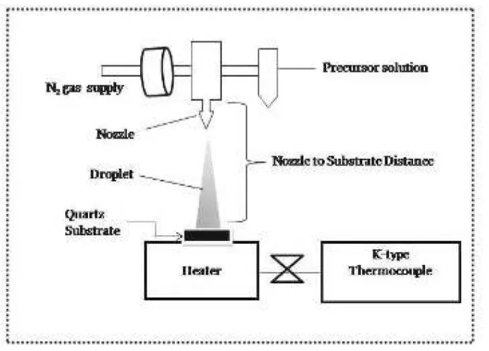
approx. 5 hour, 30 minutes in another sealed glass vial. The two solutions in the sealed gas (fluoride and tin solutions) vial were then added together. A clear solution was obtained after a white precipitate was formed and redissolved in the solution. While other parameters were kept constant, the solution was spray pyrolyzed at NSD of 25-32cm and the substrate temperature was kept at 460oC. The thickness of 100nm was deposited on the quartz substrate at a flow rate of 1.8 ml/min. The schematic diagram of the experimental set up is shown in fig. 1. Before the deposition, substrates were degreased in acetone first, rinsed in absolute ethanol and deionized water several times, and finally dried in Nitrogen gas. In this study, varieties of characterization techniques were used to evaluate the structural, optical and electrical properties of the thin films. The study includes determination of the structural, optical and electrical properties of the films. The morphological features and determination of grain size were investigated by Scanning Electron Microscope (SEM). The band gap of the films was calculated from the absorption edge of the transmittance spectra. The Hall coefficient combined with resistivity measurement set up has been used for studying the electrical properties of the films.
2.1. Characterization of FTO films
An X-ray diffraction (XRD) system in asymmetric out of plane geometry (with 30 kV, 40 mA, Cu Ka radiation at λ = 0.1540598 nm) was used to record the XRD pattern of fabricated films for 2θ values from 20 to 80 degrees [1]. The incidence angle measured with respect to the substrate plane was α = 15 deg. Scanning electron microscopy (SEM) images were obtained using a Zeiss Ultra 55
SEM at 5 kV to characterize the particle morphologies.
Atomic force microscopy (AFM) was performed by model 5000 Digital Instruments system in a contact mode for a 2.5 × 2.5 µ2 array to study surface topology.
A Perkin-Elmer Lambda 900 spectrophotometer collected transmittance spectra T over the wavelength range 200-1000 nm. Absorption coefficient was calculated according to Beer’s law,
3
The optical band gap of the FTO samples was deduced from the absorption coefficient spectrum from equation (1).
The FTO film thickness was determined by cross-sectional scanning electron microscopy (SEM). The film’s resistivity, mobility, and carrier concentration were evaluated by Hall Effect measurements at room temperature with Van der Pauw [5] four-point probe configuration using indium contacts, in a Hall Effect system.
Fig. 1: Schematic diagram of the set up improvised from SPEED and spray pyrolysis set up
3. Results and Discussion
3.1.Structural Properties
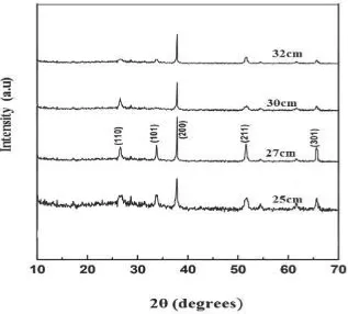
Fig.2 shows the X-ray diffraction (XRD) pattern as a function of SND in FTO thin films. It can be seen that all the films are polycrystalline and contain the SnO2 tetragonal structure. All the films
exhibit the preferred orientation with 110, 101, 200, and 211 planes while all targets are polycrystalline with the highest intensity reflection corresponding to the (211) peak. This finding is in line with [13]. It is seen that crystallinity increases with SND. A similar observation has been observed by [28]. Relatively low-intensity peak from the plane is observed for the film at 25cm SND. The grain size of the deposited films was calculated by the Scherer formula (see equation 1) [29]. XRD peak was found to be between 24-30 nm. For all films, the ‘a’ lattice parameter values are larger than that of the SnO2 powder (a=4.738 Å), and (c=3.187 Å). Although the volume of the unit
cell for all the films grown in this work is observed to be larger than that of the SnO2 powder.
= . (1)
4
Fig. 2: XRD patterns of FTO films deposited at different SNDs
(a) 25cm (b) 27cm (c) 30cm (d) 32cm
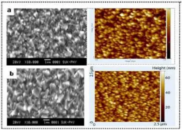
Fig. 3 shows the typical SEM and AFM analysis of FTO films at 27 and 32 cm NSD. Here, the distance between the spray nozzle and the substrate was varied from 25-32 cm, a step of 2. “Although the effect is rather dependent on the other deposition parameters, the surface morphology of the films produced at different distances has shown to be not critical” [10]. However, it is important to identify the distance at which deposition ends up with the formation of a film. “The substrate is completely covered by an almost dense layer of the film when it is close to the spray nozzle. At a further distance, particles are dispersed on the surface while they gradually lose their connectivity and tend to form a powder and moreover, at longer distance, only a small portion of droplets can reach the surface of the substrate and therefore the spray efficiency is considered to be low. When the distance between nozzle and substrate changes, the thermal gradient in the vapor space changes, hence the thermophoretic force acting on the liquid droplet also changed. The expression for thermophoretic force (Fth) is given by (Heavens, 1879), equation (2).
F = πŋρ λ with (r >> 1) (2)
Where rd is radius of the droplet, Td is the temperature of the droplet, ŋ is thermal conductivity of droplet, ρ is the coefficient of viscosity, l is the mean free path of air molecules. Since the radius of the droplet rd is much larger than the mean free path of air molecules, then,
grad T = λλ
&λ , (3)
where Ta is the temperature of an air molecule,λ is the thermal conductivity of droplet. Under a
5
The above phenomenon will give rise to the droplets which are preheated by heat radiation in the air molecules, thus leading to enhancement of the “pyrolytic reaction”.
At SND of 27 and 30 cm, high-quality FTO films were observed; this is attributed to the influence of “heterogeneous reaction” which occurred as a result of proportionate distance from nozzle to the substrate as well as adequate preheating of the droplets in the air. At 32 cm, the water molecules vapourize quickly along the path due to high thermal energy. This situation will give rise to the achievement of pyrolytic decomposition and reaction in a middle way. In another word, “the chemical reaction will be completed in the vapor phase due to inappropriate melting and vaporization of particles; this is the type of reaction is known as a homogeneous reaction because all the reactant molecules and product molecules are in the vapor phase” [10].
Fig. 3: SEM and AFM micrographs of the FTO films as a function of SND
FTO films with poor quality were observed at SND of 25cm or less. The films were characterized by cracked and mud-like morphology. The poor FTO films noticed at these NSD depicts the solvent droplets poor chemical interaction along the path of their journey to the substrate’s surface. The implication of this is that the droplets reaching the substrate would get exploded leaving behind a bunch of damaged film. This circumstance is aggravated by untimely cooling of the aqueous droplets.
Summarily, at the end of the study of structural properties of FTO thin films samples at different NSD, the best samples of FTO thin films were observed at NSD of 27 and 30cm. The findings in this work are relatively similar to those of [12, 10].
3.2.Optical Properties
6
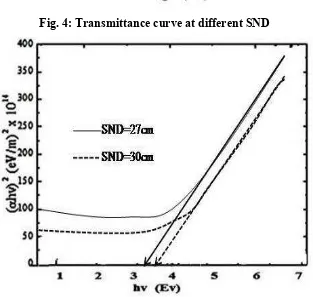
Optical band gap was analyzed from optical data with the expression for optical absorption coefficient ‘a’ and photon energy ‘hυ’ using the relation (3). The optical band gap plot for FTO sample at 25 and 27cm is shown in fig.5. It shows the typical plot of (ahυ)2 vs. ‘hυ’. Extrapolation of the linear portion of the plots to energy axis yielded an average direct band gap value of 3.5eV.
'ℎ) = *+ℎ) − -./ /1 (3)
Fig. 4: Transmittance curve at different SND
7 3.3.Electrical Properties
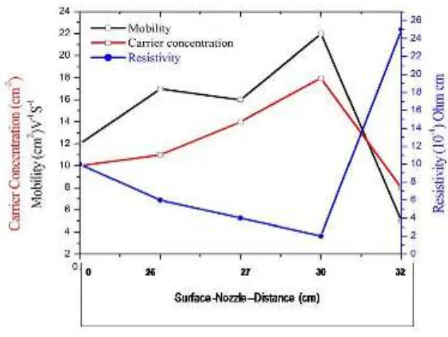
Fig. 6 shows the electrical properties of Nozzle to Surface Distance (NSD) of the FTO films prepared with varying SND. The resistance (ρ), carrier concentration (n), and mobility (µ) are displayed. The SND is an important parameter in controlling the films properties since it is associated with the amount of energy that is given to the droplet to travel towards the substrate. From fig. 6, the resistivity is found to decrease with increasing NSD with the minimum at 30 cm.
Fig. 6: Electrical properties of FTO thin films
8
The Hall mobility and carrier concentration of films follow a similar trend which is opposite to that of resistivity. The value of figure of merit (4.98× 10 ) obtained suggests that the FTO samples fabricated in this work are good candidates for solar cells application [1]. One of the methods of measuring the device performance is through the average figure of merit [1]. Hence, the average figures of merit (2) of the FTO samples was calculated from equation (4).
φ= 645
78 (4)
Where T is the transmittance and9 : is the sheet resistance. The sheet resistance, (9:) is a main
factor for figure of merit, which is calculated by the van der Pauw technique. The average figure of merit of FTO samples at all NSDs was found to be 4.98× 10 . This value depicts high crystallinity and relatively low resistivity which is a requirement for solar cell high performance. This value, when compared with our previous research [1] is a significant improvement 0.023 Ω
.Therfore, the FTO samples grown at 27 and 30 cm NSD are promising candidates for application in dye-sensitized solar cells. Therefore, another research in progress to further improve on the FTO’s figure of merit by employing graphene to enhance its electrical properties.
4. Conclusion
The effect of NSD on the structural, optical, and electrical properties of the FTO films has been grown successfully by homemade spray pyrolysis. As-deposited films were uniform and strongly adherent to the substrate. The properties of the FTO films have been investigated as a function of NSD. The structural, optical and electrical properties of FTO thin films vary with NSD. All films are crystalline with a tetragonal crystal structure. The optical transmittance of the FTO film at SND of 27 and 30 cm have optical transmittance above 80% while the rest have less than 80% transmittance. The optical band gap analysis shows an average of 3.5 eV for NSD of 27 and 30cm. With these properties, the deposited FTO films are very useful in optoelectronic devices. The films electrical properties such as resistivity, electron mobility, electron concentration all vary with NSD. The average figure of merit of FTO samples calculated in this work is 4.98× 10 . It is therefore an improvement when compared with the value of 0.023 Ω obtained in our previous research. The FTO films grown in this study could be a promising ingredient in the fabrication of dyes-sensitized solar cells.
References
[1] Khalilzadeh, F., Oladeji, I., Yusuf, G.T, Nath, J., Nader, N., Vangala, S., Cleary. Shenfield, W., Awodugba, A.O, & Peale, R. Optical and Electrical Properties of Tin Oxide-Based Thin Films Prepared By Streaming Process for Electrodeless Electrochemical (SPEED). MRS Spring Meeting. MRS15-2136423.R1.1-7 (2015).
[2] Endrowednes K., Deok-Woo H., Youl-Moon S., Jae-Eun S., Chi-Hwan H. Structure
and thermal properties of transparent conductive nanoporous F:SnO2 films. Thin Solid Films
517, 4211–4214 (2009).
[3] Martinez, A. Acosta, D.R. FTO Films for Solar Cell Applications. Thin Solid Films, 483 107-111 (2005).
[4] G. J. Exarhos and X. D. Zhou, the Discovery-based design of transparent conducting oxide films Thin Solid Films 515, 7025 (2007).
9
[6] G.T. Yusuf, H.O. Efunwole, M.A. Raimi, O.E. Alaje and A.K. Kazeem. Effect of Al and Mg Doping on Optical Properties of ZnO Thin Films Prepared by Spin Coating DOI: 10.15415/jnp.2014.21005 (2014).
[7] G.T., Yusuf, & Efunwole, H.O. Effects of Dimethylamine (DMA) And Ethylenediaminetetraacetic Acid (EDTA) on Optical, Structural And Morphological Properties of Zinc Oxide Thin Films Prepared By Chemical Bath Deposition Technique Int. Journal of Scientific & Technology Research 1(8), 24- 27(2012).
[8] Masuda, A. Yoshitake, B., Ohji, N., Tatsuki, H., Kato, N., Kazumi, B., Aqueous Phase Deposition of Dense Tin Oxide Films with Nano-Structured Surfaces. Scitech Connect 128-134(2014).
[9] S. Chen, Low emissivity coatings for the improvement of the insulation properties of double-glazing units. Thin Solid Films 77, 127 (1981).
[10] A.R. Babar, S. S. Shinde, A. V. Moholkar, C. H. Bhosale, and K. Y. Rajpure. Structural and optoelectronic properties of sprayed Sb:SnO2 thin films: Effects of substrate temperature and
nozzle-to-substrate distance, Journal of Semiconductors 32 (10) 1-9 (2011).
[11] A. A. Yadav, E. U. Masumdar, A. V. Moholkar, M Neumann-Spallart, K. Y. Rajpure and C. H. Bhosale, ). Effect of Quantity of Spraying Solution on the Properties of Spray Deposited Fluorine Doped Tin Oxide Thin Films. J. Alloys and Compounds 448, 350 (2009).
[12] B. Thangaraju, Fabrication of High-Performance Fluorine Doped–Tin Oxide Film Using Spray Pyrolysis. Thin Solid Films 402, 71 (2002).
[13] A. Goetzberger and C. Hebling, Photovoltaic materials, past, present, future Sol. Energy Mater. Sol. Cells 62, 1 (2000).
[14] G. Frank, E. Kaur, and H. Kostlin, Transparent heat-reflecting coatings for solar applications based on highly doped tin oxide and indium oxide Sol. Energy Mater. 8, 387 (1983)
[15] Chung, Wan-Young, et al. "Tin oxide microsensor for LPG monitoring." Sensors and Actuators B: Chemical 20.2-3 139-143(1994):
[16] Brown, J. R., et al. "Response behavior of tin oxide thin film gas sensors grown by MOCVD." Sensors and Actuators B: Chemical 63.1 109-114 (2000).
[17] P. Nelli, G. Faglia., G. Sberveglieri, E. Cerede, G. Gabetta, A. Dieguez and J. R. Morante, The aging effect on SnO2–Au thin film sensors: electrical and structural characterization.
Thin Solid Films 371, 249 (2000)
[18] Q. Zhao, et al. Tailoring of textured transparent conductive SnO2: F thin films. Journal of
Alloys and Compounds (15) 427–431(2013).
[19] Tatar, D. & Düzgün, B. Pramana The relationship between the doping levels and some physical properties of SnO2: F thin films spray-deposited on optical glass - J Phys 79: 137.
doi:10.1007/s12043-012-0288-3(2012).
[20] A. C. Arias, L. S. Roman, T. Kugler, R. Toniola, M. S. Meruvia and I. A. Hummelgen, The relationship between the doping levels and some physical properties of SnO2: F thin films
spray-deposited on optical glass. Thin Solid Films 371, 201 (2000).
[21] P. S. Shewale, S. I. Patil and M. D. Uplane, Preparation of fluorine-doped tin oxide films at low substrate temperature by an advanced spray pyrolysis technique, and their characterization Semicond. Sci. Technol. 25 (11) (2010)
[22] M. Ruske, G. Brauer and J. Szczrbowski, Thin Solid Films 351, 146 (1999)
[23] Kelly, P.J. R.D Arnell R.D. Magnetron Sputtering: A Review of Recent Developments and Applications. Vacuum Volume) 159–172(2000).
[24] Homma, F., Kentjana, C., & Mooney, M., San Diego. Optics for High-Brightness Synchrotron Radiation Beamlines. California SPIE Vol. 1740, 95-103(1992).
[25] Garcia, M., Maldonado, Castaneda, L., Silva- Gonzalez, R., & Olvera, M.L.SnO2 Thin Film
Gas Sensor Vol. 4, 61-72 (2014).
10
Substrate Deposited By the Spray Pyrolysis Technique Thin Solid Films 515, 8632–8636 (2010).
[27] Perednis, D. & Gauckler, L.J. J Thin Film Deposition Using Spray Pyrolysis Electroceram 14:103. doi:10.1007/s10832-005-0870-x (2005).
[28] Arle, R.N. Khatik. B.L., Effect of Volume Spray Rate on Highly Conducting Spray
Deposited Fluorine Doped SnO2 Thin Films IJCPS Vol. 3 Special Issue – NCETNN 83-88
(2014).
[29] Cullity, B. D., Elements of X-Ray Diffraction, Addison-Wesley Publishing Company Mater. Res. Soc., 32, 242-247 (1978).
[30] Premalal, E.V.A. Dematage, N., Kaneko, S. Konno, A. Preparation of High Quality
Spray-Deposited Fluorine-Doped Tin Oxide Thin Films Using Dilute Di (N-Butyl) Tin (IV) Diacetate Precursor Solutions. Thin Solid Films 520, 6813–6817. (2012).
[31] C-J., Li, C-X, Li, M. Wang. Effect of Spray Parameters on the Electrical Conductivity of Plasma-Sprayed La1-Xsrxmno3 Coating for the Cathode of SOFCS. Surface and Coatings Technology. Surface and Coatings Technology. 198: 278-282(2005).
[32] A. R. Babar, S. S. Shinde, A. V. Moholkar, C. H. Bhosale, and K. Y. Rajpure. Structural and optoelectronic properties of sprayed Sb:SnO2 thin films: Effects of substrate temperature and