Scalable Computing: Practice and Experience
Volume 19, Number 4, pp. 401–422. http://www.scpe.org
ISSN 1895-1767 ©2018 SCPE
MODELLING AND SIMULATION OF GPU PROCESSING IN THE MERPSYS ENVIRONMENT
TOMASZ GAJGER‡ ∗AND PAWEŁ CZARNUL‡ †
Abstract. In this work, we evaluate an analytical GPU performance model based on Little’s law, that expresses the kernel execution time in terms of latency bound, throughput bound, and achieved occupancy. We then combine it with the results of several research papers, introduce equations for data transfer time estimation, and finally incorporate it into the MERPSYS framework, which is a general-purpose simulator for parallel and distributed systems. The resulting solution enables the user to express a CUDA application in a MERPSYS editor using an extended Java language and then conveniently evaluate its performance for various launch configurations using different hardware units. We also provide a systematic methodology for extracting kernel characteristics, that are used as input parameters of the model. The model was evaluated using kernels representing different traits and for a large variety of launch configurations. We found it to be very accurate for computation bound kernels and realistic workloads, whilst for memory throughput bound kernels and uncommon scenarios the results were still within acceptable limits. We have also proven its portability between two devices of the same hardware architecture but different processing power. Consequently, MERPSYS with the theoretical models embedded in it can be used for prediction of application performance on various GPUs.
Key words: Performance simulation, Simulation environment, GPGPU, CUDA
AMS subject classifications. 68M20, 65Y05, 68U20
1. Introduction. Graphics processing units (GPUs) are highly data-parallel devices that are nowadays ubiquitously used for a variety of applications by employing the GPGPU paradigm. GPGPU stands for general-purpose computing on a GPU and refers to the GPU being used to execute tasks, which are not necessarily related to graphics - general purpose tasks, e.g. numerical algorithms, neural networks training, data analysis, and many more. In order to use what the GPU offers effectively, the programmer needs to write a dedicated application. Furthermore, the GPU differs greatly from the CPU both in terms of a hardware design and processing model. It would be of a great help to such a programmer to have a tool that allows creation of a theoretical model of an application and provides means to assess it in terms of computational performance, scalability and behaviour on different hardware units. This becomes even more important when the GPUs are used in highly parallel and distributed environments such as HPC clusters, grids or volunteer computing networks. What is more, according to the recent TOP500 [1] list of the fastest supercomputers, the accelerators (mostly NVIDIA GPUs) are an important component used in 22% of these systems.
Considering NVIDIA’s dominance in this field, the size of the CUDA community and maturity of available software tools, we have decided to focus our efforts on the NVIDIA GPUs. Nevertheless, we have developed a generic solution for simulation of running applications on GPUs. Use of a simulator equipped with a proper theoretical model, such as MERPSYS described later, may be beneficial in many ways, one can use it to analyse the behaviour of an application in hardware setups which may be unavailable for testing purposes, such as before purchasing. It also allows to exceed limits imposed by the hardware, e.g. assess the relation between execution time and data size for very large data sets. Despite providing estimations for application execution time, a simulator may also compute the predicted energy consumption or failure chance. These values may be then used for multi-criteria optimisation [44], including energy efficiency and reliability. For a GPU, a simulator can allow easy assessment of application execution using various configurations such as grid configuration or application parameters. When searching for an appropriate theoretical model one should consider only these of acceptable (preferably as high as possible) accuracy, but this is not the only expected trait. Ease of use, the possibility to extend and customise the model are important as well and lastly, the closer the model resembles the actual processing that happens on the GPU, the better. The complexity of the GPU hardware and abundance of internal parallelism makes such a theoretical model harder to develop, but as we will further show in Section 4.1,
‡Department of Computer Architecture, Faculty of Electronics, Telecommunications and Informatics, Gdansk University of
Technology, Narutowicza 11/12, 80-233 Gdańsk, Poland
this is still a manageable task. We have analysed existing solutions, based on which we propose a performance model for a GPU.
In this paper we contribute by incorporation of modelling parallel processing on a GPU into an existing simulator – MERPSYS [15], validate the model against real results for a parallel GPU-enabled application with various launch configurations on three different GPUs and emphasise benefits from using MERPSYS for simulation using various GPUs from its database. Details of our contribution are described in the context of introduced models in Section 3.3. The paper is organised as follows: Section 2 explains important aspects related to the GPU processing and briefly describes the MERPSYS framework, Section 3 lists related work and motivations for developing the modelling solution. In Section 4, we propose our own solution, explain it in detail, and show its implementation in Section 5. Section 6 describes our testbed, testing methodology, validation of the model, and presents the results. Finally, Section 7 summarises results and outlines the proposed direction of future research.
2. Background.
2.1. GPU architecture and programming model. GPU is a many-core device that exemplifies a SIMD (Single Instruction Multiple Data) architecture type per Flynn’s taxonomy [32]. Although the GPU itself does not contain vector units but rather simple cores capable of executing one instruction on a single operand at a time (or two instructions if we consider FMAC operations), it acts in a very similar manner. All the threads comprising a single work group (called warp) in a single clock cycle execute the same instruction on different operands, that is why NVIDIA describes this architecture as SIMT [39] (Single Instruction Multiple Threads). This term is obviously a direct derivative of SIMD but expresses the internal architecture of the device more clearly - multiple threads executing an instruction instead of a single thread executing it on a wide register containing multiple operands. GPU is perfectly suited for handling tasks that are highly data parallel and compute intensive, yet simple in terms of the control logic.
A CUDA program is heterogeneous in its nature and consists of two parts: one that executes on the CPU and one that is offloaded to the GPU. Upon program launch the code is executed by the CPU until a kernel invocation is encountered. When it happens, two important parameters are specified: grid size and block size [37]. As the grid may be comprised of many threads, it is logical that only a limited number will be loaded to the Streaming Multiprocessors (SMs) at a given time, allocation is done at the block level and once a block finishes its execution a new one will be scheduled. This process continues until all of the blocks are processed [19].
Without going into deeper details, from our perspective the following facts are important: 1. SM may hold a limited number of blocks at a time;
2. blocks have their requirements for shared memory and registers which need to be allocated from the pool available on the SM;
3. threads are executed in groups of 32, called warps;
4. there are constraints regarding maximum number of active warps as well as rules affecting warps execution;
5. SM can perform zero-overhead context switches between warps.
The above directly affect the capability of the SM to execute the instructions effectively. If the number of active warps is not large enough to cover the stalls (caused by memory accesses, conditional branches resulting in warp divergence, etc.) then performance will be suboptimal [45]. The process of calculating the number of threads that may be loaded to a single SM considering shared memory and register constraints is called occupancy calculation. Shortly speaking, if the occupancy is poor then likely the performance of the application will decrease. It should be noted, however, that increasing occupancy may not lead to any performance gains or may even result in a performance degradation [46] because of an increased contention for shared resources as was experimentally proven in [6]. It is also possible to achieve optimal performance with a very low occupancy if thread granularity (number of instructions executed per thread) is sufficient [50]. Given all these, it is clear that the effectiveness of warps execution depends on the characteristics of the specific kernel.
code is an intermediate representation of a program and an abstraction over GPU architecture that is not tied to any hardware type, thus it does not directly resemble the instructions that are executed by the GPU. It is ultimately translated into a machine code (cubin object) either by nvcc in a separate compilation step or by leveraging just-in-time compilation by the CUDA runtime driver upon being scheduled for launch on a specific device [38]. This allows a high level of interoperability between varying GPU architectures. SASS is the machine code for GPU, generated for a specific architecture and maps directly to instructions being processed by the functional units. It can be either generated directly bynvccduring the compilation process or, as it was already mentioned, generated on-the-fly from PTX source code.
2.2. MERPSYS. Developed at the ETI faculty of Gdansk University of Technology, MERPSYS1 [13, 15]
is a simulation environment for distributed systems that allows its users to predict execution time, power usage and failure probability of their applications. The application is described in a form of Java code imbued with special functions implementing communication (MPI-like) and computation primitives. The system is modelled as a hierarchical structure of components representing computational devices and interconnects, each of them having its own characteristics defined. It consists of four software components: GUI, server, database and simulator. Block based representation [12] is employed as a theoretical concept behind the application model, the environment provides a set of extensions to the Java language that allow to define computation and communication blocks while preserving the original structure of the code. An application model can be expressed in Java with additional message passing communication primitives using properly parametrized (input data size, operation type, etc.) MERPSYS-specific constructs in place of actual computation or communication code.
A system model is created by selecting hardware components and placing them in the editor’s workspace. It may consist of several nested levels, e.g., two machines connected using an InfiniBand network and inside each of them a GPU and a processor connected via a PCIe bus. The hardware model is a term used to describe the characteristics of a given hardware setup. A model has special functions associated with it that reflect, e.g.: power usage equation for an active or idle component, communication time for point-to-point, scatter or gather operations, etc. These functions are then used by the simulator to calculate the effective time taken by various operations. Hardware components have attributes that describe their characteristics. A database of hardware components is provided, that can be extended with new records. It should be further noted that the hardware model is sometimes referred to as a computational model. For each computational component a user defines an arbitrary number of labels that are used to tie application and hardware models together. They are used in the application model to mark parts of the code representing distinct processes or threads and allow the scheduler to map them to the hardware components. A simulation configuration screen also allows to define attributes that are passed to the application model, an example of such may be data size, block configuration of a GPU, etc. A request to launch a simulation is passed from GUI to the server which in turn directs it to one of the simulators connected to one of its simulation queues [13]. The simulation queue to be used may be specified as well.
MERPSYS was successfully used by its authors to model execution time, energy consumption and reliability of divide-and-conquer (DAC [18, 13]) and geometric single program multiple data (SPMD [13]) applications [16], K-means algorithm [17] and volunteer computing systems [14]. For a more detailed description providing better insight into the whole MERPSYS environment see [15].
3. Related Work.
3.1. GPU performance models. When considering performance models targeted specifically at GPUs, several approaches are to be distinguished, three of the most common are [30]: analytical methods, quantitative and compiler-based methods, statistical and machine learning methods. The first kind focuses on creation of a theoretical model for a kernel execution expressed as set of equations and feeding it with parameters obtained by direct analysis of the kernel’s code and the underlying hardware. Amaris et al. have proposed an analytical model [2] based on BSP [49], that estimates kernel execution time using an equation combining global and shared memory access times, with computation time and available GPU hardware resources. Another model [23] focuses on highly parallel aspects of GPU processing, discerning ones originating from parallel execution of
1
warps and memory accesses. It enumerates as many as 21 distinct parameters obtained via source code analysis, microbenchmarking, or defined by user. These are then used to estimate kernel’s execution time.
The model proposed by Volkov [51] leverages Little’s Law by defining the parallel process using three metrics: warp latency bound, warp throughput bound and occupancy. Execution of a kernel is modelled at a warp level in the scope of a single SM with the findings extrapolated to reflect the overall kernel execution time. The model focuses on obtaining a key metric describing the parallel process - a warp throughput, from which the total kernel execution time can be derived. Concurrency in this case is synonymous to occupancy through the number of active warps residing at an SM at a given time. Furthermore, an assumption is made that both the occupancy and the throughput are sustained for the entire time of the kernel’s execution. An important part of the model are the bounds for warp throughput and latency, warp throughput is limited by throughput bound imposed by the hardware and its latency may not be lower than the one resulting from the instruction sequence comprising the kernel. Warp latency bound is obtained by direct inspection of the compiled kernel assembly code. Warp throughput bound is calculated based on requirements for resources available on the SM. Quantitative methods, on the other hand, evaluate the characteristics and behaviour of a given kernel either by measuring or microbenchmarking kernel execution on actual hardware or by executing it, or parts of it, in a GPU simulator. These are often integrated into a compilation process of a kernel and are more automated than analytical ones. Examples include the following: an automated approach where the kernel is analysed to create a work flow graph [5] that focuses on measuring warp and instruction level parallelism, that is later parametrized to reflect execution process on a specific GPU unit; a microbenchmark based [53] method where instructions are extracted directly from the compiled source code of a kernel, backed by a functional simulator for memory accesses; Ocelot dynamic compilation framework [27, 28] leveraging PTX representation of a kernel, that is transformed into a form feasible to be modelled on a single CPU thread. Lastly, an interval analysis [24] technique, which is based on an assumption that by locating events causing performance degradation (memory stalls, cache misses, etc.), one can reason about the overall execution time of a kernel.
Statistical and machine learning methods [25, 52, 31] are often implemented as separate frameworks that are highly automated and require additional training so that the neural network correctly recognises patterns and behaviour of the kernel code. The network learns the kernel’s instructions composition given a set of input data and is then able to reason about the performance of subsequent kernel executions for different launch configurations. Consequently, they provide a complete simulation environment on their own and are not suitable for developing a new model that could be used within MERPSYS. Given the aim of this work is extending MERPSYS with a performance model for a GPU, we find them not relevant in our analysis.
3.2. GPU modelling in general-purpose simulators. General-purposesimulators are not tied to any specific device type or programming language and provide means to perform various kinds of simulation for many processing paradigms on parallel and distributed systems. Designing an application for such environments is not a trivial task as one needs to consider execution time, energy efficiency, reliability, maintainability and many other factors [48]. This is why most of the simulators a layer of abstraction over the actual hardware, what is a good thing when we consider a use case like modelling a complex grid system, but it may also be a significant drawback if one needs to model the parallel process on a specific hardware unit with a greater detail. All of further mentioned simulators implement the discrete-event simulation model [43], which means that the entire process of simulation is governed by events being processed and passed between entities. Such an event may represent a computation, communication, synchronisation or a resource access, with the details specified by the simulation environment itself. We have looked at the following tools with the focus on GPU simulation: GridSim [8], SimGrid [42, 21], CloudSim [9, 41, 47], GSSIM [29, 7], and MARS [20]. Table 3.1 summarises their suitability for this purpose, a general overview of their functionality was given in [15].
Table 3.1
General-purpose simulators comparison
Simulator Level of detail available for modelling a
hardware component Suitability for GPU modelling
GridSim Poor - computational power defined in terms
of MIPS or SPEC rating. Not with the required level of detail.
SimGrid High - complex analytical models may be used.
Theoretically yes, would require more in-depth investigation of the possibility to extend the existing framework with a custom computational resource.
CloudSim High if extensions to the framework are used. Yes, but not with the required level of detail. GSSIM Plugins that take many factors into account
may be written to describe the performance.
Possibly, by writing plugins to define complex application performance models.
MARS
Task modules execute logs containing MPI call traces. There’s no room for
customisation.
Not at all.
of the model by substitution of other hardware such as GPUs and repeating simulations, easy modification of formulas modelling execution and communication times, as well as relevant constants and coefficients.
3.3. Contributions of this work. Contributions of this work are as follows:
• We have incorporated the model proposed by Volkov [51] within the MERPSYS simulator [15], showing that it is well suited for practical implementations. We have used a simplified version of this model by reducing the scope of hardware units considered to CUDA cores, schedulers, and global memory system, for which we decided to use a trivial non-parametrized access model. For this version, we provide a complete set of equations (Eqs. 4.1 - 4.6) together with a detailed description of input parameters, creating an easy to grasp explanation of all the building blocks of the model.
• We have also extended the model with a scaling parameter, allowing to fine-tune it to better fit hardware and kernel characteristics. We propose Eq. 4.5 for calculating global memory bandwidth and introduce data transfer time calculation, whilst the original model considered only kernel execution time.
• We show that for the considered model configuration derived from results on one GPU of a given architecture can be directly applied to another GPU of the same architecture, introducing only the second GPU’s specifications into the model. This makes the MERPSYS environment with the model deployed in it a suitable tool that is able to verify performance of a given application on potentially several cards without even having physical access to them.
4. Proposed Approach. Compared to other general-purpose simulators, MERPSYS is a much better fit for GPU modelling. It is mainly because of the very high level of detail available when modelling a hardware piece combined with a possibility to add custom functions describing device’s behaviour. Hence, the computational devices are highly customizable which allows implementation of complex analytical models like the one being described in this section. Additionally, the hardware (computational) model may be customised to use additional data needed for GPU modelling. This data may be specified in the application model, which allows for easy parametrization of simulation runs. Another advantage is an extensible database of hardware components and ease of hardware model customisation, which allows for convenient evaluation of various setups. These can be activated just by selecting other GPUs, that have all the parameters in the database, through a graphical interface.
we explain the meaning of each of these elements and the approach used to determine their values. Since the entire model is based on a concept of modelling a concurrent process in terms of a warp being executed on a Streaming Multiprocessor (SM) and the metrics are calculated for that single warp, it is required to extrapolate the findings to reflect the actual number of warps that were executed on the GPU and thus compute the result. For this purpose, Eq. 4.2 is used that takes as an input the launch configuration of a kernel i.e. the sizes of grid and block, and the result is the total number of warps that were launched to process the kernel.
Tk =
WL
WT h×SM s×SMclock×λk
(4.1)
WL=grid size× ⌈
block size warp size ⌉
(4.2)
WT h≈min (
occupancy
Latbound , T hbound )
(4.3)
where: Tk – estimated kernel execution time [s]; WL – number of warps launched; WT h – processing rate of warps [1 / cycle];SM s– number of streaming multiprocessors;SMclock– SM core clock [cycles / s];λk – scaling parameter; grid size– number of blocks in a grid;block size – number of threads in a block; warp size– 32 for all GPU architectures;T hbound – throughput bound [1 / cycles];Latbound– latency bound [cycles].
SM s andSMclock parameters are needed to extrapolate the model from a single warp in scope of a single multiprocessor to one that fits the processing model of the GPU. These two parameters, when multiplied, yield the processing power of the entire device in cycles per second. The λk value is a ratio between estimated and measured execution times that adjusts the model to fit the characteristics of a given kernel launched on a specific device architecture. It shall be obtained experimentally by measuring the execution time of a real application combined with running a simulation with an initial model. Once calculated the newλk can be used to perform simulation across varying data sizes and different GPUs. It was experimentally proven by the authors of another model [2, 3] that a single λk value is sufficient for accurate simulations in scope of a single device architecture. When used for a different architecture the accuracy of the model drops and it is advised thatλk is recalculated. To calculate theλk we divide the estimated execution time, by the measured one: λk= Testimated
Tmeasured.
Calculation of warp throughput, the most essential part of the model, as given by Eq. 4.3, is the most challenging task. Three parameters need to be extracted from the kernel code in close consideration of a specific GPU architecture that one intends to model. These parameters are warp latency and throughput bounds, and the achieved occupancy, we will describe them in detail in subsequent sections.
4.1.1. Occupancy. The first method of retrieving the parameters needed for occupancy calculation is to compile the code with verbose ptxas output, this is done by passing ’-Xptxas -v’ command line option tonvcc [38]. A sample result is shown in Listing 1. It tells us that the kernel uses 8 registers per thread and does not use any shared memory, otherwise information about the amount of shared memory used would be included in the output. cmem stands for constant memory and does not concern our analysis. Having determined the number of registers and amount of shared memory required, we enter these together with threads per block count (block size) into the NVIDIA occupancy calculator [34] to get the theoretical occupancy. Another way is to profile the application, NVIDIA Visual Profiler not only displays the values of shared memory and registers used but it is even capable of calculating both the theoretical and achieved occupancies.
Listing 1
Verbose ptxas output for saxpy2 kernel p t x a s i n f o : Function p r o p e r t i e s f o r saxpy2
4.1.2. Latency bound. We construct an execution graph of the kernel with nodes representing instruc-tions and edges representing latencies as shown in Volkov’s work [51] and then apply a critical path method to it to find the latency. Critical path is the latency bound only if we assume that all of the warps are the same - they execute the very same instructions, so this approach will not work if there is a substantial control flow divergence in a kernel. In such a case, a different set of instructions resulting from different branches being executed should be considered.
The graph considers latencies of the following kind: register dependencies and thus instruction execution latency, instruction issue latency, and memory stalls to describe how the instructions comprising the kernel are depend between themselves. This approach is valid because there is no out-of-order execution present in the GPUs, meaning that the sequencing of the instructions is maintained in a strict order. It is also more precise than when making an assumption that a kernel is a simple sequence of dependent instructions as in [2, 11, 40] and simply summing the latencies of all instructions comprising the sequence, treating the result as a total cost in clock cycles of executing this kernel by a single warp. The latter approaches fall short because there are independent functional units within the SM, which results in latency hiding, e.g. in case of waiting for memory accesses. Furthermore, even in the case of a single functional unit type the instructions are processed in a pipelined-based manner and thus ILP (Instruction Level Parallelism) exists.
Volkov reports [51] that there are two other types of latency, the latency between two independent in-structions from a single warp, called ILP latency and latency resulting from a replacement of a terminated thread block, we address both of these. What is more, depending on the architecture, multiple warp schedulers per SM may be present and two instructions per warp may be issued every instruction issue time if mutually independent instructions are available for execution. The effect of dual issue is considered as well, in which case the ILP latency is expressed as 0 cycles. We omit double precision and special function units, both of which have their own pipelines with different latencies for various instructions. Moreover, our approach to modelling global memory accesses is simplified as we do not consider gradual saturation effect [51], which manifests itself in a form of increasing memory access latency as the number of memory transaction increases and memory bus gets saturated. It should also be noted that the modelling of shared memory accesses was omitted. These omissions do not affect results of our work as we have deliberately chosen a simple kernel, which does not make use of aforementioned functional units. Furthermore, the model is designed in such a way that it may easily be extended with these elements in the future.
4.1.3. Throughput bound. To obtain the throughput bound, each of the hardware resources available on the SM must be considered separately, including: CUDA cores, Special Function Units (SFUs), double precision units, schedulers, and global and shared memories. We will narrow our analysis to three of them as denoted by Eq. 4.4. The tightest bound, that is the highest number of cycles required to execute the warp’s instructions due to a limited processing power of the functional units, is selected as the limiter of the performance and then a reciprocal is calculated to obtain the bound represented in warps per cycle.
T hbound≈ 1
max(Wsz×IN SCU DA
CU DA cores ,
IN Sissued
schedulers,
GM embytes
GM embw
) (4.4)
GM embw≈
GM emclock×bus width8 ×data rate
SM s×SMclock (4.5)
where: Wsz – warp size;IN Scuda – number of instructions to be executed by CUDA cores; IN Sissued – total number of instructions issued (including dual-issues and re-issues); CU DA cores – number of CUDA cores available on the SM; schedulers – number of schedulers available on the SM; GM embytes – number of bytes transferred with global memory for each warp [bytes]; GM embw – peak throughput of the memory system per SM [bytes / cycle]; GM emclock – global memory clock [Hz]; bus width – global memory bus width [bits]; data rate – data rate multiplier depending on the kind of memory used.
Table 4.1
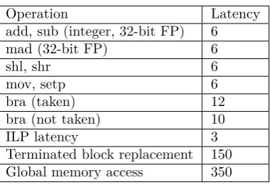
Instructions latencies for Maxwell architecture
Operation Latency
add, sub (integer, 32-bit FP) 6
mad (32-bit FP) 6
shl, shr 6
mov, setp 6
bra (taken) 12
bra (not taken) 10
ILP latency 3
Terminated block replacement 150
Global memory access 350
access times, varying instruction latency depending on the instruction sequence and other effects. Based on papers [4, 51] and additional reasoning, Table 4.1 presents latencies we assumed in this work. For latencies of Tesla, Fermi and Kepler architectures see [4], for Pascal and Volta see [26]. For a detailed information regarding meaning of the mnemonics refer to [36].
There are two sets of parameters in Eq. 4.4. The first one is related directly to the hardware characteristics of a given device, it includes: warp size, number of CUDA cores and warp schedulers, and the throughput of the global memory. At the time of writing the warp size is a constant value of 32 for all GPU architectures. The number of CUDA cores and warp schedulers may be obtained from GPU hardware specification. Theoretical bandwidth of the GPU’s global memory available per single SM every cycle is given by Eq. 4.5, for which all the parameters are available in hardware specification except the data rate that is derived from memory type and equals 2 or 4 respectively for GDDR3 and GDDR5 [33]. Although the peak bandwidth is not sustainable in practice for the entire execution of a kernel because the memory clock may drop due to dynamic frequency scaling and furthermore would require an ideal access pattern and sufficient occupancy, a value close to this theoretical limit is attainable [51]. Considering this fact, we use this bandwidth in the proposed model. What is more, we do not differentiate between loads and stores and assume them to behave in the same way. Additionally, we limit the model to a scenario where there are no cache hits and the accesses are fully coalesced. If we were to include the possibility of cached accesses in the model then we would need to consider the fact that depending on the device architecture accesses to global memory are cached in L1 and L2 caches, hence the number of cache hits should be subtracted from the actual number of DRAM accesses. The ratio of cache hits could be obtained by launching the application in a profiler [11].
The second set of parameters: IN SCU DA,IN SissuedandGM embytesdescribes application execution char-acteristics, all three are extracted directly from compiled SASS code of the kernel, description of these follows. To calculate the number of CUDA core instructions we count all occurrences of operations that are executed using these cores: FP32, INT32, logical, etc. Getting a sum of all instructions that were issued is a little more demanding because dual-issues and re-issues of instructions need to be accounted for. In the former case, two instructions are issued in a single issue cycle and hence are counted as one. In the latter, a single instruction must be counted multiple times depending on the number of re-issues. A re-issue typically occurs when there are bank conflicts when accessing shared memory or when an access to global memory is uncoalesced and must be split into several separate transactions. This also affects number of bytes transferred per warp, for example when fetching a single 32-bit value per thread, a stride of two would result in 256 bytes transferred instead of 128 and a single additional re-issue of memory transaction instruction, stride of 4 would cause 3 additional re-issues and increase the number of bytes to be transferred to 512. Numbers of functional units and clock values for the devices as listed in Section 6.1 were obtained from vendor’s documentation and usingndivia-smi [35].
[12]:
Tc=ts+ n
bw×λc
(4.6)
where: Tc – data transfer time;ts– startup time;n– data size;bw – bandwidth;λc – scaling parameter. Startup time is the time needed to initiate data transfer that depends on latency and runtime overhead, it can be measured by sending a very small data packet. Bandwidth is dependent on the configuration of the PCIe bus that connects the devices, for example a theoretical bandwidth of PCIe v3.1 16x bus in single direction is 16GB/s or 15.8 GB/s if we consider 128b/130b encoding. Furthermore, we have noticed that the bus is better utilised for larger data sizes but even for the largest transfer of 2GB the throughput was noticeably lower than the theoretically achievable one. Due to this fact, in our implementation we introduce an additional scaling parameterλcto Eq. 4.6 that allows us to fine-tune the link bandwidth so that it reflects the actual characteristic of a given hardware setup.
Note that both the λc andts will have different values for each transfer direction. The scaling parameter can be obtained similarly to the one for the kernel execution time (λk), i.e. by dividing the estimated transfer time by the measured one. To get the value of the bandwidth parameter we first need to determine the PCIe configuration, for this purpose we have used nvidia-smi. Having obtained these two values, we can refer to hardware documentation to get the bandwidth parameter.
5. Implementation. It is easiest to present how the performance model is constructed by example. For this purpose we usesaxpy2 kernel (Listing 2) that is a slightly modified version of a kernel from the blog post [22]. The main difference when compared to a regularsaxpy is that instead of a single multiplication an equivalent number of additions is performed, this allows us to benchmark kernels of various compute intensities. The highlighted part of the code is responsible for a compute intensity of the kernel, i.e. the number of arithmetic instructions executed by each warp. Input data size is determined by the number of elements in the vectors as: number_of_elements_per_vector×2×4 Bytes.
Listing 2
Testbed CUDA kernel
__global__ v o i d saxpy2 ( i n t n , i n t a , f l o a t ∗x , f l o a t ∗y ) { i n t i = b l o c k I d x . x ∗ blockDim . x + t h r e a d I d x . x ;
i f ( i < n ) {
f l o a t v a l = x [ i ] , tmp = 0 ;
#pragma unroll 1
for ( int cnt = 0 ; cnt < a ; ++cnt ) tmp += val ;
y [ i ] += tmp ; }
}
To accurately determine the kernel’s instruction composition, we cannot simply analyse the C or C++ source code since we do not know the optimisations that took place and thus the actual instructions that were generated by the compiler. For this purpose we need to analyse SASS code (see Section 2.1.1), to extract it from a compiled binary file we usecuobjdump[36]. Listing 3 is a SASS representation of thesaxpy2 kernel that was compiled forsm_52, for the sake of brevity we skip the irrelevantNOPinstructions from the very end. The highlighted part represents the loop governing the kernel’s arithmetic intensity.
Listing 3
SASS representation of the saxpy2 kernel MOV R1 , c [ 0 x0 ] [ 0 x20 ] ;
S2R R0 , SR_CTAID.X; S2R R2 , SR_TID .X;
ISETP .GE.AND P0 , PT, R0 , c [ 0 x0 ] [ 0 x140 ] ,PT; @P0 EXIT ;
MOV R3 , c [ 0 x0 ] [ 0 x144 ] ; SHL R6 , R0 . r e u s e , 0 x2
ISETP . LT .AND P0 , PT, R3 , 0x1 , PT; SHR R7 , R0 , 0 x1e ;
IADD R2 . CC, R6 , c [ 0 x0 ] [ 0 x148 ] ; MOV R0 , RZ ;
{ IADD .X R3 , R7 , c [ 0 x0 ] [ 0 x14c ] ;
@P0 BRA 0 x100 ; }
{ MOV R5 , RZ ; LDG. E R0 , [ R2 ] ; } MOV R4 , RZ ;
IADD32I R4, R4, 0x1 ;
ISETP.LT.AND P0, PT, R4, c [ 0 x0 ] [ 0 x144 ] ,PT; { FADD R5, R0, R5;
@P0 BRA 0xd0 ; }
MOV R0 , R5 ;
IADD R2 . CC, R6 , c [ 0 x0 ] [ 0 x150 ] ; IADD .X R3 , R7 , c [ 0 x0 ] [ 0 x154 ] ; LDG. E R5 , [ R2 ] ;
FADD R0 , R0 , R5 ; STG. E [ R2 ] , R0 ; EXIT ;
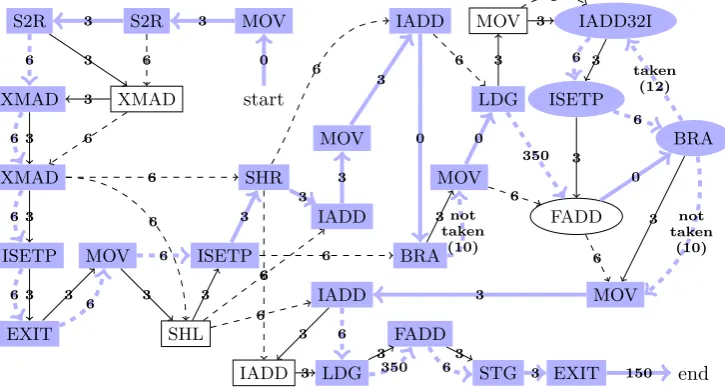
5.1. Creating kernel execution graph. To construct an execution graph ofsaxpy2 kernel we start off by creating a directed graph representing the sequence of instructions comprising the kernel based on Listing 3. Each instruction is a single node, additionalstart andend nodes mark respectively the entry and exit point of the kernel. Edges represent the dependencies between the instructions and are labelled with latency values from Table 4.1. Straight, solid arrows are used for the ILP latency, which equals 3 cycles for Maxwell architecture. There are total of 3 dual-issues, these edges are labelled with 0. The next step is to include latencies from register dependency, these are shown as dotted arrows. We do this by reading the SASS line by line and verifying whether any of the input registers of the current instruction has its value written to by one of the preceding instructions, if so then a register dependency exists and we add a new edge connecting the predecessor with successor labelled with latency value of the preceding instruction. If this instruction is a memory access, then we use the latency of the storage area being referenced, which in case of this kernel is always the global memory as cache hit ratio equals 0%. This is true because there is no re-use of data - each element is accessed by a single thread and exactly once. We verified correctness of this assumption by inspecting the profiler output for this kernel regarding the memory throughputs. Lastly, we label the inbound edge of the virtual end node with a terminated thread block replacement latency.
Once the graph is complete and labelled we use the critical path method to find the latency bound of the kernel. Figure 5.1 shows the resulting graph with critical path highlighted in blue. The part of the graph where nodes are ellipses is the computational loop, which may execute multiple times depending on the compute intensity parameter passed to the kernel. When calculating the latency bound, the critical path of the loop needs to be multiplied by the number of loop iterations. The final equation for latency bound is as follows: latency bound= 92 + 700 + 150 + 24a= 942 + 24awhere the first term is sum of instructions’ latencies, the second one is latency of memory accesses, the third is thread block replacement latency, and the fourth one is latency of the loop multiplied by the compute intensity parameter ’a’. We have created and analysed the graph manually, but creation of an automated tool is entirely possible.
5.2. Obtaining throughput limits. As the first step in throughput limit calculation for the saxpy2
start MOV S2R S2R XMAD XMAD XMAD ISETP EXIT MOV SHL ISETP SHR IADD MOV IADD BRA MOV LDG MOV IADD32I ISETP FADD BRA MOV IADD IADD LDG FADD
STG EXIT end
0 3 3 3 3 3 3
3 3 3 3
3 3 3 3 0 3 0 3 3 3 3 0 3 3 3 3 3 3 3 150 6 6 6 6 6 6 6 6 6 6 6 350 6 6 taken (12) 6 6 6 6 6 6 6 not taken (10) 6 6 not taken (10) 350 6
Fig. 5.1.Execution graph for saxpy2 kernel
the assembly listing (Listing 3) or based on the kernel execution graph (Fig. 5.1). In our example, we have 23 CUDA core instructions that are executed once and 4 instructions in a loop, so the resulting equation is: IN SCU DA = 23 + 4a. It should be noted that in this kernel everything except memory accesses is processed by CUDA cores, this would not be the case if there were any instructions designated for a double precision or SFU units. When getting the number of instructions issued we must remember to address the dual-issues and re-issues. In our kernel, we have 3 accesses to global memory, all three are fully coalesced so there are no re-issues taking place. There are 3 dual-issues, each resulting in a pair of instructions being issued together during a single cycle.
Summing up, we have 23 CUDA core instructions issued once and four of these in a loop, three memory instructions, and three dual-issues which we subtract from the total number, so we get: IN Sissued = 23 + 3−3 + 4a= 23+4a. The number of bytes transferred to and from a global memory depends on four factors: the number
of the memory access instructions, cache hit rate, operand size, and access pattern. Thesaxpy2 kernel contains 3 memory access instructions: two loads and a single store, but for the sake of brevity we do not differentiate between these two as the difference is marginal. In all three cases, a single 4-byte value is accessed per thread and as was mentioned in preceding paragraph, the accesses are fully coalesced so there are no redundant memory transactions when accessing the data, this gives us: GM embytes = 3×4 bytes×32 = 384bytes. Furthermore, there are no cache hits hence all these bytes are accessed directly in the global memory and we can entirely omit both the L2 and L1 caches. If this was not the case then we would separately consider a fraction ofGM embytes equal to cache hit ratio as being accessed from cache, which has a higher throughput than the global memory. Now that we have all the throughput related parameters extracted from the kernel we need to list those specific to the device the application will run on, which is NVIDIA GeForce GTX 970 in our case. The first two parameters can be obtained directly from card specifications shown in Section 6.1, compute capability of our card is 5.2, hence we have: CU DA cores= 128,schedulers= 4. The third parameter - bandwidth of the
global memory can be calculated using Eq. 4.5 substituting the required values as: GM emclock = 1753M Hz, bus width= 256 bits, data rate= 4,SM s= 13,SMclock= 1253M Hz. This gives us: GM embw= 13.78Bytes
cycle The final step is to gather up all these parameters and substitute them to Eq. 4.4:
T hbound≈
1
max(32×(23+4a) 128 ,
23+4a 4 ,
384 13.78
)
Fig. 5.2.Hardware units with customised attributes: GPU (left), interconnect (right)
transfer time in function of its size for both directions as shown below.
THost to Device= 3.9687×10
−6+ n
15.8×109×0.689 andTDevice to Host = 5.1569×10
−6+ n
15.8×109×0.653.
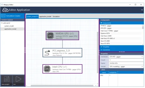
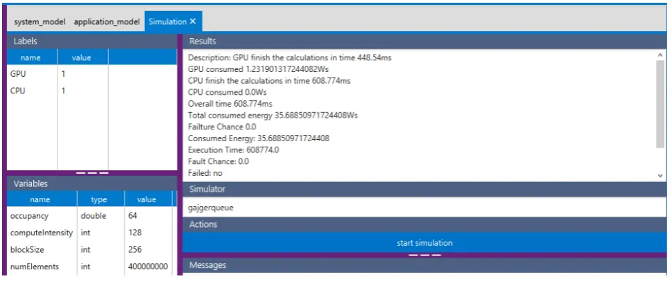
5.4. Incorporating the model within MERPSYS. In this section, we show how the theoretical model was implemented in MERPSYS. At first, we demonstrate how to create a system model representing our testbed, including the creation of new hardware units. Then we proceed to computational model definition, i.e. the programmatic representation of what was shown in previous sections. Next, we move to the application model definition, which will represent the CUDA application being modelled, explaining how all these pieces are tied together and finally elaborate on how to customise the application launch parameters and execute the simulation. Creation of hardware units that are customised with parameters required by our theoretical model was the first implementation step. All previous measurements were performed usingGTX 970 andPCIe v3.1 16x. For these two devices we have created a representation in MERPSYS’ database as shown in Fig. 5.2. It should be further noted that theλc parameter from Eq. 4.6 was included as an attribute of the PCIe hardware unit. We assumed that the effective bus utilisation is a parameter of the hardware itself and its value does not change for different application types if the memory transfers are performed using the same functions. Shall a requirement for this parameter be customizable via application model arise, it can be moved there and passed in the function calls the same way it was done for kernel parameters, as shown in Section 5.4.2.
Fig. 5.3.Testbed configuration in MERPSYS system model editor
Figure 5.3 is a screenshot from the editor application showing the created model, GPU unit is selected with its properties visible on the right side, moving from the top to the bottom:
1. Hardware - hardware unit represented by this element, in our case the GTX 970 GPU visible on the left of Fig. 5.2;
2. Count - the number of hardware units of a given type, for example in a multi-GPU setup we could set the count to 2, 3, 4, etc.;
3. Name - displayed name of the element;
4. Model - computational model connected to the element, in our case the one from Listing 4, description of which will follow;
5. Labels - labels assigned to the element, these form the connection between hardware and application models. Name is the identifier of the label and multiplicity denotes the number of processes with this label that may be executed on a single unit of this type.
Listing 4
Part of the computational model f u n c t i o n getTimeGPUModel ( params ) {
var warpsLaunched = getWarpsLaunched ( params . g e t ( ’ g r i d S i z e ’ ) , params . g e t ( ’ b l o c k S i z e ’ ) ) ;
var throughputBound = getThroughputBound ( params . g e t ( ’ CUDACoreInstructions ’ ) , params . g e t ( ’ i s s u e d I n s t r u c t i o n s ’ ) , params . g e t ( ’ GMEMBytesTransferred ’ ) ) ; var latencyBound_WPC = params . g e t ( ’ occupancy ’ ) / params . g e t ( ’ latencyBound ’ ) ; var warpThroughput = Math . min ( latencyBound_WPC , throughputBound ) ;
var execTime_cycles = warpsLaunched / ( warpThroughput ∗ SMs ∗ params . g e t ( ’ kernelExecutionLambda ’ ) ) ;
var execTime_seconds = execTime_cycles / ( SMCoreClock ∗ Math . pow ( 1 0 , 6 ) ) ; r e t u r n execTime_seconds ∗ 1 0 0 0 0 0 0 ;
}
5.4.2. Application model. The application model is an abstract representation of the program being modelled, in our case it consists of few data transfers and a kernel launch, the model is depicted in Listing 5 and the source code for the host part of the CUDA application is given in Listing 6. At the very beginning parameters characterising the kernel are defined, this part is based on the idea described in the section concerning extraction of kernel parameters. Next we have the actual application divided into two branches that are distinguished based on labels (types of processes), one for a CPU and one for a GPU. It is visible that the CPU only handles data transfers and each of the communication functions specified for it has its counterpart present in the GPU section. Sequencing of the operations that originate from the communication functions calls is managed internally in MERPSYS. Also note the artificial synchronisation point (marked with a comment in the source code), send in MERPSYS is non-blocking whilstcudaMemcpy()is blocking, hence the next transfer can only be performed when the preceding one is complete. The input parameters of the theoretical model for the kernel execution time are specified in the GPU section, these are put into a key-value map, that is converted by MERPSYS into a JSON object and passed to the appropriate function of the computational model, in our case it is getTimeGPUModel(). For the sake of brevity we have omitted most of the parameters and left only
CUDACoreInstructions as an example, the others are set similarly. Listing 5
Application model
I n t e g e r CUDACoreInstr = new I n t e g e r ( 2 3 + 4 ∗ c o m p u t e I n t e n s i t y ) ; I n t e g e r i s s u e d I n s t r u c t i o n s = new I n t e g e r ( 2 6 + 4 ∗ c o m p u t e I n t e n s i t y ) ; I n t e g e r GMEMBytesTransferred = new I n t e g e r ( 3 8 4 ) ;
I n t e g e r latencyBound = new I n t e g e r ( 9 4 2 + 24 ∗ c o m p u t e I n t e n s i t y ) ; I n t e g e r g r i d S i z e = new I n t e g e r ( (N+blockS z−1) / b l o c k S z ) ;
Double kernelExecutionLambda = new Double ( 0 . 7 0 3 7 8 7 ) ;
i f ( t a g . e q u a l s ( "CPU" ) ) {
sim . p2pCommunicationSend ( 4∗( d o u b l e )N, "GPU" , ConstVar . HostToDevice ) ; // a r t i f i c i a l s y n c h r o n i s a t i o n p o i n t
sim . p2pCommunicationReceive ( "GPU" ) ;
sim . p2pCommunicationSend ( 4∗( d o u b l e )N, "GPU" , ConstVar . HostToDevice ) ; sim . p2pCommunicationReceive ( "GPU" ) ;
} e l s e {
sim . p2pCommunicationReceive ( "CPU" ) ; // a r t i f i c i a l s y n c h r o n i s a t i o n p o i n t sim . p2pCommunicationSend ( 0 , "CPU" ) ; sim . p2pCommunicationReceive ( "CPU" ) ; Map GPUModelParams = new HashMap ( ) ;
Fig. 5.4.Simulation launch screen
// ( . . . ) r e s t o f t h e model p a r a m e t e r s
sim . computation ( GPUModelParams , S o f t w a r e S t a c k . Undefined , OptimizationType . None ) ;
sim . p2pCommunicationSend ( 4∗( d o u b l e )N, "CPU" , ConstVar . DeviceToHost ) ; }
Most of the parameters defined in the application model are not constant values, but are instead computed based on the model input parameters (e.g. occupancy), that are specified in theVariablessection of the editor application, which may be customised either from the application model editor screen or simulation launch screen, the latter is shown in Fig. 5.4. TheVariables section is in the bottom left corner, values located there may be easily changed between simulation runs which allows for an effortless customisation. For example, if we want to test the application’s behaviour for a different number of input elements or change the characteristics of the kernel by tweakingcomputeIntensityparameter. In theLabels section of the simulation screen, we define what processes are going to be launched. A label represents a process or a thread and its value is the number of processes or threads of this type, note that these are not the same labels that we have already seen in the hardware model, although both kinds are directly related. The relation is that a process identified by label
GPU requires the very same label to be assigned to at least one of the hardware components.
Furthermore, the maximum number of processes or threads of a given type that may be launched depends on the hardware units’ execution capacity, which we may compute by inspecting the hardware model and multiplying the label multiplicity by the count of hardware units. For example, in Fig. 5.3 label GPU has multiplicity of 1 and there is only a single unit, hence when launching the simulation, the number of processes of this type must not exceed 1. This label is also referenced in the application model usingtag.equals()construction, this demonstrates that the labels are what binds all of the simulation pieces together. With the variables and labels defined, a simulation can be launched. We first specify the name of a simulation queue,gajgerqueuein our case, this name must match the one that was used when a simulator application was started. After specifying a proper name of the simulation queue, we start the simulation, and once it finishes its execution the outcome is presented in the top right corner in theResultssection. The simulated application execution time is listed as theOverall timein simulation results (Fig. 5.4), we will refer to it in the next section when comparing predicted values with the ones measured from the actual runs.
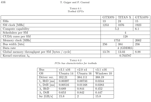
Table 6.1
Testbed GPUs
GTX970 TITAN X GTX1070
SMs 13 24 15
SM clock [MHz] 1253 1076 1923
Compute capability 5.2 6.1
Schedulers per SM 4
CUDA cores per SM 128
Memory clock [MHz] 1753 2002
Bus width [bits] 256 384 256
Data rate 4 (GDDR5)
Global memory throughput per SM [bytes / cycle] 13.78 13.03 8.88
Kernel executionλk 0.703787
Table 6.2
PCIe bus characteristics for testbeds
Bus v3.1 x16 v2.0 x4 v3.1 x16
OS Ubuntu 14 Ubuntu 16 Windows 10
Driver ver. 352.21 384.111 388.19
ts HtD [ms] 0.00397 0.00733 0.0244
ts DtH [ms] 0.00516 0.01168 0.0283
λc HtD 0.689 0.844 0.452
λc DtH 0.653 0.842 0.447
bw[GB/s] 15.8 2 15.8
addition to compute intensity, the third scenario concerned varying occupancy and the fourth changing input data size. In the first three scenarios, we measured only the kernel execution time as the data size was constant and memory copying could be omitted. In the last one, however, we included the measurements of the data transfer times in both directions, as well as the execution time of the entire application. All measurements in this section were repeated 10 times and then a mean value was used.
6.1. Testbed Environment. The tests were performed using three testbeds, one with GTX 970 and
PCIe v3.1 16x, the second withGTX TITAN X (Maxwell edition) and PCIe v2.0 4x, and the last one with
GTX 1070 andPCIe v3.1 16x. The first two were running Linux, and the last one Windows (see Table 6.2). The model was calibrated for the setup withGTX 970 and the kernel executionλkwas found to equal 0.703787, it also turned out that the value of λk did not change for the second GPU. This is expected behaviour since both devices are of the same architecture (compute capability), which proves the correctness of the model. We have also used the sameλkfor the third GPU, representing a newer architecture (Pascal). The results were still accurate, it is likely because both architectures do not differ much in terms of instruction types and latencies. The devices differ in number ofSMs, SM clock and in terms of memory system, with GTX TITAN X having wider memory bus, the differences and similarities are summarised in Table 6.1.
For interconnects we have measured data transfer startup time (ts) and PCIe bus utilisation (λc) separately for each transfer direction: host to device (HtD) anddevice to host (DtH), the results are shown in Table 6.2. The transfer is slightly more efficient in the former case. We have also observed that bus utilisation was lower on Windows, when compared to Linux. This was likely caused by additional overhead incurred by Windows Display Driver Model (WDDM) [10].
Listing 6
Source code of a simple CUDA application used for tests
v o i d simpleCUDAApp ( i n t c o m p u t e I n t e n s i t y , i n t b lockS z , i n t shMem , i n t N) { s t d : : v e c t o r <f l o a t > x (N) , y (N) ;
f l o a t ∗d_x , ∗d_y ;
s i z e _ t s i z e = N ∗ s i z e o f ( f l o a t ) ; cudaMalloc (&d_x , s i z e ) ;
cudaMalloc (&d_y , s i z e ) ;
cudaMemcpy (d_x , x . data ( ) , s i z e , cudaMemcpyHostToDevice ) ; cudaMemcpy (d_y , y . data ( ) , s i z e , cudaMemcpyHostToDevice ) ; i n t g r i d S z = (N+b lockS z−1)/ b l o c k S z ;
saxpy2<<<g r i d S z , b lockS z , shMem>>>(N, c o m p u t e I n t e n s i t y , d_x , d_y) ; cudaMemcpy ( y . data ( ) , d_y , s i z e , cudaMemcpyDeviceToHost ) ;
cudaFree (d_x) ; cudaFree (d_y) ; }
6.3. Tests and Results. In the first of the test scenarios we investigate the effect of a varying compute intensity of the kernel on its execution time. We have measured and simulated execution times for compute intensities (a parameter from Listing 2) spanning from 1 to 4096, while keeping all of the other parameters constant. This test verifies whether the theoretical model works for kernels exhibiting various ratios of com-putations to communication. For saxpy2 running with a maximum achievable occupancy of 64 warps per SM, if the intensity is low, then the kernel is bound by the throughput of a global memory, if it is high enough (32 in our case) it is bound by the CUDA cores throughput. We have observed that for all devices the model accurately determines the kernel execution time, however for lower compute intensities it is less precise, as the actual measured values diverge more from the predictions. This confirms that the model handles throughput bound scenario very well when the bound is imposed by the CUDA cores and is less accurate when it is due to the global memory system. The latter is not surprising as we have decided to take a simplified approach to the global memory modelling, by not considering the gradual saturation effect, using an equation to determine the theoretical memory throughput, and not adjusting it to the actual hardware characteristics.
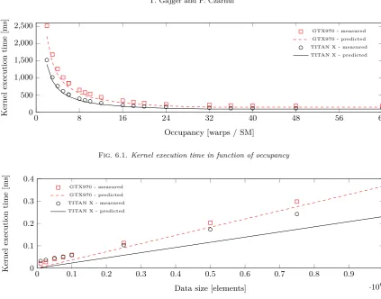
The second test case verifies whether our implementation of the model handles two performance modes -latency and throughput bound. To address both, we adjust the occupancy achieved when executing the kernel. To control the occupancy without modifying the block size we allocate dummy shared memory that effectively limits the maximum number of blocks that may be assigned to an SM. Note that it is not technically possible to cover every single value of the occupancy due to the fact how block and warp allocation works but nevertheless we were able to address a wide range of occupancies from 2 warps per SM to 64. Figure 6.1 shows the test results for Maxwell devices, the model precisely determines the kernel execution time with an average relative error of 5.4% and 7.8% forGTX 970 and GTX TITAN X respectively. ForGTX 1070 the error was 3.9%, we do not present it on this and subsequent figures for the sake of brevity. Furthermore, the transition from latency bound to throughput bound mode is represented accurately as well. Based on Fig. 6.1 we can determine the occupancy at which the transition occurs, this is around 32 warps / SM where rest of the figure becomes flat. However, for very small values of the occupancy the model overestimates the execution time by a small factor. Various block sizes were used when performing this test and it was noticed that the block size had no significant effect on the kernel execution time and the only significant factor was the occupancy. The validity of this conclusion is confirmed by the fact that what matters is the effectiveness of the utilisation of SM resources, which is directly related to achieved occupancy and not to the block size. The block size can only have an indirect effect by affecting the occupancy, which was not the case here once we excluded uncommon scenarios, where the size was smaller than 32. The proposed model is also based on calculation of the SM resources utilisation, therefore it behaved correctly in this scenario.
0 8 16 24 32 40 48 56 64 0
500 1
,000
1
,500
2,000
2
,500
Occupancy [warps / SM]
K
erne
l
ex
ec
ut
io
n
ti
m
e
[m
s]
GTX970 - measured
GTX970 - predicted
TITAN X - measured
TITAN X - predicted
Fig. 6.1.Kernel execution time in function of occupancy
0 0.1 0.2 0.3 0.4 0.5 0.6 0.7 0.8 0.9 1
·10 6 0
0
.1
0.2
0.3
0
.4
Data size [elements]
K
erne
l
ex
ec
ut
io
n
ti
m
e
[m
s]
GTX970 - measured
GTX970 - predicted
TITAN X - measured
TITAN X - predicted
Fig. 6.2.Kernel execution time for small data sizes
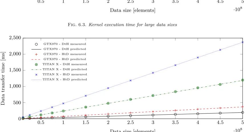
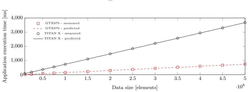
accurate when the data size is small and improves its accuracy as the number of elements to process increases. The average error for large data size was 3.7% (GTX 970), 4.6% (GTX TITAN X) and 13.6% (GTX 1070). The last one was expected to be higher since the model was calibrated for a different hardware architecture. The important fact is that even for the overestimated results, the functional relation between the data size and the execution time is maintained. This is acceptable since in real world scenarios the computations are performed for large data sizes and a case where the data is relatively small may be considered an uncommon one.
Since this test concerns a varying data size it must include data transfer time estimation, unlike the previous ones which focused only on the kernel execution. Given that our testbeds used different configurations of the PCIe bus we measuredλc andtsseparately for each of them. The results are presented in Table 6.2, these were then used as the parameters of the hardware unit, which are substituted to Eq. 4.6 in the computational model. Measured and estimated data transfer times are shown in Fig. 6.4. A decrease in accuracy for smaller data sizes resulting from an overestimation can be noticed, this is the same observation as in the case of the kernel execution time. Note that the transfers from host to the device take twice as much time because there are two arrays of N elements to be transferred in this direction, compared to only a single array that is transferred back. We have also proved experimentally here what was pointed out earlier, that the λc and ts assume different values depending on the transfer direction. If this effect was not considered, then the accuracy of the results would be lower. For large data sizes the predicted values very closely resemble the measured ones, thus we may conclude that the methodology proposed for measuring data transfer times is valid.
0
.5 1 1.5 2 2.5 3 3.5 4 4.5 5
·10 8 0
50 100 150 200
Data size [elements]
K
erne
l
ex
ec
ut
io
n
ti
m
e
[m
s]
GTX970 - measured
GTX970 - predicted
TITAN X - measured
TITAN X - predicted
Fig. 6.3. Kernel execution time for large data sizes
0.5 1 1.5 2 2.5 3 3.5 4 4.5 5
·10 8 0
500 1,000
1
,500
2,000
2
,500
Data size [elements]
Da
ta
tra
ns
fe
r
ti
m
e
[m
s]
GTX970 - DtH measured
GTX970 - DtH predicted
GTX970 - HtD measured
GTX970 - HtD predicted
TITAN X - DtH measured
TITAN X - DtH predicted
TITAN X - HtD measured
TITAN X - HtD predicted
Fig. 6.4.Data transfer times for large data sizes
prediction of the application execution time for the most essential scenario, achieving 1.8%, 0.5% and 1.5% mean relative error for large data size (≥10000000 elements, where 1 element = 8 Bytes as described in Section 5), for tested GPUs respectively. From the end user perspective, parameters like occupancy, block size and compute intensity will likely be determined once and then kept constant. What is probably the most common real-world use case, is verification of the application on different hardware setups and for different data sizes.
6.4. Discussion. For the most essential scenario with a varying data size, when this size was not very small, the mean values of the error were 1.8% forGTX 970 and 0.5% forGTX TITAN X. Tests of a compute bound kernel with varying occupancy yielded an average prediction error of 5.4% and 7.8% respectively which is also a very good result. When the input data size was small or the kernel was bound by a memory throughput, the relative prediction error had a mean value of 32.8% forGTX 970 and 9.9% forGTX TITAN X. Significantly worse results for a memory throughput bound kernel are caused by a highly simplified memory access model. For compute throughput bound kernels, the error went down to a few percent depending on the launch configuration. It should be further noted that for every test case the functional relationship between the launch configuration parameter being investigated and the application execution time was very closely reproduced by the model.
0
.5 1 1.5 2 2.5 3 3.5 4 4.5 5
·10 8 0
1
,000
2
,000
3,000
4,000
Data size [elements]
A
ppl
ic
a
ti
o
n
ex
ec
ut
io
n
ti
m
e
[m
s]
GTX970 - measured
GTX970 - predicted
TITAN X - measured
TITAN X - predicted
Fig. 6.5.Application execution times for large data sizes
shown that processing on a GPU may be conveniently modelled with a high degree of accuracy using a general-purpose simulator. MERPSYS, with the deployed model, allows its users to assess the behaviour of their applications for data sizes exceeding the hardware capabilities of units available to them and even use ones that are not in their possession, given that these are available in MERPSYS’ database. It allows to evaluate the application on hardware setups, on which testing prior to actual computational runs, would not otherwise be feasible, e.g. large clusters with a high cost per core-hour. It also allows to estimate the costs by predicting how long it will take for the computations to finish. In case of long-running applications, this allows for significantly shorter simulation times than the real runs.
The scope of modelling can be extended in the future as we have omitted double precision units, SFUs and shared memory, all of these could be fairly easy added to the model. Moreover, the approach to modelling of global memory accesses can be extended to consider caches, gradual saturation effect and varying access time depending on the transfer direction. So far we did include CUDA and NVIDIA GPUs in the model, possible extension includes its generalisation to be applicable to units produced by AMD and the OpenCL framework. The model can be extended with inclusion of an equation for occupancy calculation, which could be incorporated into the existing set of the equations and hence remove the need of relying on an external tool for this purpose. The solution would also largely benefit from an automation of the kernel analysis process. The behaviour of the model could also be verified on different GPU hardware architectures.
Acknowledgements. The work has been supported partially by the Polish Ministry of Science and Higher Education.
REFERENCES
[1] Top 500 list. [accessed November-2018].
[2] M. Amaris, D. Cordeiro, A. Goldman, and R. Y. d. Camargo, A simple bsp-based model to predict execution time
in gpu applications, in 2015 IEEE 22nd International Conference on High Performance Computing (HiPC), Dec 2015, pp. 285–294.
[3] M. Amaris, R. Y. de Camargo, M. Dyab, A. Goldman, and D. Trystram,A comparison of gpu execution time prediction
using machine learning and analytical modeling, in 2016 IEEE 15th International Symposium on Network Computing and Applications (NCA), Oct 2016, pp. 326–333.
[4] M. Andersch, J. Lucas, M. Alvarez-Mesa, and B. Juurlink,Analyzing gpgpu pipeline latency, in Proc. 10th Int. Summer
School on Advanced Computer Architecture and Compilation for High-Performance and Embedded Systems, Fiuggi, Italy (ACACES’ 14), July 2014.
[5] S. S. Baghsorkhi, M. Delahaye, S. J. Patel, W. D. Gropp, and W.-m. W. Hwu,An adaptive performance modeling
tool for gpu architectures, in Proceedings of the 15th ACM SIGPLAN Symposium on Principles and Practice of Parallel Programming, PPoPP ’10, New York, NY, USA, 2010, ACM, pp. 105–114.
[6] A. Bakhoda, G. L. Yuan, W. W. L. Fung, H. Wong, and T. M. Aamodt,Analyzing cuda workloads using a detailed