INTRODUCTION
In the recent past the structural and electrical studies of magnetic multilayers have been intensely pursued1. For example, [Ni(86Å)/ Fe(29Å)]11 multilayer was probed for texture and magnetic properties as a function of deposition temperature2. An irradiated multilayer, [Ni(13Å/ Fe(33Å)]10 with swift heavy ions was studied for magneto-optic Kerr effect and electrical resistivity as a function of temperature3. The interface mixing leading to alloy phase formation was observed when the films were irradiated. Similar studies were reported for Si+ ion irradiated Fe(28Å)/Ni(85Å) multilayers. Power laws for the resistivity variation with temperature were established. Experimental results on resistivity and magnetization in Ni-Fe alloy
Structural and Low Temperature Electrical
Properties of a Nickel/Iron multilayer
P.J. SADASHIVAIAH¹, T. SUJATHA², T. SANKARAPPA¹*,
SANTOSHKUMAR¹ and A.K.BHATNAGAR³
¹Department of Physics, Gulbarga University, Gulbarga - 585 106 (India). ²H.P.S. Kalkhora, Basavakalyan (Tq), Bidar (Dt) (India).
²School of Physics, Hyderabad University, Gachibowli, Hyderabad (India). *Corresponding author: E-mail: [email protected]
(Received: August 10, 2011; Accepted: September 17, 2011)
ABSTRACT
A multilayer, [Ni(100nm)/Fe(100nm)]5 has been deposited by electron beam evaporation method under high vacuum at 473 K. The structure and grain size were investigated by the grazing incidence X-ray diffraction (GIXRD) studies. The surface roughness was determined by atomic force microscope (AFM). Electrical resistivity has been measured in the temperature range from 4.2K to 300K. The resistivity increased with increase in temperature. The residual resistivity ratio (RRR) and the temperature coefficient of resistivity (TCR) were determined. The power law variations of resistivity with temperature were established. For temperature, T, above 80K, the resistivity exponent was found to be slightly more than unity and it was nearly 5 for temperature below 30K. The contributions to resistivity for T above 80K are attributed to be predominant by electron-phonon and electron-magnon scatterings and for below 30K they are ascribed to be predominant by electron-electron and electron-defect scattering.
Key words: Multilayers, Surface roughness, Resistivity, Residual resistivity ratio (RRR).
films are repor ted4. The Ni/Fe bilayers are technologically very important because of their low resistivity. From this brief literature survey, it can be understood that the detailed studies of structure and electrical properties have not been reported for Nickel/Iron multilayers. In view of this, we studied structural and electrical properties of a multilayer, [Ni/Fe]5.
EXPERIMENTAL
sources from two separate molybdenum crucibles using two independent electron beam guns. The thickness of the layers was measured with the help of quartz crystal thickness monitor. The films were annealed to room temperature slowly in the vacuum chamber.
Structural investigations were carried out by grazing incidence X- ray diffraction (GIXRD) studies using Brucker-D8 advance diffractometer with Cu-Kα radiation of 1.5406 Å wavelength. Surface morphology of the films was investigated by AFM (Digital Instruments Nanoscope III). Average grain size and surface roughness of the films were determined on a scan area of 1µm × 1µm using Nanoscope software. The low temperature (4.2K to 300K) resistivity, ρ has been measured by adopting four probe method using an Oxford Instruments make resistivity setup.
RESULTS AND DISCUSSION
Grazing incidence X-ray diffraction (GIXRD) studies
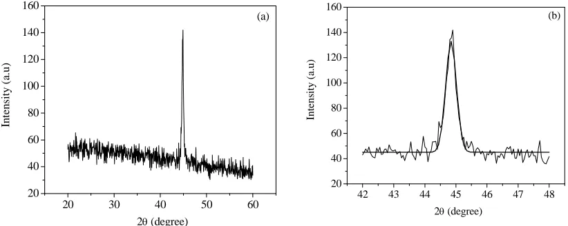
The GIXRD spectra for 2θ between 420 and 480 for the present film is shown in Fig.1(a) and the Gaussian fit to the peak is depicted in Fig.1(b). The spectra exhibited single sharp peak and its position does not exactly represent any plane in Fe or Ni crystals and therefore it can be considered to be representing a mixed phase (Ni(111)/Fe(110)) of Fe and Ni. No other peaks are visible in the
spectrum up to 600. The average grain sizes have been estimated using Scherrer’s formula [6],
(
0.9 /
cos
B)
D
=
λ
B
θ
, where, D is the grain size, B the angular width in terms of 2θ, θB the Bragg angle and λ the wavelength of X-rays. The interplanar spacing, d was calculated using the relation,(
/ 2 sin B)
d=
λ
θ
.The structure around the peak has been analyzed. The grain size and inter-planar spacing were determined to be 24.60 nm and 2.019 Å respectively.
AFM studies
The surface mor phology has been understood through AFM images which were recorded in contact mode with a scan area of 1ìm x 1ìm. The 2D and 3D AFM images of the film are shown in Fig. 2. The AFM image have been quantified by recording the height versus distance profile across the length (white line drawn in Fig. 2(a)) as shown in Fig.3 [7]. This analysis provided information about average grain size (D) (pair of blue dot lines in Fig.3) to be 118 nm and average surface roughness (h) (pair of red and green dot lines in Fig.3) to be 2.983 [8]. The grains appeared to be cubic in shape.
It can be noted that D value obtained from AFM studies is larger than that obtained from GIXRD. The disagreement between the grain sizes measured by two different methods could be due
20 30 40 50 60
20 40 60 80 100 120 140 160
In
te
n
sity
(
a.
u
)
2θ (degree)
(a)
42 43 44 45 46 47 48
20 40 60 80 100 120 140 160
Int
ens
it
y
(a.
u
)
2θ (degree)
(b)
Fig. 2: AFM images of the film (a) 2D (b) 3D
Fig. 3: Height, h versus Distance, D profile across the length white line drawn in Fig.2(a).
0 50 100 150 200 250 300
6 7 8 9 10 11
ρ
(1
0
-7 Ω
m)
T (K)
Fig. 4: Resistivity, ρρρρρ versus temperature, T plot for film for the complete temperature range
to the fact the measurements on AMF images are based on visual inspection. In case of GIXRD, it is to do with microscopic scattering of X-rays with lattice points/planes. This further reveals that the grains obser ved in AFM images are the agglomerates of many small crystallites that were seen by XRD. Such small crystallites in the images can be observed by High Resolution Transmission Electron Microscopy (HRTEM)9.
range from 5K to 300K. The room temperature (300K) ρ is greater by one to two orders of magnitude than the bulk ρ value of the two components (Ni ~ 0.072 µΩm and Fe ~ 0.09 µΩm). The larger ρ measured in this film may be due to intermixing of layers at the interface10 and this was also evident from GIXRD results.
The temperature coefficient of resistivity, TCR = (dρ/dT)/ρRT is determined to be 1.670 x 10⁻³ K-1. It may be noted that TCR has been determined for the temperature range from 80K to 300K, where ρ varied linearly with T. The positive TCR points to the metallic behavior of the film. The residual resistivity ratio, RRR is 1.67 and it is smaller than that expected for pure bulk metals. The small RRR value observed in this films may be due to enhanced electron-electron, interfacial, grain boundary etc., scatterings5,11.
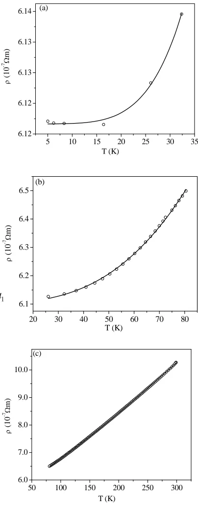
A close observation variation of ρ with T revealed that there exist three different power laws for the measured temperature range. Hence, the following expressions were fit to the data,
1
( )
T
(0)
a T
kρ
=
ρ
+
for T ≤ 30K2
( )
T
(0)
a T
mρ
=
ρ
+
for 30K ≤ T≤ 80K3
( )
T
(0)
a T
nρ
=
ρ
+
for 80K ≤ T ≤ 300Kwhere,
ρ
(0) is the residual resistivity which is taken to be equal to the measured value at 5K in all the films. By non linear curve fitting, the coefficients1
a
,
a
2anda
3 and exponents k, m and n were determined. The fit parameters thus obtained are = 0.911 µΩ m K-k, = 1.514 µΩm K-m, = 5.483 µΩm K-n, k = 4.76, m = 2.84 and n = 1.18. The data and the fit curves for the temperature range T ≤ 30K, 30K ≤ T ≤ 80K and 80K ≤ T ≤ 300K are shown in Fig.5(a-c).For pure nonmagnetic metals, the resistivity varies linearly with temperature (high temperature). For the present film, in the temperature range, 80K ≤ T ≤ 300K the coefficient, n is obtained to be slightly more than unity which
5 10 15 20 25 30 35
6.12 6.12 6.13 6.13 6.14
ρ
(10
-7 Ω
m)
T (K) (a)
20 30 40 50 60 70 80
6.1 6.2 6.3 6.4 6.5
ρ
(1
0
-7 Ω
m)
T (K) (b)
50 100 150 200 250 300
6.0 7.0 8.0 9.0 10.0
ρ
(1
0
-7 Ω
m)
T (K) (c)
Fig. 5: Resistivity, ρρρρρ versus temperature, T plots of (a) 5K to 30K, (b) 30K to 80K and (c) 80K to 300K for the film. The continuous curves passing through the data points are
reveals the predominance of electron-phonon scattering. In Fe/Ni multilayer, the resistivity was found to vary as T1.44 for the temperature range from 80K to 300K and this was attributed to additional electron-magnon (s-d) scattering, where s electrons were expected to scatter by magnons in to d band holes [3]. In the temperature range, 30K ≤ T ≤ 80K, the exponent, m is found to be 2.84 and that agrees with a magnetic layer [3] and deviates from White and Woods value of 3.3 for bulk Fe [13]. For the temperature, T ≤ 30K, the exponent, k is found to be 4.76. This result points out that in this range of temperature major contributions are from electron-electron and electron-electron-defects (which includes impurity) scatterings.
CONCLUSIONS
A Multilayer [Ni(100nm)/Fe(100nm)]5 has been investigated for structure, grain size and surface roughness through GIXRD and AFM.
Electrical resistivity as a function of temperature in the range from 4.2K to 300K has been measured. The residual resistance ratio (RRR) and the temperature coefficient of resistance (TCR) were deter mined. Resistivity increased with increasing temperature. The power laws for the resistivity variation with temperature were established. The power law exponent was slightly more than unity in the temperature region 80K≤ T≤300K and about 5 in the low temperature region T≤30K. It is concluded that in this film, electron-electron and electron-electron-defect scatterings are predominant below 30K and, electron-phonon and electron-magnon scatterings are predominant above 80K.
ACKNOWLEDGEMENTS
Authors also grateful acknowledge the experimental help received from Dr.R.Rawat, Scientist and Prof. Ajaya Gupta, Director of UGC-DAE consortium for Scientific Research, Indore, India.
1. B. Heinrich, S.T. Purcell, J.R. Dutcher, K.B. Urquhart, J.F. Cochran and A.S. Arrott, Phys. Rev. B 38: 12 879 (1988).
2. T. Veres, M. Cai, R. Morel, R. W. Cochrane, R. Abdouche and M. Sutton, J. Appl. Phys., 81: 4758 (1997).
3. S. K. Srivastava, Ravikumar, A. Gupta, R. S. Patel, A.K. Majumdar, D. K.Avasthi, Nuclear Instruments and Methods in Physics Research, B 243: 304 (2004).
4. Y.C. Yeh , C.W. Huang and J.T. Lue, Applied Surface Science, 254: 3420 (2008). 5. P.J.Sadashivaiah, T.Sankarappa, T.Sujatha,
Santoshkumar, R.Rawat, P.Saravanan and A.K.Bhatnagar, Vacuum, 85: 466 (2010). 6. B.D.Cullity: Elements of X-ray Diffraction
(Addison-Wesley Inc., Massachusetts, USA, 1956)
7. D. K. Aswal, K. P. Muthe, Shilpa Tawde, Sipra
REFERENCES
Chodhury, N. Bagkar, Ajay Singh, S. K. Gupta and J. V. Lakhmi, Journal of Crystal Growth, 236: 661 (2002).
8. B. Sasi and K. G. Gopchandran,
Nanotechnology, 18: 115613 (2007). 9. J. B. Yi, Y. Z. Zhou, J. Ding, G. M. Chow, Z. L.
Dong, T. White, Xing Yu Gao, A. T. S. Wee and X. J. Yu, J. Mag. Mag. Mater. 284: 303 (2004).
10. R. Brajpuriya, S. Tripathi, S. M. Chaudhari, Solid State Communication, 134: 479 (2005). 11. M. N. Ou, T. J. Yang, S. R. Harutyunyan, Y. Y. Chen, C. D. Chen, S. J. Lai, Appl. Phys. Letts. 92: 063101 (2008)
12. G.R. Taylor, A. Isin, R.E. Coleman, Phys. Rev. 165: 621 (1968).