A 0.7 V 0.0017 mV/V CMOS Voltage Reference with
No Amplifier
Yanfeng Bao
(Department of Electronic Engineering, JiNan University, Guangzhou 510632, China)
---
************************
---Abstract:
A low-supply voltage, high-power supply rejection ratio (PSRR), low-line sensitivity (LS) CMOS voltage reference with no amplifier is presented in this paper. The low LS is realized by the supply voltage independent bias currents. The circuit only consists of CMOS transistors and a resistor, which will decrease the supply voltage and area. The proposed voltage reference is designed in the standard 0.18 µm CMOS process. The simulation results show that the minimum power supply voltage is lower than 0.7 V. The temperature coefficient (TC) is 50 ppm/℃ to 56 ppm/℃ for a wide temperature range of -40℃ to
130℃, while the power consumption is 4.35 µW at 0.7 V. The simulated line sensitivity is 0.0017 mV/V
at room temperature. Under the TT process corner, the simulated PSRR is -91.5 dB at 1 KHz when the supply voltage is 0.7 V.
---
************************
---I. INTRODUCTION
As an essential building component in integrated circuits, voltage reference is widely used in A/D and D/A converters, phase locked loops [1] and so on. With the development of low power applications such as portable devices and wireless sensor networks [2, 3], low-voltage circuits have attracted considerable attention.
Voltagereferences[4-6] are implemented through Bipolar Junction Transistors (BJTs). However, since the turn-on voltage of the BJT is typically 0.7 V, a high power supply voltage is required. This does not meet the requirements of modern low voltage and low power consumption. In order to work out the problem, Yang et al. [7] exploit supply voltage boost to reduce power supply voltage, but charge-pump and digital control circuits increase the area and the power consumption.
There are no BJTs or boost circuits in [8-10], which use MOSFET-only to achieve low voltage and low power consumption. However, the current of the biasing circuits is so sensitive to the power supply voltage that it produces a very poor line
sensitivity (LS). Meanwhile, the junction leakage current may seriously affect the subthreshold characteristics of the MOSFETs[11], resulting in most nanowattsubthreshold voltage references only operate reliably over a limited temperature range. Therefore, high power consumption is required to obtain a wide temperature range and a low temperature coefficient (TC).
LS directly affects the power supply rejection ratio (PSRR) of the circuits, so it should be as small as possible [12]. To achieve a low LS voltage reference, amplifier is utilized in [13, 14] to increase the loop gain on the bias circuit. However, the amplifier consumes the voltage headroom. another method employs cascode stages [15], which increases the minimum supply voltage.
In this paper, in order to improve LS, we use negative feedback technique to obtain a current source which is independent of the voltage source.Through body-bias technique, a low TC voltage can be achieved.
International Journal of Computer Techniques -– Volume 6 Issue 1, Jan – Feb 2019
II.PRINCIPLE OF THE PROPOSED VOLTAGE REFERENCE
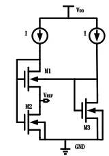
The principle of the voltage reference is shown in Fig. 1[9]. The voltage reference consists of current sources and three NMOS transistors operating in the subthreshold region. In such structure, when the MOSFET works in the sub-threshold region, the drain current ID of the MOSFET is given by [12]
(
)
η µ η − = − − − 21 exp 1 exp
GS TH T V V
V DS
D ox T
T V W
I C V
L V (1)
where µ is the carrier mobility, Cox is the gate-oxide capacitance, η is the sub-threshold slope factor,
W/L is the transistor aspect ratio, VT= KBT /q is the thermal voltage, KB is the Boltzmann constant, T is the absolute temperature, q is the elementary charge, and VTH is the threshold voltage of the MOSFET,
VGS and VDS are the gate-source voltage and drain-source voltage of the MOSFET, respectively. For
VDS≥ 4VT, the current ID is independent of VDS,thus the gate-source voltage of M3 can be approximated by
(
)
η µ η = + − , 3 , 3
2
3
ln .
1
GS M TH M T
ox T
M I
V V V
W
C V
L
(2)
Since there is a body effect in M1, the threshold voltage of M1 can be expressed as [16, 17]
(
)
(
)
γ φ φ η = + + − ≈ + − 0 0 2 2 1TH TH F SB F
TH SB
V V V
V V (3)
whereVTH0 is the threshold voltage with zero body bias, γ is the body effect constant, ΦF is the Fermi potential and VSB is the source-bulk voltage of M1.
Then, using (2) and (3), reference voltage VREF can be acquired as
(
)
γ φ φ η
= −
= − + − +
, 2 , 1
1 , 3
2
2 2 ln
REF GS M GS M
M
F F REF GS M T
M
V V V
K
V V V
K
(4)
whereKM1 and KM2 are the aspect ratios of M1 and M2, respectively.
Furthermore, (4) can be rearranged as
(
)
′
= ∆ + , 3
REF GS GS M
V V f V (5)
where∆VGS′ =ηVTln
(
KM1 KM2)
,(
)
(
(
)
)
(
)
(
)
(
1 2)
, 3, 3
4 2 2 ln .
2 2 2
γ γ γ φ φ η
γ γ φ
− + + + −
= +
F F T M M GS M
F GS M
V K K V
f V
In view of the fact that the current source I is related to VDD, we have
(
)
(
)
2
, 3 3
2 3 1 1 1 . µ η η µ η η ∂ − ∂ = ∂ ∂ × − ∂ = ∂
GS M n ox M T
T
DD DD
n ox M T
T
DD
V C K V I
V
V I V
C K V
V I
I V
(6)
The PSRR can be evaluated by taking the derivative of (5) with respect to VDD and inserting (6) , 3 1 , 3 2 1 , 3 2 2 ( 2 ) 2 ln
4
.
2 ( 2 ) 2 ln 4 γ γ γ φ φ η η γ γ γ φ φ η ∂ − ∂ ∂ = − ∂ + + + − ∂ ∂ = + + + − GS M REF DD DD M
F F T GS M
M
T DD
M
F F T GS M
M V V V V K V V K I V V I K V V K (7)
From (7), we can find that the PSRR of the circuit mainly depends on the variation of I with
VDD. Therefore, in order to achieve high PSRR and low LS, a current source that is independent of the power supply should be considered.
[18] utilizes the difference in gate-source voltage of MOS transistors across the resistor R
the circuit is very sensitive to the supply voltage variations. So all of these current generators result in poor LS.
To obtain a current generator which is independent ofVDD, we use negative feedback technique [19] without amplifier and cascade stages.
I II
I IIII
M M M M 1111
M M M M 2222
M M M M 3333 V V V VREFREFREFREF
V VV VD DD DD DD D
GND GND GND GND
Fig. 1Principle of the voltage reference
The schematic of the proposed voltage reference is illustrated in Fig.2. The circuit consists of start-up circuit, current generator, output stage and body bias circuit. The start-up circuit helps the circuit get rid of the degeneracy point and enter the second steady state. TheMOSFETs MP1-MP5are operated in the saturation region, and MN1-MN5 work in the subthreshold region. Main section will be described in the following.
Fig. 2Schematic of the proposed voltage reference
A. Current Generator
In the current generator, the negative feedback loop is composed of MN2, MN1, MP1, and MP3. Therefore, when the node voltage C rises with the power supply variation, the voltage of the node B drops, and then the node A rises. Since the negative feedback is greater than the positive feedback formed by MN1, MP1, MP2, the node C falls at last, and vice versa. In this way, it is guaranteed that the
current flowing through the resistor R remains constant.
From Fig. 2. VGS,MN2is the voltage acrossR.The current flowing through R can be described as IR =
VGS,MN2 /R. Due to (W/L)MP1 = (W/L)MP2 = (W/L)MP3, we can get that the current flowing through R is approximately equal to the currents of transistor MN2 and MN1. The temperature dependence of threshold voltage can be expressed as [10]
(
)
δ
= 0− − 0 TH TH
V V T T (8)
whereT0 is the reference temperature, δ is the threshold temperature exponent. The nonlinear temperature dependence of mobility is µ(T) =
µ(T0)(T/T0)-α, where µ(T0) is the carrier mobility at temperature T0, α is the mobility temperature exponent about 1.5-2 [20].
Since VGS decreases with temperature for any fixed drain current ID,we can approximate write
as [21]
( )
0 0
GS GS
V =V −β T−T (9)
whereβ is positive quantity, VGS0 is the gate-source voltage at the temperature T0.
Therefore, for VDS ≥ 4VT, substituting the expressions (8) and (9) into (1), the expression of current flowing through MN2 can be got
(
)
(
)
µ η
δ β
η η
= − ⋅
−
⋅
2 2
, 2 0 0 2
2
( ) 1
exp exp .
B
D MN ox
MN
B
K W
I T T C
L q
q m
K T
(10)
International Journal of Computer Techniques -– Volume 6 Issue 1, Jan – Feb 2019
Fig. 3Small-signal equivalent model of the current generator
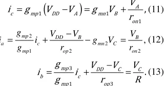
Fig. 3 shows the small signal model of the current generator. From Fig. 3, we can get the following expression according to Kirchhoff's current law
(
)
= 1 − = 1 +
1 , A c mp DD A mn B
on V
i g V V g V
r (11) 2
2
1 2 2
,
mp DD B B
a c mn C
mp op on
g V V V
i i g V
g r r
−
= + − = (12)
−
= 3 + =
1 3
.
mp DD C C
b c
mp op
g V V V
i i
g r R (13)
Through simultaneous equations (11)-(13), the relationship between ic and VDD can be expressed as
≈
− +
+ − +
1 1 3 1 1 2 2
3 2 1
1 2 2 3 3 2 3
2 2
(14)
.
( )
( ( ))
/ /
c
DD
mp mn op mp mn op mn
op op mp
mn op mn mp op mp op op on
i V
g g r g g r g R
R r r g
g r g g r R g R r
r r
wheregmni represents the transconductance of MNi,
gmpi represents the transconductance of MPi, roni represents the output resistance of MNi,
ropirepresents the output resistance of MPi. From Expression (14), it is obvious that the sensitivity of
ic to VDD is proportional to R and gmn2. Consequently, the sizes of the resistor R and the transistor MN2 are appropriately adjusted to obtain a current source independent of VDD. The current of the current generator is mirrored to the output stage through transistor MP4. As shown in Fig. 4, the current IMN3 of the output stage changes only 171 pAwhen the supply voltage changes 1.1 V.
Fig. 4 Simulated current of IMN3 versus supply voltage
B. Output Stage
The output stage circuit is formed by MN3 and MN4 operating in the subthreshold region. With the body-bias technique, the threshold voltages of MN3 and MN4 are different. In this way, a low TC VREF is obtained. Since the source-bulk voltage of MN3 is not zero, the body effect exists. Therefore, using the same derivation method used in expression (6) in Section 2, reference voltage VREFbecomes
(
)
′
= ∆ + , 5
REF GS GS MN
V V f V (15)
where∆VGS′ =ηVTln
(
KMN3 KMN4)
,(
)
(
(
)
)
(
)
(
)
(
3 4)
, 5, 5
4 2 2 ln ,
2 2 2
γ γ γ φ φ η
γ γ φ
− + + + −
= +
F F T MN MN GS MN
F GS MN
V K K V
f V
(
)
(
)
(
)
, 2
, 5 , 5 2
0 5
2
0 0 0 , 5
5
ln
( ) 1
ln
D MN GS MN TH MN T
ox MN T
MN
T GS TH TH MN
MN
bI
V V V
T C K V
bK
V T V V T V
K
η
µ η
η δ β β δ
= +
−
= + − + − + − +
where b=KMP5/KMP2, and KMP2, KMN3, KMN4, KMN5,
KMP5 are the aspect ratios of MP2, MN3, MN4, MN5, and MP5, respectively. ∆VGS′ is the gate-source
voltage difference between MN3 and MN4 when the substrate of MN3 is connected to ground and has a positive TC. VGS,MN5 and f(VGS,MN5) are a negative TC voltage because the slope of VTH,MN5 is larger than that of VT. The two opposite TC voltages (∆VGS′ , f(V
By Simplifying (15), the output voltage be got as
REF
V =A+BT−γ C+BT−DT−E
whereA=
(
γ γ(
+2 2φF)
2 ,)
ln ,B K
K B
q K
η
=
(
)
(
4 2 F)
2 F,C=γ γ + φ + φ 5 2 2 5 ln MP MN ,
B
MP MN
K K K
D
q K K
η β
= −
0 GS0,MN2. E=βT +V
According to (16), the first derivative of with temperature can be expressed as
(
2
REF
V B D
B
T γ C B D T E
∂ −
= −
∂ + − −
Let ∂VREF/∂T = 0, we can get
(
2 2
4
B D
T
B
γ −
= +
By adjusting the KMN3-KMN5 properly, we can get a low TC voltage reference over a wide temperature range.
III. SIMULATION RESULTS
Based on TSMC 0.18 µm CMOS process, the pre-simulations and post layout simulations of proposed voltage reference have been finished. Fig. 5 shows the layout of the proposed voltage reference. The total layout area is 0.0067 mm
Fig. 5 Layout of proposed voltage reference
Fig. 6 shows the simulation results of the reference voltage versus temperature in the range of Simplifying (15), the output voltage VREF can
V =A+BT− C+BT−DT−E(16)
3
4 ln MN ,
MN
K q K
5 2
2 5 ln MP MN ,
MP MN
K K q K K
η β
= −
According to (16), the first derivative of VREF
)
.B D
C B D T E
−
+ − − (17)
)
.
B D E C
B D
−
= +
− (18)
properly, we can get a low TC voltage reference over a wide temperature
m CMOS process, the simulations and post layout simulations of voltage reference have been finished. Fig. 5 shows the layout of the proposed voltage reference. The total layout area is 0.0067 mm2.
Layout of proposed voltage reference
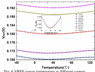
Fig. 6 shows the simulation results of the ature in the range of
-40℃to 130℃ at different process corners. It is
worth noting that the reference voltage has the same trend with temperature at different process corners. As described in Section 2, a low TC is achieved. We can get that the best TC is 50
process corner, and the worst TC is 56
SS process corner. The inset of Fig. 6 is the comparing between the pre-simulation and the post simulation at the TT process corner, we can find that the difference between the pre
post simulation results is very small, so the design of circuit is reasonable.
Fig. 6 VREF versus temperature at different corners
Fig. 7 shows the simulated PSRR at different process corners when VDD is 0.7 V. The highest PSRR is -101.5 dB at 1 KHz when process corner is FF. The worst PSRR is -82.6 dB at 1 KHz when process corner is SS. As mentioned earlier, through the negative feedback technique, the variation of current source with power supply vol
small (see Fig. 4). Therefore, Fig. 7 shows the result of (7), we can find that a high PSRR is obtained at different process corners. The inset of Fig. 7 shows the PSRR at FS Pre and FF Pre, respectively
Fig. 7 Simulated PSRR versus frequency at different corners
at different process corners. It is worth noting that the reference voltage has the same trend with temperature at different process corners. As described in Section 2, a low TC is achieved. best TC is 50 ppm/℃ at FS
process corner, and the worst TC is 56 ppm/℃ at
The inset of Fig. 6 is the simulation and the post-simulation at the TT process corner, we can find that the difference between the pre-simulation and post simulation results is very small, so the design
VREF versus temperature at different corners
Fig. 7 shows the simulated PSRR at different is 0.7 V. The highest 101.5 dB at 1 KHz when process corner is 82.6 dB at 1 KHz when process corner is SS. As mentioned earlier, through the negative feedback technique, the variation of current source with power supply voltage is very small (see Fig. 4). Therefore, Fig. 7 shows the result of (7), we can find that a high PSRR is obtained at different process corners. The inset of Fig. 7 shows the PSRR at FS Pre and FF Pre, respectively.
International Journal of Computer Techniques -– Volume 6 Issue 1, Jan – Feb 2019
The relationship between PSRR andfrequency under different supply voltages is presented in Fig. 8. We can see that an excellent PSRR is also exhibited at different supply voltages. For the supply voltage of 0.7 V, the simulated PSRR reaches -91.5 dB at 10 KHz. the simulated PSRR can reach -111.2 dB at 10 KHz when the supply voltage is 0.9 V.
Fig. 8 Simulated PSRR versus frequency at different power supply
The LS is defined as LS= (∆VREF/∆VDD). It can be found from (7) that LS and PSRR are related. When the LS is lower, a high PSRR can be implemented. So using negative feedback, we not only get an excellent PSRR but also obtain a low LS. As shown in Fig. 9, when the simulated supply voltage sweeps from 0.7 V to 1.8 V, the voltage reference only changes 1.9 µV at TT process corner. Consequently, the LS can be calculated to be 0.0017 mV/V.
Fig. 9 Simulated Line regulation at different supply voltage.
To guarantee correct function of the circuit against process variation and mismatch, Monte Carlo simulation is performed on 100 samples at
room temperature and typical process corner, as shown in Fig. 10. It can be found that the mean valueu of VREF is 179.69 mV, the standard deviation σ is 3.64 mV. So the coefficient of variation (σ/u) is about 2.0%. By properly setting the size of the transistor and making the current mirrors MP1-MP5 operate in the saturation region, process variations and mismatches can be diminished.
Fig. 10 Monte-Carlo Simulation result of reference voltage
The overall performance is compared between the proposed voltage reference and other voltage references. The results are showed in Table 1. The proposed circuit, Ref [10] and Ref [14] are based on simulation results, while Ref [9] is the measurement result. It can be noticed that the proposedreference has an excellent PSRR and low LS due to the negative feedback technique. Owing to no special device, voltage reference in this paper has a wider application.
IV. CONCLUSIONS
A 0.7 V 0.0017 mV/V CMOS voltage reference without amplifier is designed in the standard 0.18 µm CMOS process. Low LS and high PSRR are achieved by using negative feedback technique. At
VDD = 0.7 V, the simulated PSRR up to -91.5 dB at 10 KHz. Most of transistors operate in the subthreshold region, which reduce supply voltage and power consumption. Through body-bias technique, the TC of the reference voltage is improved. The proposed low-supply voltage high-PSRR low-LR voltage reference can be attractive in the low-power battery-operated electronic applications.
REFERENCES
[1] Andreou, C.M., Koudounas, S., Georgiou, J.: ‘A novel wide-temperature-range, 3.9 ppm/℃ CMOS bandgapreference circuit’, IEEE
J. Solid-State Circuits., 2012, 47, (2), pp. 574-581
[2] Luo, S.C., Chiou, L.Y.: ‘A sub-200-mV voltage-scalable SRAM withtolerance of access failure by self-activated bitline sensing’, IEEE Trans.Circuits Syst. II, Express Briefs, 2010, 57, (6), pp. 440-445 [3] Papotto, G., Carrara, F., Finocchiaro, A., et al.: ‘A 90-nmCMOS
5-Mbps crystal-less RF-powered transceiver for wireless sensornetwork nodes’, IEEE J. Solid-State Circuits., 2014, 49, (2), pp. 335-346 [4] Zhou, Z., et al.: ‘A 1.6-V 25-µA 5-ppm/℃ curvature-compensated
bandgap reference,’ IEEE Trans. Circuits Syst.1.Reg.Papers, 2012, 59, (4), pp. 677-684
[5] Jinghu, L., Xingbao, Z., Mingyan, Y.: ‘A 1.2-V piecewise curvature-corrected bandgap reference in 0.5 m CMOS process’, IEEE Transactions on Very Large Scale Integration (VLSI) Systems, 2011, 19, (6), pp. 1118-1122
[6] Qingli, L., Wanling, D., Xiaoyu, M., et al.: ‘A novel low line regulation voltage reference with no amplifier’, Journal of Circuits, Systems, and Computers, 2018, 27, (10).
[7] Yang, B.D.: ‘250-mV supply subthreshold CMOS voltage reference usinga low-voltage comparator and a charge-pump circuit’, IEEE Trans. Circuits Syst. II, Express Briefs, 2014, 61, (11), pp. 850-854
[8] Magnelli, L., Crupi, F., Corsonello, P., et al.: ‘A 2.6 nW, 0.45 V temperature-compensated subthreshold CMOS voltage reference’, IEEE J. Solid-State Circuits., 2011, 46, (2), pp. 465-474
[9] Yutao, W., Zhangming, Z., Jiaojiao, Z., et al.: ‘A 0.45-V, 14.6-nW CMOS subthreshold voltage reference with no resistors and no BJTs’, IEEE Trans. Circuits Syst. II, Express Briefs, 2015, 62, (7), pp. 621-625
[10] Yuhua, L., Zhangming. Z.: ‘A 0.6 V 31 nW 25 ppm/°C MOSFET-only sub-threshold voltage reference’, Microelectronics Journal, 2017, 66, pp. 25-30
[11] Jize, J., Wei, S., JosephS, C.: ‘A 5.6 ppm/°C Temperature Coefficient,87-dB PSRR, Sub-1-V Voltage Referencein 65-nm CMOS Exploiting the Zero-Temperature-Coefficient Point’, IEEE J. Solid-State Circuits., 2017, 52, (3), pp. 623-633
[12] Zhangming, Z., Jin, H., Yutao, W.: ‘ A 0.45 V, Nano-Watt 0.033% Line Sensitivity MOSFET-Only Sub-Threshold Voltage Reference With no Amplifiers’, IEEE Transactions on Circuits and Systems, I, Regular Papers, 2016, 63, (9), pp. 1370-1380
[13] Yanhan, Z., Yirong, H., Yunling, L., et al.: ‘An ultra-low-power CMOS voltage reference generator based on body bias technique’, Microelectronics Journal, 2013, 44, (12), pp. 1145-1153
[14] Caicedo, J.A.G., Mattia, O.E., Klimach, H., et al.: ‘0.75 V supply nanowattresistorless sub-bandgap curvature compensated CMOS voltage reference ’, Analog IntegrCirc Sig Process, 2016, 88, (2), pp. 333-345
[15] Yuanming, Z., Fei, L., Yajuan, Y.: ‘A -115 dB PSRR CMOS bandgapreference with a novel voltage self-regulating technique’, Proc. Int.
Conf. CICC, San Jose, CA, USA, Sept 2014, pp. 1-4
[16] Allen, P.E., Holberg, D.R.: ‘CMOS analog circuit design’ (Oxford UniversityPress, USA, 2002)
[17] Luo, H., Han, Y., Cheung, R.C.C., et al.: ‘SubthresholdCMOS voltage reference circuit with body bias compensation for processvariation’, IET Circuits Devices Syst., 2012, 6, (3), pp. 198–203
[18] Ka Nang, L., Philip K. T, Mok.: ‘A CMOS voltage reference based on weighted △VGS for CMOS low-dropout linear regulators’, IEEE J. Solid-State Circuits., 2003, 38, (1), pp. 146-150
[19] Dong, Z., Allen, P.E.: ‘Low-voltage, supply independent CMOS bias circuit’, Proc. Int. Conf. IEEE Circuits and Systems, Tulsa, OK, USA, Aug 2002, pp. 568-570
[20] Zekun, Z., Peisheng, Z., et al.: ‘A CMOS Voltage Reference Based on Mutual Compensation of Vtn and Vtp’, IEEE Trans. Circuits Syst. II, Express Briefs, 2012, 59, (6), pp. 341-345
[21] Giustolisi, G., Palumbo, G., Criscione, M., et al.: ‘A Low-Voltage Low-Power Voltage Reference Based on Subthreshold MOSFETs’, IEEE Journal of solid-state circuits, 2003, 38, (1), pp. 151-154
Parameter Proposed Ref[9] Ref[10] Ref[14] Unit
Year 2018 2015 2017 2016
CMOS Technology 0.18µm 0.18µm 0.18µm 0.18µm -
Supply voltage 0.7 0.45 0.6 0.75 V
VREF 180 118.46 441 469 mV
Temperature Coefficient 52 63.6 25 18 ppm/
Temperature range -40-130 -40-125 -20-80 -40-125
σ/µ (Monte Carlo) 2.0 0.6 6.6 2.2 -
PSRR -91.5 -44.2 -44 -67 dB
Line regulation 0.0017 1.2 30 0.14 mV/V
Area 0.0067 0.012 0.0071 0.0053 mm2
![Fig. 1[9]. The voltage reference consists of current The principle of the voltage reference is shown in sources and three NMOS transistors operating in the subthreshold region](https://thumb-us.123doks.com/thumbv2/123dok_us/8800027.1771351/2.612.318.541.311.423/voltage-reference-consists-principle-reference-transistors-operating-subthreshold.webp)