PhD Dissertation
International Doctorate School in Information and
Communication Technologies
DISI - University of Trento
M
ODELING,
D
ESIGN ANDC
HARACTERIZATION OF AM
ULTI-P
IXELD
IGITALS
IPM
FORPET
APPLICATIONSLeo Huf Campos Braga
Advisor:
Dr. David Stoppa
Abstract
Positron Emission Tomography (PET) scanners provide functional three-dimensional images of the body that are extremely useful in cancer and brain research. The goal of this work is the modeling, design and characterization of a CMOS-based photodetector for PET. To this aim, first a model for the energy resolution and coincidence resolution time (CRT) for digital, SPAD-based detectors is developed.
Then, a top-to-bottom detector architecture is proposed, containing an innovative in-pixel com-pression technique that allows for high fill-factor (FF) and efficient readout. At the top-level of the architecture, an integrated discriminator monitors the photon flux for incoming gamma events, enabling an event-based readout scheme. The first complete implementation of this archi-tecture is described, the SPADnet-I sensor, which is composed by an 8×16 pixel array, each of around 0.6 × 0.6 mm2 with 720 SPADs, resulting in a pixel FF of 42.6%. The sensor can obtain the discrete photon flux estimation at up to 100 Msamples/s, which are used by the discriminator and also output at real-time.
The complete characterization of the sensor is presented, and the best sensor configuration was found to be at 84% of the SPADs enabled (disabled starting with the highest DCR one), with 2 V SPAD excess bias and 150 ns integration time. This configuration results in an energy resolution of 10.8% and a CRT of 288 ps, the latter which was obtained with a new, hardware-friendly time of arrival (ToA) estimation algorithm, also described in this thesis.
Finally, the sensor model, validated by the experimental results, is used to predict the perfor-mance of possible modifications in the sensor, and some design improvements are suggested for a future implementation of the architecture.
Keywords
Acknowledgements
First of all, I would like to thank my advisor David Stoppa for welcoming me into his research group in 2010 and guiding me throughout all these years. Without his experienced and intelligent technical and personal support I could not have achieved my goals.
I would also like to thank all research personnel at the SOI group, namely Matteo Perenzoni, Ni-cola Massari, Leonardo Gasparini, Lucio Pancheri, Daniele Perenzoni and Massimo Gottardi for their everyday advices and helpful discussions.
My colleagues at the research group SRS are also recipients of my truest appreciation, you were also instrumental in the success of my work. I personally name Claudio Piemonte, Alberto Gola, Nicola Serra, Alessandro Tarolli, Alessandro Ferri, Nicola Fronza and Gabrielle Giacomini for their support.
All partners in the SPADnet project were also fundamental in the completion of my PhD work. I wish to specifically acknowledge Robert Henderson and Richard Walker from the University of Edinburgh for their close cooperation in the design of the SPADnet-I sensor; Gabor Nemeth and Peter Major from MEDISO for sharing their abundant knowledge about PET systems; and again Richard Walker, Leonardo Gasparini and Zoltan Papp for the development of the firmware for the sensor characterization.
I express my gratitude also to Prof. Gian-Franco Dalla Betta from the University of Trento, for his help in all things related to the PhD, from constructive work goals to everyday problem solv-ing.
Many thanks also to my PhD colleagues, Elisabetta Mazzuca, Michelle Benetti, Marina Repich and Hesong Xu, with whom I could share the troubles (and occasional joys) of doing a PhD.
Contents
CHAPTER 1 INTRODUCTION ... 1
1.1. POSITRON EMISSION TOMOGRAPHY ... 1
1.2. THE PROPOSED SOLUTION... 4
1.3. STRUCTURE OF THE THESIS ... 5
CHAPTER 2 STATE OF THE ART ... 7
2.1. SILICON PHOTOMULTIPLIERS ... 7
CHAPTER 3 GAMMA DETECTION IN PET SCANNERS ... 12
3.1. GAMMA DISCRIMINATION ... 12
3.2. ENERGY ESTIMATION ... 14
3.3. TIME OF ARRIVAL ESTIMATION ... 18
3.3.1 Timestamp Model ... 19
3.3.2 Methods for Timing Resolution Assessment ... 23
3.3.3 Analysis ... 25
3.4. POSITION ESTIMATION ... 30
3.5. OTHER FEATURES ... 33
3.6. SUMMARY ... 34
CHAPTER 4 THE SPADNET SENSOR ... 36
4.1. SPAD-BASED SENSORS: DESIGN CONCEPTS AND COMPROMISES... 36
4.2. SENSOR ARCHITECTURE ... 39
4.2.1 Counting photons: the mini-SiPM ... 39
4.2.2 Gamma detection: the top-level ... 44
4.2.4 Timing Diagram ... 49
4.3. FIRST IMPLEMENTATION: SPADNET-I ... 51
4.3.1 Hierarchy sizing ... 51
4.3.2 Schematics ... 55
4.3.3 Layout floorplans ... 59
4.3.4 Chip micrograph ... 62
CHAPTER 5 PROCESSING SPADNET DATA ... 65
5.1. ENERGY ... 65
5.2. TIME OF ARRIVAL ... 68
5.2.1 From codes to timestamps ... 68
5.2.2 Finding the first photon ... 70
5.2.3 ToA Estimators ... 72
CHAPTER 6 EXPERIMENTAL RESULTS ... 78
6.1. ELECTRO-OPTICAL CHARACTERIZATION ... 79
6.1.1 Monostable pulse width ... 79
6.1.2 TDC linearity and resolution ... 80
6.1.3 SPAD DCR and timing resolution ... 82
6.1.4 Pixel jitter and skew ... 83
6.2. SCINTILLATION CHARACTERIZATION ... 86
6.2.1 System functionality... 87
6.2.2 Performance optimization ... 93
6.2.3 Suggested sensor configuration results ... 100
CHAPTER 7 CONCLUSIONS... 104
7.1. FUTURE WORK ... 106
List of Tables
List of Figures
Figure 1: PET working principle. ... 2 Figure 2: Scintillation light pulse hitting the photosensor and its respective outputs. ... 3 Figure 3: analog (a) and digital (b) SiPM architectures. ... 8 Figure 4: expected flux (photon and noise) at the photosensor when an event occurs at time Θ. 13 Figure 5: expected counting output based on the flux of Figure 4, for a gamma event arriving at two different times, Θ1 and Θ2. ... 14
Figure 17: CRT of the Cramér-Rao bound considering the complete model (photon emission, jitter and noise) versus the number of detected photons and the noise rate, with a fixed jitter
FWHM of 150 ps. ... 30
Figure 18: operation principle of SPADs in CMOS technology. ... 37
Figure 19: energy resolution versus SPAD active diameter for round SPADs based on [Ric+11]. Detection of 1000 and 1500 photons is assumed in an area containing 50k SPADs with 15 μm active diameter. ... 38
Figure 20: sensor hierarchy overview. ... 39
Figure 21: simplified schematic of the mini-SiPM architecture, highlighting the two compression schemes: spatial and temporal. ... 40
Figure 22: example of a mini-SiPM with 32 SPADs and a timing diagram. ... 43
Figure 23: examples of mini-SiPM floorplans with (a) round and (b) square SPADs. ... 43
Figure 24: block diagram of the sensor top-level. ... 45
Figure 25: state diagram of the discriminator. ... 45
Figure 26: block diagram of the pixel, also showing the required modifications at the mini-SiPM. ... 47
Figure 27: average probability of the TDC being triggered by a dark count before a gamma event arrives. ... 49
Figure 28: timing diagram of the sensor. ... 50
Figure 29: spatial compression loss estimation versus number of SPADs. ... 52
Figure 30: temporal compression loss estimation versus number of SPADs. ... 53
Figure 31: mini-SiPM schematics. ... 55
Figure 32: pixel schematics. ... 56
Figure 33: TDC block diagram. ... 57
Figure 36: mini-SiPM electronics floorplan... 59
Figure 37: pixel floorplan. ... 60
Figure 38: floorplan of the first three levels of the adder tree. ... 61
Figure 39: floorplan of the last four levels of the adder tree. ... 61
Figure 40: SPADnet-I micrograph. ... 62
Figure 41: SPADnet-I chip with backside ball grid array. ... 63
Figure 42: example of SPADnet-I fitted response curve (compression curve). ... 67
Figure 43: raw count spectrum used to obtain the data points in Figure 42 and the resulting gamma energy spectrum. ... 67
Figure 44: example of a 3-bit TDC response and its possible fits. ... 69
Figure 45: cumulative distribution of timestamps obtained from a typical gamma event, with a rough indication of the gamma ToA. ... 70
Figure 46: intervals between the timestamps shown in Figure 45. ... 71
Figure 47: coincidence time distribution using the first photon as the gamma ToA, for three different parameter combinations of the first photon finder algorithm. ... 72
Figure 48: illustration of estimator steps with a typical Monte Carlo simulation-generated data: (a) comparison of expected and simulated CDF; (b) difference vector between the two. ... 75
Figure 49: Monte Carlo simulation results comparing the CRT of single-timestamp estimators with the proposed multiple-timestamp estimators. ... 76
Figure 50: sensor characterization assembly. ... 78
Figure 51: monostable pulse width versus control voltage. ... 79
Figure 52: TDC characterization: (a) histogram of all TDCs LSB resolution; (b) and (c) minimum, maximum and typical DNL and INL values, respectively. ... 81
Figure 54: SPAD-only timing resolution for different excess bias voltages: (a) histogram of
timestamps; (b) obtained FWHM versus excess bias. ... 83
Figure 55: jitter of a typical pixel for different SPAD excess bias voltages: (a) histogram of timestamps; (b) obtained FWHM versus excess bias. ... 84
Figure 56: histogram of all pixels jitter FWHM. ... 85
Figure 57: map of pixel skew (a) and jitter FWHM (b) at 3 V SPAD excess bias. ... 85
Figure 58: setup for gamma coincidence measurements. ... 86
Figure 59: examples of typical 511 keV, 1275 keV and pile-up events: (a)-(c) real-time energy output and (d)-(f) pixel counts. ... 87
Figure 60: pixel maps averaged for 75k events with energy around 511 keV: (a) pixel counts and (b) TDC triggering probability. ... 88
Figure 61: total sensor counts histogram for different discriminator thresholds. ... 89
Figure 62: measured distribution in time of 511 keV gamma events. ... 90
Figure 63: spatial and temporal compression loss assessment. ... 92
Figure 64: parameters of the sensor response fits for different SPAD excess bias and number of SPADs enabled: (a) k; (b) DC. Highest DCR SPADs disabled first. ... 94
Figure 65: DC of the sensor response equation fits for different SPAD excess bias and number of SPADs enabled. Lowest DCR SPADs disabled first. ... 95
Figure 66: energy resolution for different SPAD excess bias and number of SPADs enabled, with highest DCR SPADs disabled first. ... 96
Figure 67: energy resolution versus number of SPADs enabled at 2 V SPAD excess bias, with two sorting orders for disabling the SPADs: highest DCR first and lowest DCR first. ... 97
Figure 68: CRT versus number of SPADs enabled at 2 V SPAD excess bias, with highest DCR SPADs disabled first. ... 98
List of PhD Publications
Patent applications
1. L. H. C. Braga, M. Perenzoni, N. Massari, L. Gasparini, D. Stoppa, R. Walker, R.
K. Henderson, “Dispositivo sensore fotonico” (Photon-sensing device), Italian Patent
Application TO2013A000128, February 2013.
2. L. H. C. Braga, L. Pancheri, L. Gasparini, D. Stoppa, “Photodetector”, European
Patent Application EP2541219, priority date June 2011.
Journals
1. L. H. C. Braga, L. Gasparini, L. Grant, R. K. Henderson, N. Massari, M. Perenzoni,
D. Stoppa, R. Walker, “A fully digital 8×16 SiPM array for PET applications with
per-pixel TDCs and real-time energy output,” IEEE Journal of Solid-State Circuits,
January 2014.
2. C. Bruschini, E. Charbon, C. Veerappan, L. H. C. Braga, N. Massari, M. Perenzoni, D. Stoppa, R. Walker, A. Erdogan, R. K. Henderson, S. East, L. Grant, B. Jatekos, F. Ujhelyi, G. Erdei, E. Lorincz, L. Andre, L. Maingaultg, V. Rebound, L. Verger, E. G. d'Aillon, P. Major, Z. Pepp, G. Nemeth, “SPADnet: Embedded coincidence in a smart sensor network for PET applications,” Nuclear Instruments & Methods In Physics Re-search Section A: Accelerators, Spectrometers, Detectors And Associated Equipment, January 2014.
3. E. Gros-Daillon, L. Maingault, L. André, V. Reboud, L. Verger, E. Charbon, C. Bruschi-ni, C. Veerappan, D. Stoppa, N. Massari, M. PerenzoBruschi-ni, L. H. C. Braga, L. GaspariBruschi-ni, R. K. Henderson, R. Walker, S. East, L. Grant, B. Jatekos, E. Lorincz, F. Ujhelyi, G. Erdei, P. Major, Z. Papp, G. Nemeth, “First characterization of the SPADnet sensor: a digital silicon photomultiplier for PET applications,” Journal of Instrumentation, vol. 8 (12), December 2013.
Conference Proceedings
Eu-2. E. Charbon, C. Bruschini, C. Veerappan, L. H. C. Braga, N. Massari, M. Perenzoni, L. Gasparini, D. Stoppa, R. Walker, A. T. Erdogan, R. K. Henderson, S. East, L. A. Grant, B. Játékos, F. Ujhelyi, G. Erdei, E. Lörincz, L. André, L. Maingault, V. Reboud, L. Ver-ger, E. Gros d’Aillon, P. Major, Z. Papp, G. Nemeth, "SPADnet: a fully digital, scalable and networked photonic component for time-of-flight PET applications," Proceedings of SPIE Photonics Europe 2014, April 2014 [in press].
3. L. H. C. Braga, M. Perenzoni, D. Stoppa, “Effects of DCR, PDP and Saturation on
the Energy Resolution of Digital SiPMs for PET,” Nuclear Science Symposium and
Medical Imaging Conference (NSS/MIC), 2013 IEEE, October 2013 [in press].
4. L. H. C. Braga, L. Gasparini, L. Grant, R. K. Henderson, N. Massari, M. Perenzoni,
D. Stoppa, R. Walker, “Complete characterization of SPADnet-I – a digital 8×16 SiPM array for PET applications,” Nuclear Science Symposium and Medical
Imag-ing Conference (NSS/MIC), 2013 IEEE, October 2013 [in press].
5. L. Gasparini, L. H. C. Braga, M. Perenzoni, D. Stoppa, “Characterizing Single- and Mul-tiple-timestamp Time of Arrival Estimators with Digital SiPM PET Detectors,” Nuclear Science Symposium and Medical Imaging Conference (NSS/MIC), 2013 IEEE, October 2013 [in press].
6. E. Charbon, C. Bruschini, C. Veerappan, L. H. C. Braga, N. Massari, M. Perenzoni, D. Stoppa, R. Walker, A. Erdogan, R. K. Henderson, S. East, L. Grant, B. Jatekos, F. Ujhelyi, G. Erdei, E. Lorincz, L. Andre, L. Maingaultg, V. Rebound, L. Verger, E. G. d'Aillon, P. Major, Z. Pepp, G. Nemeth, “SPADnet: A Fully Digital, Networked Ap-proach to MRI Compatible PET Systems Based on Deep-Submicron CMOS Technolo-gy,” Nuclear Science Symposium and Medical Imaging Conference (NSS/MIC), 2013 IEEE, October 2013 [in press].
7. R. Walker, L. H. C. Braga, A. T. Erdogan, L. Gasparini, L. A. Grant, R. K. Henderson, N. Massari, M. Perenzoni, D. Stoppa, “A 92k SPAD Time-Resolved Sensor in 0.13µm CIS Technology for PET/MRI Applications,” Image Sensor Workshop, 2013 Internation-al, June 2013.
8. L. H. C. Braga, L. Gasparini, L. Grant, R. K. Henderson, N. Massari, M. Perenzoni,
D. Stoppa, R. Walker, "An 8×16-pixel 92kSPAD time-resolved sensor with on-pixel
64ps 12b TDC and 100MS/s real-time energy histogramming in 0.13µm CIS
Tech-9. L. H. C. Braga, L. Gasparini, D. Stoppa, "A time of arrival estimator based on
mul-tiple timestamps for digital PET detectors," Nuclear Science Symposium and
Medi-cal Imaging Conference (NSS/MIC), 2012 IEEE , pp.1250-1252, October 2012.
10.L. H. C. Braga, L. Pancheri, L. Gasparini, M. Perenzoni, R. Walker, R. K.
Hender-son, D. Stoppa, "A CMOS mini-SiPM detector with in-pixel data compression for
PET applications," Nuclear Science Symposium and Medical Imaging Conference
(NSS/MIC), 2011 IEEE, pp.548-552, October 2011.
11.L. H. C. Braga, L. Pancheri, L. Gasparini, R. K. Henderson, D. Stoppa, “A
mini-SiPM array for PET detectors implemented in 0.35-µm HV CMOS technology," Ph.
D. Research in Microelectronics and Electronics (PRIME), 2011 7th Conference on,
Abbreviations
A/D Analog-to-Digital
APD Avalanche Photodiode
CDF Cumulative Distribution Function
CMOS Complementary Metal-Oxide-Semiconductor
CRB Cramér–Rao bound
CRT Coincidence Resolving Time
CT Computed Tomography
DNL Differential Nonlinearity
DOI Depth of Interaction
FF Fill-factor
FOM Figure of Merit
FPGA Field-Programmable Gate Array
FWHM Full Width at Half Maximum
i.i.d. Independent and identically distributed
INL Integral Nonlinearity
LOR Line of Response
LSB Least Significant Bit
MLE Maximum-Likelihood Estimator
PCB Printed Circuit Board
PDF Probability Density Function
PET Positron Emission Tomography
PMT Photomultiplier Tube
SiPM Silicon Photomultiplier
SNR Signal-to-Noise Ratio
SPAD Single Photon Avalanche Diode
SSD Solid-state Detector
TCSPC Time-Correlated Single Photon Counting
ToA Time of Arrival
ToF Time of Flight
Chapter 1 Introduction
The work presented in this thesis is inserted in the context of the European project SPADnet [Bru+14], which aims to develop a new generation of smart, large area networked photonic modules, primarily aimed at Positron Emission Tomography (PET) applications. The key com-ponent of the photonic modules is an array of fully digital photodetectors, which are then con-nected to a per-module FPGA for control and readout. These FPGAs also take care of the net-working between the modules in the detector rings used in PET tomographers.
The scope of this thesis is the modeling, design and characterization of the photodetector for the SPADnet project. This detector is fully digital so as to directly communicate with the FPGA – with no need for external electronics –, and thus uses CMOS technology. Moreover, the photon detection device of choice is the Single Photon Avalanche Diode (SPAD) [Cov+96], which is not only CMOS-compatible, but also provides, as will be explained later in this thesis, the required sensitivity and timing resolution for the target application.
In the following sections, first the working principle of PET is explained, focusing on the re-quirements that a PET photodetector must meet. Then, a brief summary of the work in this thesis is presented and, finally, the organization of this thesis is described.
1.1.Positron Emission Tomography
Positron Emission Tomography (PET) is a nuclear imaging technique that utilizes annihilation gamma photons from positron decay to generate three dimensional functional images of the body. Its main applications are pre-clinical research, clinical oncology and brain function anal-yses [Wer+04].
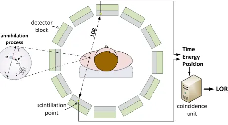
CHAPTER 1 INTRODUCTION The working principle of PET is briefly illustrated in Figure 1:. First, the tracer is injected into the subject, where the blood flow distributes it through the body according to its biochemical properties. Then, when a radioactive atom of the tracer decays, a positron is emitted from the nu-cleus and, after travelling a short distance (typically between a few tenths of a millimeter up to several millimeters [Phe06]), it combines with an electron. The process that follows is known as annihilation, in which both the positron and the electron are annihilated and a pair of 511 keV gamma photons is emitted in opposite directions (180o apart).
Figure 1: PET working principle.
The PET scanner needs to detect both emitted photons of the pair to establish the line of response (LOR) along which the annihilation took place. After millions of LORs are acquired, a tomo-graphic 3D image of the subject can finally be formed, revealing the places where annihilations occurred (i.e. where the tracer concentration was higher).
generat-1.1 POSITRON EMISSION TOMOGRAPHY
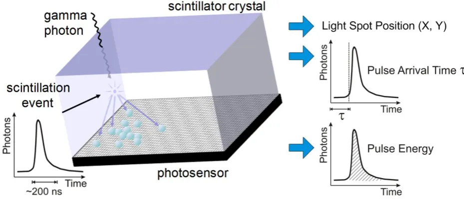
The detectors most widely used in PET scanners are scintillation detectors [Phe06], which are composed by a dense crystalline scintillator material coupled to a photodetector. The scintillator is a material that absorbs the incoming high-energy gamma photons and emits low-energy pho-tons (light) as a result. The scintillation light is emitted isotropically in a short pulse in time, typ-ically a couple hundred nanoseconds long [Phy11], as illustrated in Figure 2.
Figure 2: Scintillation light pulse hitting the photosensor and its respective outputs.
The amount of light photons that is emitted from a single 511 keV gamma absorption is typically very low, varying between 1k to 30k photons depending on the scintillator material [Phy11]. Therefore, the first requirement for PET photosensors is to possess a very high sensitivity in or-der to achieve a good signal-to-noise ratio (SNR).
Another important requirement for the photosensor concerns its timing performance. The recent development of bright and fast scintillators such as LSO, LYSO and LaBr3 has enabled the usage
of Time of Flight PET (ToF-PET), which explores the difference between the arrival times of the gamma pair to estimate the position along the line-of-response (LOR) where the annihilation took place. Therefore, to actually improve the signal-to-noise ratio (SNR) and image contrast with ToF-PET, the employed detectors must feature sub-ns timing performance [Mos07].
ma-CHAPTER 1 INTRODUCTION Finally, it is important to note that PET is usually performed alongside CT for body anatomy in-formation. A recent goal of biomedical imaging research is, however, the PET-MRI integration, as MRI, with respect to CT, offers better soft tissue differentiation and does not incur an addi-tional dose of radiation to the patient [Pic+08]. This goal brings an addiaddi-tional requirement for PET photosensors: the compatibility with the magnetic fields generated by MRI.
1.2.The proposed solution
The PET detector developed in SPADnet is scintillator-based, and thus the requirements briefly summarized in the previous section for the light sensor all apply to the solution presented in this thesis. Moreover, the scintillator material selected to form the PET detector for SPADnet was LYSO. LYSO has several advantages that make it a popular scintillator in PET applications: high stopping power (density), high light yield and fast decay time, among others [Phy11]. LYSO is also non-hygroscopic, making its manipulation during experimental measurements much easier than with its hygroscopic counterparts, such as LaBr3(Ce). On the other hand, LYSO
contains the radioactive isotope 176Lu, and thus emits background radiation which must be taken into account when designing the sensor architecture.
To best meet the requirements for a PET detector, a comprehensive modeling of the energy and timing performance of single-photon sensors for PET is initially performed. This modeling al-lows the definition of guidelines for the sensor design, aiming at the ideal parameter compromis-es. Based on the defined guidelines and requirements, a top-to-bottom architecture using CMOS technology and SPADs is proposed. The architecture incorporates in-pixel spatio-temporal com-pression of SPAD pulses for increased fill-factor, per-pixel timestamping of photons for im-proved timing resolution and top-level monitoring of the photon flux for efficient scintillation detection.
The first implementation of this architecture is done in the form of the SPADnet-I, which is a 8×16-pixel sensor fabricated in 0.13 μm 1P4M CMOS imaging technology [Bra+14]. The SPADnet-I is also able to offer a real-time output of the total detected energy that can be used for pile-up rejection and scintillator decay time estimation.
1.3 STRUCTURE OF THE THESIS
developed techniques, the complete characterization of the sensor is performed, where the best performance values obtained are an energy resolution of 10.8% and a coincidence resolution time of 288 ps.
1.3.Structure of the Thesis
Chapter 2 State of the Art
Historically, the most commonly used light sensors in PET scanners were photomultiplier tubes (PMTs) [Del+09]. A typical PMT is formed by a vacuum tube containing a photocathode, which emits an electron for each incoming photon, followed by electron multipliers, which multiply each electron up to millions of times [Phe06], and an anode, which is the collector electrode. The very high gain provided by the electron multipliers equates to a very high sensitivity, along with low noise and fast response.
However, since PMTs are composed of vacuum tubes, they are somewhat bulky and fragile. In addition, they also require power supplies of many hundred volts and are sensitive to magnetic fields – meaning their use in PET-MRI scanners is difficult. Due to these disadvantages, solid-state detectors (SSDs) have long been proposed as an alternative to PMTs [Lig+86].
SSDs are intrinsically compact and rugged, besides being insensitive to magnetic fields and usu-ally requiring lower operating voltages. One of the first SSDs to be proposed as a light sensor in PET scanners was the avalanche photodiode (APD). APDs provide reasonable timing resolution and gain, which are, however, substantially worse than in PMTs [Ber+08]. As such, research in the field of SSDs for PET has been very active in the last years, and a new type of SSD recently suggested for PET has been showing promising results: the Silicon Photomultiplier (SiPM) [Ott+04]. As this is the type of detector targeted in this thesis, a detailed discussion about its state-of-the-art is given in the next section.
2.1.Silicon Photomultipliers
CHAPTER 2 STATE OF THE ART
(a)
(b)
Figure 3: analog (a) and digital (b) SiPM architectures.
The performance of PET detectors heavily depends on the type and dimension of the scintillator crystal used in the measurements. Therefore, for an unbiased figure-of-merit (FOM) comparison between SiPM-based PET photosensors, an LYSO crystal with 3×3×5 mm³ size will be used as a standard. Focusing first on the detectors coincidence resolving time (CRT, also known as timing resolution), [Sei+12a] reports a CRT of 138 ps using Hamamatsu SiPMs, while [Yeo+12] reports 183 ps using SensL devices and [Gol+13] obtained 186 ps with FBK-SRS SiPMs. Other works have focused on energy resolution characterization, another important FOM for PET, with [Ser+13] reporting 10.2% also with FBK-SRS SiPMs, and [Szc+13] reporting 10.5% with Ha-mamatsu sensors (with a 5×5×5 mm³ crystal, however).
Other companies are also working on SiPM development, such as Excelitas Technologies [Exc14], or KETEK [Ket14]. In general, though, the performance of the various SiPM manufac-turers in PET applications is relatively similar, and the above comparison of SiPMs in similar measurement conditions is very representative of the state-of-the-art of the technology.
2.1 SILICON PHOTOMULTIPLIERS
is only able to distinguish between a photon and no photon (i.e. it is an intrinsically binary out-put), performing the A/D conversion at each individual SPAD can significantly improve the noise performance of the system. This approach has been recently pursued in [Fra+09], with the so-called “digital SiPM”, schematically shown in Figure 3(b).
The digital SiPM takes advantage of CMOS technology to perform a 1-bit A/D conversion per SPAD and to integrate an on-chip digital accumulator that produces the sensor energy output. In addition, the timing information is also generated on-chip, by a time-to-digital converter (TDC), and there are per-SPAD memories that can disable noisy devices, further improving performance and device yield. One disadvantage of the digital SiPM is that the fabrication process cannot be fully customized for optimum SPAD performance, as is the case of the dedicated analog SiPM, since the digital SiPM requires CMOS technology.
Up to now, only one group has successfully developed and characterized a digital SiPM for PET, reporting a CRT of 153 ps and an energy resolution of 10.4% [Hae+12], also with a 3x3x5 mm³ LYSO crystal. Other groups have also been pursuing the digital SiPM approach [Man+12], [Bér+12] without, however, having reported PET characterization results yet. Finally, CMOS SiPMs have also been reported for different applications, such as fluorescence lifetime imaging [Tyn+12].
CHAPTER 2 STATE OF THE ART
Table 1: comparison of the PET performance of state-of-the-art SiPMs using LYSO crystals of approximately 3×3×5 mm³.
Manufacturer Refs. Analog (A)/
Digital (D) CRT
Energy resolution
Hamamatsu [Sei+12a], [Szc+13] A 138 ps 10.5%
SensL [Yeo+12] A 183 ps -
FBK-SRS [Gol+13], [Ser+13] A 186 ps 10.2%
Chapter 3 Gamma Detection in PET Scanners
The goal of a PET photodetector is to sense the arrival of a gamma photon, and then estimate three of its features: energy, time of arrival and incident position. Given the structure of scintilla-tion detectors, these tasks are all appointed to the light sensor, which must perform them based on the light incoming from a scintillation event. In the following sections, the main issues re-garding each of these tasks will be analyzed, along with the resulting requirements for the sensor. The main goal of these analyses will be to define a set directions for the sensor architecture and design, which will then be discussed in Chapter 4.
3.1.Gamma Discrimination
As gamma photons arrive randomly in time, in a completely asynchronous fashion, it is crucial that the PET photodetector be event-driven so as to only provide data to the system when an ac-tual 511 keV scintillation occurs. This ensures that the next level of the system hierarchy (in the case of SPADnet, the module FPGA) is not overflown with data. Moreover, depending on the sensor architecture, the sensor readout operation may result in a detection dead time, which can be further detrimental to the PET system performance. To identify the best strategy for gamma discrimination, in the next paragraphs a model for the scintillation event will be defined.
The light pulse emitted from a scintillator when a gamma photon is absorbed can usually be de-scribed as the convolution of two exponential functions [Hym65]: one representing the gamma energy transfer – which translates into the pulse rise time – and another representing the crystal radiative decay – which translates into the pulse decay time. The equation for the photon flux
reaching the photosensor can then be written as in (1), where is the time of absorption
of the gamma photon, is the scintillator rise time, is the scintillator decay time and is
the total number of detected photons after a sufficiently long integration time (i.e. much larger than ).
3.1 GAMMA DISCRIMINATION
At the same time, the photodetectors are constantly subject to noise, both from the readout cir-cuits as from the photodetection devices (e.g. the SPADs) themselves. The combination of these noises can manifest itself as a signal equivalent to that of a few light photons, resulting in overall flux similar to the curve shown in Figure 4.
Figure 4: expected flux (photon and noise) at the photosensor when an event occurs at time Θ.
The first point to notice from this graph is that the gamma discrimination function may be a sim-ple threshold, as long as the scintillation flux is sufficiently stronger than the noise level. In other words, the first requirement of the sensor is that its signal-to-noise ratio must be high enough so that the random variations in the noise level do not generate false positive events.
However, intrinsic to the discrimination concept described above is that the sensor must be able to detect the flux of incoming photons. This is a not obvious feature in typical image sensors (e.g. standard CMOS image sensors [ElG+05] or SPAD pulse counters [Sto+09a], [Pan+11]), which are integrating sensors, that is, they contain an analog integrator or digital counter at their output. These sensors would have an output with the form of Figure 5 (i.e. the integral of Figure 4). As the arrival time occurs randomly in time, one does not know when to “start counting” (or, more precisely, when to reset) so that a threshold can be efficiently compared.
Finally, depending on the crystal size and in the optical coupling between sensor and crystal, the scintillation photons will be spread in a relatively large area in the sensor. Therefore, the discrim-ination of a gamma event requires a sensor with (1), a high SNR, (2), photon flux monitoring, and (3), that this monitoring occurs on a relatively large area.
flu
x
time
avg noise level
CHAPTER 3 GAMMA DETECTION IN PET SCANNERS
Figure 5: expected counting output based on the flux of Figure 4, for a gamma event arriving at two different
times, Θ1 and Θ2.
3.2.Energy Estimation
Although identifying the gamma energy may not seem crucial to PET systems, since all gamma rays emitted from the annihilation process have 511 keV, gamma rays can also interact with mat-ter through Compton scatmat-tering, which results in the gamma photon losing part of its energy and changing its travel direction. This means that there are a few possible scenarios for scintillation events at a PET detector:
(a) an unscattered gamma photon is fully absorbed by the scintillator through the photoelec-tric effect;
(b) a previously scattered (e.g. at the body) gamma is absorbed by the scintillator;
(c) a gamma photon goes through Compton scattering in the scintillator, and then escapes it;
(d) a gamma photon goes through Compton scattering in the scintillator and then is fully absorbed by it.
As should be expected, events of type (a) are the ideal ones, enabling the maximum SNR and a correct reconstruction of the LOR. Type (b) events must absolutely be discarded, since they changed direction along their path to the scintillator and would provide an incorrect LOR. Type (c) events could be used to reconstruct an LOR, even if their SNR would be lower due to the smaller deposited energy. However, there is no way to distinguish (c) events from (b) ones, and thus (c) events must also be discarded. Finally, for (d)-type events, the correct LOR could be
re-tot
al c
oun
ts
time
0 0 0
3.2 ENERGY ESTIMATION
constructed if the position of the first deposition site could individualized. Given the speed of light of the gamma photons, though, current state-of-the-art sensors do not feature the required timing resolution for this.
The physics behind the Compton scattering process that occurs in scintillators results in scattered events of up to 340 keV [Wer+04]. Additionally, when using a scintillator with intrinsic radioac-tivity, the scintillator-emitted gamma photons will also generate events that need to be discarded. In the case of LYSO, its intrinsic radiation will emit photons with 88, 202 or 307 keV [Pre08]. Therefore, in PET systems, low-energy events must be distinguished from unscattered, 511 keV gamma absorptions and then discarded. It should be noted that (d)-type events actually cannot be distinguished through their energy, as the full 511 keV were deposited in the scintillator. There-fore, the scintillation position information, which will show two separate deposition sites, must be used to discard these events.
A typical energy spectrum obtained in a PET system is shown in Figure 6 [Med10]. As can be observed in the graph, both the scattered range upper-limit of 340 keV as well as the 511 keV peak are not very sharp, and are actually merged. To describe this energy estimation uncertainty, the energy resolution figure-of-merit (FOM) is typically used, which is obtained by dividing the full-width-at-half-maximum (FWHM) of the 511keV peak of the energy spectrum by the peak value itself. As such, the smaller is the detector energy resolution, the better is its energy estima-tion.
Figure 6: Typical energy spectrum obtained in a PET scanner, with an energy resolution of about 20%.
FWHM
CHAPTER 3 GAMMA DETECTION IN PET SCANNERS The energy estimation uncertainty in a PET detector is the result of the many stochastic process-es prprocess-esent between the emission of light photons by the scintillator and their detection by the photosensor. Moreover, as shown by the merging of the peaks in the spectrum above, this uncer-tainty leads to a non-optimal filtering of low-energy events, possibly leading to a deterioration of the final PET image quality. Therefore, an investigation of these processes is merited, and will be performed next. To simplify this discussion, the photosensor will be assumed fully digital, i.e. it will be considered a digital counter with negligible readout electronic noise.
In a PET detector, the energy estimation comes from integrating the incoming flux shown in Figure 4. Therefore, two main processes will contribute to the final estimation: the photon flux itself and the photodetector noise. Given the digital counter assumption, the main source of un-certainty in both these process will be shot noise, which follows a Poisson distribution. Moreo-ver, the scintillator itself is also a source of uncertainty due to the intrinsic variation in the num-ber of emitted low-energy photons for the same absorbed gamma energy.
As these three processes are independent and uncorrelated, their variances can be summed to ob-tain the total energy variance. From this, and since in a Poisson distribution the variance is equal to the mean, the energy resolution of a detector can be written as in (2).
[(
√
) ] (2)
3.2 ENERGY ESTIMATION
Equation (2) can be used to estimate the achievable energy resolution using and as input parameters. This is shown in the contour plot in Figure 7, where the scintillator was con-sidered LYSO, with an intrinsic energy resolution of 8% [Nas+07].
Figure 7: Contour plot of the expected energy resolution versus the number of photon and noise counts.
The graph shows that up to about 10 noise counts per event, the energy resolution is not affected by photodetector noise. From this point onwards, the resolution starts worsening relatively fast with the noise counts in log scale, in accordance with the square root relation of equation (2). On the other hand, with respect to photon counts, the energy resolution changes very slowly for high photon counts, and then worsens somewhat exponentially as photon counts go down in linear scale (this is shown by the constant resolution black lines getting closer to each other).
These considerations make it clear that the intrinsic scintillator resolution is by far the most lim-iting factor for the detector energy resolution, at least when considering state-of-the-art SiPMs such as the ones referenced in Chapter 2. Nonetheless, to achieve an energy resolution at least as good as the state-of-the-art (i.e. slightly above 10%), the digital counter sensor must detect around 1500 photons with not much more than 100 noise-generated counts.
noise counts
p
h
o
to
n
co
u
n
ts
energy resolution [%]
10-1 100 101 102 103
100 400 700 1000 1300 1600 1900
10 15 20 25
Enres = 12
Enres = 13
Enres = 11
Enres = 10
CHAPTER 3 GAMMA DETECTION IN PET SCANNERS
3.3.Time of Arrival Estimation
Obtaining the time of arrival (ToA) of a gamma photon is crucial to the workflow of a PET scanner, since the coincidence unit of the system uses this information to match two detected gammas in opposite detectors of the ring, as explained in Chapter 1. Similarly to the energy reso-lution, the timing resolution of a detector indicates the uncertainty with which the time of arrival information is estimated. Therefore, the better is the timing resolution of the system, the smaller can the coincidence window be made, thus reducing the amount of false coincidences and im-proving the image quality of the system.
From the perspective of the coincidence window alone, i.e. with standard PET scanners, even a relatively low resolution of a few nanoseconds can provide a reasonably good imagine quality [Lew08]. However, in ToF-PET the detector timing resolution has a much greater importance, as the time difference between the pair of detected gammas is used to estimate the position of the annihilation process along the LOR. This way, the detector timing resolution directly impacts the final image quality.
For an effective ToF-PET detector, the timing resolution must be at most a few hundred picosec-onds [Mos07], since, for instance, a resolution of 500 ps results in an uncertainty (FWHM) of about 7.5 cm, which is still an order of magnitude higher than the resolution achieved by PET systems through the processing of several LORs [Spa+10]. Therefore, in recent years there has been a strong research push towards improving timing resolution in PET scanners.
Before modeling the ToA estimation, an important distinction must be made between the system (or coincidence) timing resolution and the single detector resolution. The final desired figure, i.e. the time difference between the pair of detected gammas, is obtained from the subtraction of the ToA estimations of the two gammas in coincidence. As such, the system timing resolution – also known as the coincidence resolving time, the CRT – is composed by a linear combination of two stochastic processes. As the two ToA estimations are completely independent, assuming also that the two opposite detectors are identical, the CRT can be written as in (3).
3.3 TIME OF ARRIVAL ESTIMATION
This again assumes that the underlying distribution is Gaussian, and thus the 2.35 factor is used to convert the standard deviations and into the FWHM, which describes the CRT. It should be noted that this conversion is not usually necessary during characterization or in simu-lations, as the actual CRT distribution can be obtained and the FWHM taken directly. Nonethe-less, as will be shown later, this distribution is anyway typically very well fitted by a Gaussian. Given the above considerations, in the next subsections the single detector timing resolution, de-scribed by , will be modelled and analyzed, so as to identify the best compromises in the de-tector design. This modelling will focus on three processes: the emission of photons by the scin-tillator, the detection of the photons by the sensor and the sensor temporal noise, which may generate noise timestamps that are indistinguishable from photons ones.
3.3.1Timestamp Model
The first and most important process that affects the timing resolution in PET detectors is the emission of photons by the scintillator. This process was already described in terms of the flux that reaches the sensor, in section 3.1. To model the uncertainty in the timing estimation, equa-tion (1) can be rewritten as the probability density funcequa-tion (PDF) of the emission of each photon
| , with each emission being independent and identically distributed (i.i.d.) [Fis+10].
|
(4)
The corresponding cumulative distribution function (CDF) can be written as:
| ∫ ̂| ̂
(5)
CHAPTER 3 GAMMA DETECTION IN PET SCANNERS ing, different processes will occur at the sensor (e.g. SPAD avalanche, signal transmission, TDC triggering) that will contribute to jitter in the final timestamp. As these processes are generally random and independent, for the proposed model they will be approximated by a single Gaussian distribution , with mean and standard deviation , as written in equation (6) [Sei+12a]. Considering that the photon is absorbed at , to maintain causality, it is assumed that (so that ).
√
( )
(6)
Since the photon timestamp is the sum of the photon emission with the detector jitter, the result-ing distribution is given by the convolution of the two underlyresult-ing distributions. Therefore, the
PDF | and CDF | of the photon timestamp can be written as shown below, with
the full mathematical development of these equations provided in Appendix A.
| ∫ |
(7)
| ∫ |
(8)
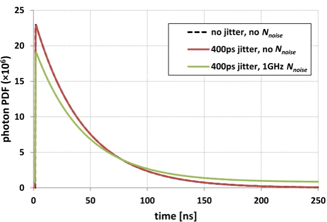
The effect of the detector jitter in the photon timestamp PDF is graphically shown in Figure 8. In this figure, the PDF is plotted for three cases: no jitter, a jitter of 200 ps FWHM and a jitter of 400 ps FWHM. As can be observed, the overall shape of the PDF hardly changes, however the rising time is made progressively slower. As will be shown in the analysis section below (3.3.3), this causes a significant worsening of the system CRT.
3.3 TIME OF ARRIVAL ESTIMATION
Figure 8: Comparison of the photon timestamp PDF with and without detector jitter.
This temporal noise manifests itself uniformly over time, and thus is described by the uniform distribution. However, for the PDF of the uniform distribution to have a non-zero value, it should be limited to a finite time interval. As such, for the proposed model, noise-generated timestamps will be assumed to occur only during a finite integration time , that starts together with the
scintillation and finishes after effectively all photons have been detected (i.e. ). This implies that, for the actual ToA estimation procedure, it is possible to remove any noise timestamp that occurred before the scintillation itself, while the ones generated during the scintil-lation event will be undistinguishable from photons. As will be shown later in the experimental results chapter, this is not an unrealistic hypothesis. The resulting noise PDF equation is shown in (9).
| {
(9)
CHAPTER 3 GAMMA DETECTION IN PET SCANNERS
∑
(10)
Given that the proposed model defines a fixed integration time for the noise distribution, the weights can simply be taken as the ratio between the number of photon and noise counts [Man+13]. Moreover, for simplification reasons, the mixed distributions are considered to be
| and | directly, meaning that the noise timestamps are not convolved with the
system jitter. This should not affect the final result, as the noise timestamps are already com-pletely random in time, and additionally, it will allow for an interesting simplification of the final PDF equation. The photon plus noise timestamp distribution can then be written as:
|
|
|
(11)
It is interesting to note that, since is simply the integral of the noise flux during the de-fined integration time, a noise occurrence rate can be defined so that . Since | ⁄ during the integration time, equation 10 can be rewritten, for this same interval, as:
|
( | )
(12)
3.3 TIME OF ARRIVAL ESTIMATION
Figure 9: Comparison of the photon timestamp PDF with and without detector jitter and with and without
temporal noise.
3.3.2Methods for Timing Resolution Assessment
The model described in the previous subsection only provides a distribution for the timestamps that will be obtained by the system. Therefore, a method it is still required to assess how this dis-tribution actually translates into the system timing resolution. Two different methods will be considered depending on how the detector estimates the gamma ToA. In the first scenario, the detector uses only a single timestamp for estimation, while in the second all timestamps can be obtained and then combined to provide an improved gamma ToA estimation.
Even if the second scenario may seem the best, in real systems, providing all timestamps can heavily degrade other system parameters, such as the photon detection efficiency (PDE) due to degraded fill-factor (FF). As this compromise completely depends on the actual implementation of the photosensor, it is out of the scope of this chapter and will be left for later discussion. The goal of this subsection is to provide the methods for assessing the timing resolution with respect to the various parameters present in the model described above, such as the jitter standard devia-tion and the noise occurrence rate, and not to compare the merits and disadvantages of different ToA estimation techniques.
Starting with the scenario of single-timestamp estimation, the theory of order statistics [Arn+92] can provide the tools to quantify the uncertainty that each ordered timestamp will exhibit.
Con-0 5 10 15 20 25
0 50 100 150 200 250
pho
ton
PDF (
×10
6)
time [ns]
no jitter, no
400ps jitter, no
400ps jitter, 1GHz Nnoise
Nnoise
CHAPTER 3 GAMMA DETECTION IN PET SCANNERS PDF of the i-th order timestamp is given by equation (13), where and are the PDF and the CDF of the unordered timestamps.
|
{ } { } (13)
Considering a system where a single timestamp is used as the gamma ToA, but where this timestamp can be selected to be a specific order of the incoming flux of timestamps, the variance of the distribution in (13) can be used as an estimate of the detector timing resolution [Fis+10]. For a detector that can timestamp all its detected photons, the Cramér–Rao bound (CRB) can ex-press the lower limit on the variance of an unbiased estimator of the gamma ToA [DeG86]. In other words, given an unbiased estimator for the gamma ToA that combines all detected timestamps, its variance will be equal to or higher than the CRB. The CRB is defined as in equa-tion (14), where ̂ is the unbiased estimator of , and is the Fisher information regarding
of all timestamps.
̂
(14)
The Fisher information of all timestamps, in turn, is defined as in equation (15) [Sei+12b].
∫ [
| ] |
(15)
3.3 TIME OF ARRIVAL ESTIMATION
3.3.3Analysis
Using the model and methods described in the previous subsections, it is now possible to inves-tigate how the detector parameters will influence its timing resolution. Namely, the number of detected photons, the detector noise rate and the detector jitter will be analyzed with regards to their impact in the resolution. For all analyses, a LYSO scintillator will be assumed, featuring a rise time ( ) of 90 ps and a decay time ( ) of 43 ns [Sei+12b]. In addition, all resolution values will be reported in terms of CRT assuming two identical detectors so as to allow for easier com-parison with experimental results both from this thesis as from the literature.
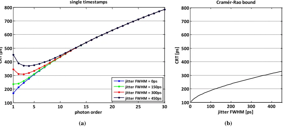
To first analyze the photodetector PDE (i.e. the number of detected photons ) isolated from other parameters, the scintillation emission distribution | described in (4) can be applied to the order statistics and CRB methods. In Figure 10, the FWHM of the first 30 orders along with the CRB translated to the FWHM assuming a Gaussian distribution is plotted for a total number of detected photons of 1000.
Figure 10: CRT considering only the photon emission process with 1000 total detected photons.
It can be observed that the first ordered statistic features the best single timestamp resolution, a behavior that can be shown to occur for any value of . Moreover, the first photon resolution is about 67% higher than the CRB, a behaviour which, however, changes depending of Nph. Thus, in Figure 11, the resolutions obtained with the CRB and with the first photon are plotted versus a varying number of total detected photons. In this graph, the first photon can be from up
1 5 10 15 20 25 30
100 200 300 400 500 600 700 800
photon order
C
R
T
[p
s]
CHAPTER 3 GAMMA DETECTION IN PET SCANNERS worse at the maximum plotted number of total photons ( ). In any case, both curves present a plateauing effect towards high photon counts, indicating that gains in detector PDE af-ter a certain point have diminishing returns.
Figure 11: CRT with the first photon and the CRB considering only the photon emission process with a
varying number of total detected photons.
Next, the photon with jitter distribution, | , can be used to analyze the impact of the sys-tem jitter in the ideal detector CRT discussed above. Similarly to what was done in Figure 10, the graph below plots the single timestamps CRT versus photon order, as well as the CRB, with 1000 detected photons, but now for different jitter values.
(a) (b)
Figure 12: CRT of the single timestamps (a) and of the CRB (b) considering the photon emission and the
0 500 1000 1500 2000
0 100 200 300 400 500 600 700 800
number of detected photons (Nph)
C R T [p s] first photon Cramér-Rao Bound
1 5 10 15 20 25 30
100 200 300 400 500 600 700 800 photon order C R T [p s] single timestamps
jitter FWHM = 0ps jitter FWHM = 150ps jitter FWHM = 300ps jitter FWHM = 450ps
0 100 200 300 400
100 200 300 400 500 600 700 800
jitter FWHM [ps]
CR
T
[p
s]
3.3 TIME OF ARRIVAL ESTIMATION
With respect to the single timestamps, the addition of jitter into the model results in not only the worsening of the best CRT, but also that the first photon is no longer the best, with the best order increasing as the jitter increases. Interestingly, though, the jitter only affects the CRT of the ini-tial timestamps, with the resolutions from the 10th order and above being approximately equal. Regarding the CRB, the resolution worsens less than linearly with jitter, but still, a jitter of around 400 ps FWHM can worsen the CRB resolution more than three times.
To obtain a complete picture of the CRT versus both the detector jitter and PDE, Figure 13 shows a contour plot of the single timestamp CRT versus these two parameters. To improve vis-ualization, only the CRT of the best order is used, and thus, for reference, Figure 14 shows the order of the best timestamp CRT used in each data point.
As can be observed, the weight of the detector jitter in the CRT increases rapidly as the number of detected photons increase: for very low , the CRT is almost constant with respect to jitter, while at high photon levels the CRT quickly degrades with jitter values as low as 50 ps. Moreo-ver, the trend shown with the photon-emission-only model in Figure 11 is also clear in Figure 13, where, for a constant jitter value, the CRT worsens approximately exponentially when de-creases. To complete the analysis of the detector PDE versus jitter, Figure 15 plots the same con-tour plot as in Figure 13, but now using the CRT obtained through the CRB method.
Figure 13: CRT of the best single timestamp considering the photon emission and the system jitter versus the number of detected photons (Nph)
d e te ct o r ji tt e r (F W HM ) [p s]
best single photon CRT [ps]
500 1000 1500 2000 2500
50 100 150 200 250 300 350 400 450 500 550 600 200 300 400 500 600 700 800 900 1000
CRT = 150 ps CRT = 2
00 ps
CRT = 250 p
s CRT
CHAPTER 3 GAMMA DETECTION IN PET SCANNERS
Figure 14: order of the timestamp used in Figure 13.
The CRB behavior differs from the best single photon one in two significant ways: first, as ex-pected, a given CRT value can be obtained with a lower PDE or higher jitter, when compared to Figure 13. Secondly, for low values of jitter, the trend changes completely, with the CRB CRT continuously improving down to zero jitter. Of most importance, though, is that both analysis methods clearly show that, to obtain a CRT comparable with the state-of-the-art, not only is a reasonable PDE required – providing around 1500 detected photons – but also a low detector jit-ter, near or below 100 ps FWHM, should be targeted.
Finally, to analyze the effect of the temporal noise rate, , in the timing resolution, the dis-tribution model | is used. Due to the way that the noise uniform distribution was de-fined in this model, with a fixed starting point, the ordered timestamp method cannot be used to estimate the CRT, as the timestamp distributions will be strongly biased towards this starting point. The CRB method, on the other hand, evaluates the overall uncertainty that having noise during a scintillation event would add to an unbiased estimator, and thus does not depend on the noise starting point. As such, in Figure 16 the CRB CRT is plotted versus for 1000 detect-ed photons and different values of the detector jitter.
number of detected photons (Nph)
d e te ct o r ji tt e r (F W HM ) [p s]
order of the single photon with best CRT
500 1000 1500 2000 2500
3.3 TIME OF ARRIVAL ESTIMATION
Figure 15: CRT of the Cramér-Rao bound considering the photon emission and the system jitter versus the
number of detected photons and the jitter FWHM.
Figure 16: CRT of the Cramér-Rao bound considering the complete model (photon emission, jitter and noise)
with 1000 total detected photons and different values of jitter.
The curve clearly shows that up to a noise rate of about 100 MHz, the temporal noise has little effect on the CRT. However, from this point onwards, the relationship is close to an exponential. This trend is repeated for all jitter values, with each curve differing only by its starting level.
number of detected photons (Nph)
d e te ct o r ji tt e r (F W HM ) [p s]
Cramér-Rao bound CRT [ps]
500 1000 1500 2000 2500
50 100 150 200 250 300 350 400 450 500 550 600 100 200 300 400 500 600 700 800 900 1000
CRT = 1 50 ps
CRT = 200 p
s
CRT
= 25
0 ps
CRT = 30
0 ps
CRT = 100 ps
101 102 103 104 105 106 107 108 109 1010
100 200 300 400 500 600
noise rate [Hz]
C
R
T
[p
s]
CHAPTER 3 GAMMA DETECTION IN PET SCANNERS Therefore, the next and final analysis plots the contour plot of the CRT versus the number of de-tected photons and the noise rate, with a fixed jitter FWHM value of 150 ps.
Figure 17: CRT of the Cramér-Rao bound considering the complete model (photon emission, jitter and noise)
versus the number of detected photons and the noise rate, with a fixed jitter FWHM of 150 ps.
Figure 17 confirms the previously observed trend that the noise only starts affecting the CRT af-ter around 100 MHz for any number of detected photons, although, for high photon counts, this trend is much less steep. It is also interesting to compare the above plot with the equivalent one for the energy resolution in Figure 7. Both are relatively similar, taking into account that, with a typical integration time of 150 ns, the top of the x-scale for the energy resolution, 1000 counts, equals a 7 GHz rate in the CRT x-scale. However, at high noise levels, the noise contribution to the CRT increases much more rapidly than to the energy resolution.
3.4.Position Estimation
The final piece of information that the photosensor needs to provide about the scintillation is the position. In a typical PET detector ring, as the one shown in Figure 1, each detector block can be as large as 25 cm on each side [Wer+04]. Therefore, knowing the scintillation X and Y position – i.e. the position with respect to the sensor plane – is essential to correctly build the LOR. The
noise rate [Hz]
n u m b e r o f d e te ct e d p h o to n s (N p h )
Cramér-Rao bound CRT [ps]
101 102 103 104 105 106 107 108 109 1010 100 500 1000 1500 2000 2500 200 300 400 500 600 700 800 900 1000
CRT = 100 ps
CRT = 150 ps
CRT = 200 ps
3.4 POSITION ESTIMATION
precision of the LOR will be mainly given by the detector spatial resolution, which is then one of the key parameters determining the scanner final image quality. However, there are two physical limitations in the LOR reconstruction that need to be addressed first: positron range and gamma emission non-colinearity.
Positron range accounts for the small distance that a positron travels between its emission and is annihilation. As the gamma pair is emitted from the annihilation site, the LOR is actually indicat-ing this position as opposed to the positron decay one. Even though the positron undergoes mul-tiple direction changes until it is annihilated, the positron range is defined as the Euclidean dis-tance between the decay and the annihilation sites, as the error in the LOR reconstruction is a function of this distance. Moreover, as it is a stochastic process, the value usually quoted as posi-tron range is the FWHM of its distribution [Phe06]. Finally, the posiposi-tron range depends on the radionuclide used, and the spatial resolution loss that it causes in the final PET image is usually between a few tenths of a millimeter up to several millimeters [Phe06].
The non-colinearity, on the other hand, accounts for the fact that the pair of gamma photons will not be emitted at exactly 180o, and will, in fact, be emitted with a distribution of angles with a mean of 180o and a FWHM of 0.5o [Phe06]. Since the LOR reconstruction assumes perfectly op-posite gammas, this effect will also produce an intrinsic spatial resolution error. This error de-pends on the diameter of the PET ring, and can be approximated as [Phe06]. Thus, for clinical PET systems with diameters in the order of 90 cm, the error becomes close to 2 mm, while for pre-clinical PET, with diameters closer to 20 cm, it is smaller than 0.5 mm.
In light of these effects, it is clear that the goal for the detector spatial resolution is considerably loosened depending on the PET application. Nonetheless, the factors influencing the detector spatial resolution will be discussed below, assuming a pre-clinical PET system, which presents a smaller intrinsic spatial error.
CHAPTER 3 GAMMA DETECTION IN PET SCANNERS However, the spatial resolution of scintillation detectors depends even more strongly on the crys-tal geometry, which can generally be categorized into two main groups: needle or continuous crystals. In the needles configuration, an array of small crystals (typically around 1 × 1 mm² in pre-clinical applications [Wer+04]) is tightly packed together and placed above the photodetec-tor, with each needle surrounded with reflective material so there is no light sharing between needles. In the continuous configuration, a large, continuous crystal is coupled to the photodetec-tor to form the detecphotodetec-tor block. In both cases, a light guide layer is usually inserted between the crystal and the photodetector with the aim of decreasing the photon density on the sensor surface [Lew08].
Due to the reflective coating in typical needle configurations, any X and Y intra-needle position information is lost. As such, the spatial resolution of a needle-based PET detector is a direct function of the size of the individual crystals. Additionally, the addition of a light guide results in the light from a single crystal spreading over an area much larger than the crystal itself. There-fore, the sensor pixels can be made quite large (e.g. 3.4 mm pixel pitch with 0.8 × 0.8 mm2 crys-tals in a detector prototype [Son+10] or 3 mm pixel pitch with 1.1 × 1.1 mm2 crystals in a com-mercial scanner [Nag+13]), while still providing enough information to correctly distinguish scintillations from different crystals. Alternatively, one-to-one coupling between crystal and pix-el can be used, in which case the pixpix-el pitch will match the crystal pitch [Lev+07].
On the other hand, the spatial resolution in continuous crystal configurations heavily depends on the photosensor ability to recognize the light spatial distribution on its surface. Therefore, for continuous crystal detectors, the pixel size is a much more critical parameter. Still, recent devel-opments have demonstrated continuous crystal PET detectors with a spatial resolution of 0.9 mm with pixel pitch of 1.5 mm [Llo+10], or a resolution of 1.6 mm with a pixel pitch of 3.3 mm [Sch+09]. Therefore, also in the continuous crystal case, a pixel pitch in the order of one to few millimeters is sufficient for the application.
3.5 OTHER FEATURES
Many different methods have been conceived along the years to obtain the DOI in PET scanners. For instance, two different scintillators can be placed on top of each other, and their different de-cay times used to identify in which layer the scintillation occurred, in what are usually called phoswich detectors [Sao+99], [Jun+07]. Alternatively, two crystal arrays of the same type can be arranged on top of each other with a small offset, and thus the DOI can be obtained from the X and Y position [Liu+01]. Another approach is to place photosensors in more than one crystal sur-face, in so called double-sided readout detectors, and use the photon ratio between the sensors to estimate the DOI [Del+10].
Finally, in continuous crystal configurations, the light spatial distribution depends on the DOI, and thus can be used to estimate it, with no changes in the actual detector construction [Lin+08], [Ler+05]. Nevertheless, in all these DOI-capable examples, the sensor pixel pitch was in the same range as the ones previously described in this section, indicating that DOI capability does not incur a stricter requirement for the pixel pitch.