Efficient High Level Methodology for Design, Simulation and Hardware
Implementation of Min-Sum LDPC Decoders
Abdessalam Ait Madi1, Ali Ahaitouf1, Anas Mansouri2 1 Sidi Mohammed Ben Abdellah University
Faculty of Sciences and Technology
Signals Systems and Components Laboratory B.P, 2202, Fez, V.N 30000 Morocco
2 National School of Applied Sciences of Fez
Signals Systems and Components Laboratory Fez, Morocco
{aitmadi_abdessalam, ali_ahitouf, anas_mansouri}@yahoo.fr
ABSTRACT: In this paper we propose a hardware implementation of a regular (3,6) LDPC decoder. Two processing units corresponding respectively to the variable and Check Node are designed in order to be used in Low Density Parity Check (LDPC) decoding by the Min-Sum Algorithm (MSA). These Units are fully parallel and flexible to be used for different block length when a regular (3, 6) LDPC codes are required. The two proposed units have been first designed and implemented in software by using the high level methodology Simulink tool following a modular design approach. In a second step, these blocks were wired in order to construct a decoder block for the LDPC code (10,5). These units are also described and simulated using Very High Speed integrated circuits Hardware Description Language (VHDL). These three kinds of imple-mentations show that the proposed high level approach is efficient for testing and validating digital circuits before being implemented on desired Field Programmable Gate Array (FPGA) device.
Keywords: MSA, LDPC, VHDL, Hardware, Implementation, FPGA Received: 22 June 2012, Revised 2 August 2012, Accepted 14 August 2012
© 2012 DLINE. All rights reserved
1. Introduction
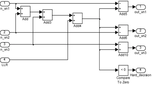
Figure 1. VNPU block diagram considering parallel configuration: update of the message sent from the VN “n” to the CN “m”
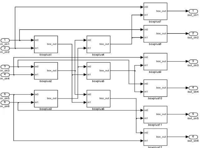
Figure 2. Boxplus diagram considering parallel configuration
Figure 3. VNPU design ms_vnp36_top in the Simulink tool for dv= 3 considering parallel configuration
combinational logic only, were introduced in order to avoid the unavoidable quantization impacts and delays. For example the MSA algorithm [5, 6] reduces greatly the hardware implementation and computation complexity, but this advantage is adversely affected by no negligible performance degradation due to the overestimation in the outgoing message from the check to variable node. Despite this drawback the MSA remains the main approximated version that consumes less area and simplifies greatly the computation complexity.
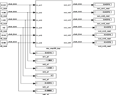
Figure 4. CNPU design ms_cnp36_top in the Simulink tool for = 6 dc considering parallel configuration
a Simulink tool for co-simulation [7] by using Electronic Design Automation (EDA) Simulator Link for direct hardware design verification. The Matlab script is used to call and connect the integrated blocks and sends stimuli to running designs to be validated and tested. As response, the designs outputs are sent back to the Matlab script. The most advantage of the co-simulation is the real system testing, therefore suppressing all possible misinterpretations present in a pure simulator. In other cases, co-simulation may be the only way to simulate a complex design in a reasonable amount of time.
For the following, in section II the processing units VNPU and CNPU for LDPC decoder are developed. The section III describes the details for the VNPU and the CNPU as well as the entire decoder designing in Simulink tool while the implementation in VHDL codes of its processing units is developed in section IV. Finally, the simulation results are shown in the section V and section VI concludes the paper.
2. Processing Units for LDPC Decoder
Iterative decoder can be constructed by considering each variable node (VN) and check node (CN) of the tanner graph [8] as processing units, and a connection between them as a bidirectional communication channels through which the processed information is sent. Since, the decoder works on the soft information, the sent messages between nodes are real values. In order to represent these values in fixed-point two’s complement representation for reduced hardware implementation, we need to quantize them authorizing, however, some performance loss as a result of the quantization.
2.1 VN Processing unit: VNPU
The architecture of the VNPU is the same as the other LDPC decoder designs [9]. In fact, the parallel design can be developed with only combinatorial logic; however, the maximum frequency will be reduced.
The dv(degree of VN) successive Lmmessages coming from the CNPU are added together with the messages Lccoming from the channel in order to calculate the variable node output value Z . The most significant bit (MSB) of Z is the sign bit which is used for hard decision to estimate the nthbit in the received word from the channel, one for the negative value and zero for the positive value. To update each output Z
nin each iteration, the corresponding message value Lmsent from the CN “m” to the VN “n” should be subtracted from Z (see figure 1). This type of implementation requires an adder Σ capable of adding dv + 1 inputs of
the length of binary fixed-point number. This means that a high number of gates is required to implement just a single processing unit, but has the great advantage of a minimum delay system high throughput.
2.2 CN Processing unit: CNPU
Figure 6. VNPU functional validation in Simulink tool
number. To implement the managed CNPU mathematical equation in hardware we separate the operationinto sign and magnitude calculations of the two incoming messages according to the following equation.
Figure 2 represents a simplified boxplus unit shown in [8] for two inputs a and b in which the overall sign Final_sign is performed by using a logical two input, sign(a)and sign(b), XOR operator. The Final_sign signal is set to zero for the positive sign and to one elsewhere. By using a mux block, the output min or – min of the comparator will be driven to the signal out taking into account the sign of the Final_sign signal value.
out = sign (a) . sign (b) . min ( | a |, | b |)
Figure 8. VNPU functional validation in ModelSim tool
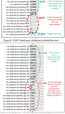
Figure 9. CNPU functional validation in ModelSim tool
To construct a modular CNPU, the boxplus unit will be instantiated in parallel manner to carry out the dc(degree of CN) messages
number of gates required increases when compared to serial or semi parallel configuration. In spite of this disadvantage, parallel configurations are still used for high throughput applications.
3. Implementation of the VNPU and the CNPU Designs in Simulink tool
3.1 VN Processing unit: VNPU
The VNPU ms_vnp36_top shown in figure 3 has been designed in Simulink using basic adder block from the Simulink library. The variable node has fourth inputs the first three in_vn1, in_vn2and in_vn3are coming from various check nodes to which
Figure 11. CNPU functional validation in HDL co-simulation using Simulink tool and ModelSim
they are connected and the fourth one is the LLR message coming from the channel communication system. The VNPU unit passes the outputs out_vn1, out_vn2and out_vn3to the check nodes and then the hard decision to estimate the nthbit in the received word is making by observing the MSB of the Z value.
To emulate quasi similar hardware functionality the blocks set used in this design works in fixed-point two’s complement format with a fixed word length set to 8 bits, the MSB bit corresponding to the sign, the next two MSBs bits represent the integer part and the five remain bits represent the fractional part. Thus, all the data will be delimited in the [minimum, maximum] interval in the 8 bit fixed-point two’s complement format. Consequently, if a value computed by the block is outside this interval, it will be immediately replaced by the maximum (respectively minimum) value achievable in the used representation, depending on the sign bit.
3.2 CN Processing unit: CNPU
The Simulink design in figure 4 represents the CNPU ms_cnp36_top. It uses various basic blocks from the Simulink library (absolute, min, xor, switch…). The block have six outputs, a positive value |out_cni| (i=1 to 6) is the minimum of the fifth value |in_cnj| ( j=1 to 6 and j # i), as example |out_cn1| isthe minimum of the set (|in_cn2|, |in_cn3|, |in_cn4|, |in_cn5|, |in_cn6|). The product
Π
sign (in_cnj), performed by the set of the XOR logic operators, represents the sign of out_cn1. All the blocks used in this design works also in 8 bits fixedpoint two’s complement representation, in the same way as the VNPU design.The functionality of these designs can be verified using Simulink tool. Once the two Simulink designs VNPU and CNPU are verified and tested, we used the Matlab script to connect them in order to construct the LDPC decoder.
3.3 Decoding Processing unit
Figure 5 shows the implementation of the decoder for the LDPC code (10,5) in parallel manner. We thus need to instantiate ten VNPUs and five CNPUs. These units will be, thereafter, wired in order to copy exactly the Tanner graph representation [9]. The messages are exchanged via wires between these two connected units. In this case, the Matlab script application is used to encode the information and create the L
cmessages coming from the simulated communication channel. These messages are the stimuli for the LDPC decoder designed in the Simulink tool. The designed decoder iterates in the Simulink tool until finding a
Figure 13. BER obtained for LDPC decoder from Matlab, Simulink,ModelSim and Simulink co-simulation
valid code word or reachingthe maximum iteration. The loop between the outputs and theinputs of the two units, used in the decoder, is allowed by using the blocks M1 to M30 which defines a memory region, for use by the Data Store Read and Data Store Write blocks used to write and read thirty Lmmessages coming from each six outputs of each CNPU unit. A strict of control of the order of execution of the data reads and writes is required. That is if a data store’s read occurs before its write, latency is introduced into the algorithm: the read obtains the value that was computed and stored in the previous time step, rather than the value computed and stored in the current time step. Such latency may causes the system destabilization and avoid correct operating. For example, an error may occur during simulation when the data store is read before being updated by the Data Store Write. As a guard against these errors we introduce a set of delay unit associated with the Data Store Read.
Each input Zn of the VNPU unit receives one Lmmessage read from the Data Store Read associated to the CNPU unit to which it is connected. Note that the VNPU inputs and outputs are respectively denoted Li(i =1 to 3) and i Z (i =1 to 6) , when the CNPU inputs and outputs are denoted Zi(i =1 to 6) and Li(i =1 to 6).
4. Implementation of the VNPU and the CNPU Designs Using VHDL Codes
The work consists of transforming the two developed designs into computerized representation by using the Very High speed Hardware Description languages (VHDL). The blocks used in these designs are described and tested individually following a modular approach. After checking the eventual errors and warnings in each module, all the elements were wired to produce the required top designs. The VNPU top design ms_vnp36_top includes six adders, three unary minus operator and one comparator to zero which is used to make the hard decision. The CNPU ms_cnp36_top include twelve instantiated boxplus unit connected by internal signals. Each boxplus is implemented according to the figure 2. All theblocks used in this designs works in 8 bits fixed-point two’s complement representation.
5. Results and Discussions
5.1 Validation of the Simulink design
The Simulink environment is used in this design approach. On figure 6, the test vector (0.5,-1, 1,-1) is applied to the VNPU unit designed in the Simulink tool, the outputs are (-1, 0.5, 1.5, 1). From this result, one can see that the estimated bit value is one. We can also see the equivalent in 8 bits fixed-point of the inputs in (in1_sf, in2_sf, in3_sf, llr_sf) displays. As seen in figure 7, the CNPU units also designed in the Simulink tool yield the output vector (0.4375, -0.4375, 0.4375, -0.4375, - 0.4375, -0.437) as a result for the corresponding 8 bits fixedpoint inputs values (0.4375, -1.969, 1.438, -4, -0.4375, -0.9688) displayed in (in1_sf, in2_sf, in3_sf, in4_sf, in5_sf, in6_sf).From this example of simulation, the output magnitude |out_cn1| is equal to 0.4375, which correspond to the minimum value of the set (1.969, 1.438, 4, 0.4375, 0.9688). Because, the number of a negative sign in the set (-1.969, 1.438, -4, -0.4375, -0.9688) is even, the sign of the output out_cn1will be positive.
5.2 Validation of the VHDL design
In the same way as in the Simulink designs, similar test vectors are applied to the VHDL model via a testbenchs written furthermore in VHDL. The VNPU and the CNPU behavioral simulations are shown in figure 9 and 10, which represents both the inputs and the outputs, signals in 8 bits fixed-point two’s complement representation, and their equivalent in real format. The signs of the inputs and the outputs values are indicated by the MSBs value, a zero in MSB yield a positive result otherwise the results is negative. As example, the VNPU output value out_vn1is 11100000 in binary 8 bits fixed-point two’s complement representation and -1 in real representation, for the CNPU the magnitude value |out_cn1| is 00001110 in binary 8 bits fixed-point two’s complement format when 0.4375 is his value in the real format. It can be easily seen that we obtain the same results as shown above in Simulink design simulation.
5.3 Simulink and ModelSim Co-simulation
5.4 MSA algorithm performances
A regular LDPC code (10, 5) check matrix H is used in this prototype design in the same way as in ref [10]. It is very smaller than matrix used in reality. The fixed degree node of each VN and CN are three and six, respectively. Encoded bits are binary-phase-shift-keying (BPSK) modulated and transmitted over the simulated Additive White Gaussian Noise (AWGN) channel. The number of maximum iterations is set to 16 at each Signal to Noise ratio (SNR) Eb/N0 value. For each SNR value, the codeword of length 10 have been transmitted until 2000 errors occurred or 500 codeword transmitted. The simulation program halts when the decoded codeword is valid or the maximum of the number of iterations is reached. In order to validate and simulate hardware implementation, the processing unit VNPU and CNPU designed in Simulink tool are called from the Matlab script application. The test scenario of the HDL co-simulation is as follow:
• The VNPU designed by the Simulink tool is used.
• The CNPU unit designed in VHDL is used as the cosimulate HDL component module instance in the Simulink tool.
• The Matlab script application calls and connects the VNPU and CNPU designs to emulate the hardware implementation LDPC decoder using MSA algorithm.
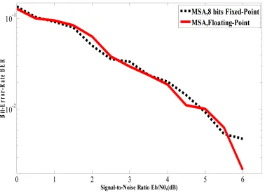
Figure 12 shows the BER (Bit-Error-Rate) versus SNR, obtained for the LDPC decoder from Matlab in floating and fixed point. One can clearly see the good agreement between the performances in term of the BER of the MSA algorithm in floating-point and 8 bits fixed-point representation.
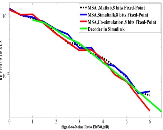
When comparing the MSA implementation both in Matlab, with VNPU and CNPU in the Matlab script managed Simulink and the designed VNPU in the Simulink associated to the VHDL CNPU modelization and the entire decoder designed in Simulink tool, we obtain quasi similar performances of the BER versus SNR evolution as shown on figure 13. The messages exchanged between the modules are all represented in 8 bits fixed-point two’s complement format.
6. Conclusion
In this paper we have proposed an efficient high level modular approach to design the VNPU and the CNPU blocks for the MSA. It uses Matlab, Simulink and ModelSim. The EDA Simulator Link for use with Mentor Graphic ModelSim is used to allow communication between hardware component and Simulink model. The proposed strategy yields great advantages in terms of design complexity and development time.
References
[1] Digital Video Broadcasting (DVB); Second generation framing structure, channel coding and modulation systems for Broadcasting, Interactive Services, News Gathering and other broadband satellite applications. Draft ETSI EN 302 307 V1.1.1 (2004-06). European Standard (Telecommunications series).
[2] Digital Video Broadcasting (DVB); Frame structure, channel coding and modulation systems for second generation digital terrestriel television broadcasting system (DVB-T2). Draft ETSI EN 302 755 V1.1.1 (2009- 09). European Standard (Telecommunications series).
[3] Gallager, R. G. (1963). Low Density Parity Check Codes, Cambridge, MA: MIT Press.
[4] Mackay, D. J. C. (1999). Good Error-Correcting Codes Based on very Sparse Matrices, IEEE Trans on Information Theory, 45 (2) 399-431.
[5] Fossorier, M. P. C., Mihaljevic, M., Imai, H. (1999). Reduced Complexity Iterative Decoding of Low Density Parity Check codes based on Belief Propagation, IEEE Trans.Commun, 47 (5) 673– 680.
[6] Chen, J., Dholakia, A., Eleftheriou, E., Fossier, M., Hu, Y. (2005). Reduced- Complexity Decoding of LDPC codes, IEEE Trans On Communications,53(8)1288-1299.
[7] Ait madi, A., Mansouri, A., Ahaitouf, A. (2012). Design,Simulation and Hardware implementation of Low Density Parity Check Decoders using Min-Sum Algorithm, IJCSI, 9 (3).