Q-bus-Product Overview
\ \.
r.
" "
Digital Equipment Corporation makes no representation that the interconnec-tion of its products in the manner described herein
will
not infringe on existing or future patent rights, nor do the descriptions contained herein imply the granting of license to make, use, or sell equipment constructed in accordance with this description.Digital believes the information in this publication is accurate as of its publica-tion date; such informapublica-tion is subject to change without notice. Digital is not responsible for any inadvertent errors.
The following are trademarks of Digital Equipment Corporation:
DATATRIEVE Letterwriter 100 RSX
DEC LSI RSX-ll
DECnet MicroPDP-11 RSX-11M-PLUS
DECProm MicroIbwerlPascal RX02
DECservice Micro/RSTS RX50
DECtape Micro/RSX RT -11
DIDOL Packetnet SB11
the Digital logo PDP SBC-ll/21
DSM -11 Professional ULTRIX
FMS Q-bus UNIDUS
FORTRAN IV
Rainbow
VAXlAS ReGIS VAXELN
Internet J-11
Letterprinter 100
RSTS RSTS/E
VMS VT
Contents
Part
I •
IntroductionChapter 1 • The Q·bus and Q·bus Modules
The Q-bus ... 1-1 Master/Slave Relationship ... 1-1 Device Registers and Addresses . . . .. 1-1 Interrupts and Device Priority ... 1-2 Q-bus Addressing ... 1-2 Q-bus Signal and Pin Identification . . . .. 1-3 Specifications . . . .. 1-13 Cabling and Cabinet Kits ... 1-16
Part
n •
MicrocomputersChapter 2 • Introduction to Microcomputers Chapter 3 • KDFll·AA LSI-11123 Microcomputer
Specifications . . . 3-1 Related Documentation . . . 3-2 Configuration. . . 3-2 Master Clock- WI ... 3-5 Event.Line- W4 ... 3-5 fbwerup Mode Selection- W5 and W6 ... 3-6 Haltffrap Option - W7 . . . 3-7 Starting Address 1730008 - W8 . . . 3-8
Chapter 4 •
KDFll-B LSI-1l/23-PLUS
MicrocomputerSpecifications . . . 4-2
Related Documentation . . . 4-2
Configuration. . . 4-3
Jumper and Switch Configuration . . . 4-3
Manufacturing Test Jumpers ... 4-5
CPU Option Jumpers ... 4-5
Ibwerup Mode Selection . . . 4-5
Haltlfrap Option-Jl6 ... 4-6
Onboard Device Selection Jumpers ... 4-7
Console SLU Switch and Jumper Configurations ... 4-9
BreaklHaltJumpers ... 4-10
Second SLU Switch and Jumper Configurations . . . 4-11
BootIDiagnostic Switches and Jumpers . . . 4-12
Q-bus Backplane Jumpers . . . 4-14
Cabinet Kits . . . 4-19
Chapter; •
KDJll-A LSI-UI73
MicrocomputerSpecifications ... 5-1
Related Documentation ... 5-1
Configuration ... 5-1
Ibwerup Options ... 5-3
Halt Option ... 5-4
Boot Address ... 5-4
Wakeup Disable ... 5-5
BEVNT Recognition ... 5-5
Chapter 6 •
KXTll-AB FALCON-PLUS SBe-11l21-PLUS
MicrocomputerChapter 7 • KXTll-CA Single-Board Computer
Specifications . . . 7-1
Related Documentation . . . 7-1
Configuration. . . 7-2
User EPROM,EEPROM, and ROM ... 7-5
Battery Backup. . . 7-6
User Socket
+
5V Ibwer . . . 7-6
Memory Maps . . . 7-6
Boot/Self-test Option. . . 7-8
Base Address . . . 7-9
Realtime Clock Interrupt . . . 7-10
Break Enable . . . 7-10
SLU 1 'fransmitter . . . 7-11
SLU 1 Receiver . . . .. 7-11
SLUI Baud Rate ... 7-11
DMA Requests. . . 7-12
SLU2 Channel A Receiver . . . 7-12
SLU2 Channel B Operation. . . 7-13
SLU2 Channel B Receiver .. . . 7-13
SLU2 Channel B 'fransmitter ... 7-14
Cables and Connectors ... 7-14
Parallel 110 Interface (J4) ... 7-14
Serial 110 Interfaces (J 1, }2, and}3) . . . 7-15
Loopback Connectors . . . 7-15
Part
m •
Memories
Chapter 8 • Introduction to Memories
Parity
Operation. . . 8-1
Wmdow Mapping ... 8-1
Refresh
Circuitry ... 8-2
Battery Backup. . . 8-2
Bootstrap ... " ... " 8-2
110 Jlage. . . . .. 8-2
Control and Status Registers ... 8-3
Chapter
9 •
MCVll-D CMOS ReadlWrite Memory with Battery Backup
Chapter 10 • MRVll·C Read·OnIy Memory Module
Specifications ... 10-1 Related Documentation . . . .. 10-2 Configuration ... 10-2 Direct Addressing Mode . . . .. 10-5 Wmdow-mapping Mode . . . .. 10-9 Bootstrap . . . .. 10-13 Use of Multiple MRV11-C Boards. . . .. 10-16 ROM Chips ... 10-17 Chip Access TIme. . . . .. 10-20 DATIO Bus Cycle Inhibit ... 10-20 Wrrewrap Pin Identification. . . .. 10-20
Chapter 11 • MRVll·D Universal Programmable Read.Only Memory
Specifications . . . .. 11-1 Relation Documentation ... 11-2 Configuration. . . . .. 11-2 Memory Array . . . .. 11-3 Addressing Modes . . . .. 11-10 Bootstrap . . . .. 11-13 Battery Backup Shunt ... 11-13 System Size Jumpers ... 11-14 DAID Bus Cycle ... 11-14 Read TIming. . . . .. 11-1'4 Installing the MXV11-B2 ROM ... 11-14
Chapter 12 • MSVll·D, ·E Dynamic MOS Readl\l1ite Memory
Specifications . . . .. 12-1 Related Documentation . . . .. 12-3 Configuration. . . .. 12 -3 Address Selection. . . .. 12 -3 Battery Backup Power ... 12-4 F'arity ... 12-4 Memory Size ... 12-5
Chapter 13 • MSVll·L MOS Random·Access Memory
Chapter 14 • MSVll-P MOS Random-Access Memory
Specifications . . . .. 14-1
Related Documentation . . . .. 14-2
Configuration. . . .. 14-3
Module Starting Address (MSA) ... 14-3
Control and Status Register (CSR)Jumpers ... 14-7
R>wer Jumpers. . . .. 14-8
Bus Grant Continuity Jumpers ... 14-9
Miscellaneous Jumpers ... 14-9
System Size Jumpers ... 14-9
Chapter 15 • MSVll-Q MOS Random-Access Memory
Specifications . . . .. 15-1
Related Documentation . . . .. 15-3
Configuration of the MSV11-QA (Etch Rev A) ... 15-3
Memory Starting and Ending Addresses . . . .. 15-5
Control and Status Register Address .... . . .. 15-8
Miscellaneous Jumpers. . . •. 15-8
Configuration of the MSVll-Q ... 15-9
Memory Starting and Ending Addresses .. . . ..
15~10
Control and Status Register Address ... 15-13
Battery Backup ... 15-14
Miscellaneous J wnpers ... , 15-15
Part IV •
Multifunction Modules
Chapter 16 • Introduction to Multifunction Modules
Chapter 17 • MXVll-A Memory and Asynchronous
Serial
Line Interface
Model Options. . . .. 17-1
Specifications . . . .. 17-1
Related Documentation . . . .. 17-2
Configuration. . . .. 17-2
Configuring
the
RAM ... 17-11
Configuring the ROM .. . . .. . . . .. 17-12
Chapter 18 • MXVll·B Multifunction Option Module
Specifications . . . .. 18-1 Related Documentation . . . .. 18-2 Configuration. . . .. 18-2 Configuring the RAM ... 18-4 ROM Configurations . . . .. 18-7 Configuring the Serial Line Units ... '. . .. 18-11 Linetime Clock. . . . .. . . .. 18-16 Master Clock . . . .. 18-17 MSVll-B2 ROM Set ... '" ... 18-17 Cables and Connectors ... 18-18
Part V • Asynchronous Communications Interfaces
Chapter 19 • Introduction to Asynchronous Communications Interfaces Chapter 20 • DHVll Asynchronous Multiplexer
Specifications . . . 20-1 Rdated Documentation ... 20-2 Configuration. . . 20-2 Address Switches . . . 20-3 Vector Switches ... 20-3 Bus Grant Continuity Jumpers ... 20-4 Cables and Cabinet Kits. . . 20-4 Null Modem Cables ... 20-5 Full Modem Cables ... 20-7 Data Rate to Cable Length Relationships . . . 20-8 Cabinet Kits . . . 20-8
Chapter 21· DLVll Asynchronous
Serial
Line UnitChapter 22 • DLVEI Asynchrono~ Line Interfate
Specifications ... 22-1 Related Documentation ... 22-1 Configuration ... 22-1 Register Addresses . . . 22 -5 Interrupt Vectors ... 22-7 Baud Rate Selection ... 22-7 Data Bit Selection ... 22-7 Cables and Cabinet Kits ... , 22-9
Chapter 23 • DLVJl Four-Channel Asynchronous Serial Interface
Specifications . . . 23-1 Related Documentation ... 23-1 Configuration ... 23-2 Device Registers ... 23-5 Interrupt Vectors ... 23-7 Character Fonnats ... 23-9 Baud Rates ... 23-10 Console Device Selection ... 23-11 Break Response .. . . 23-11 Peripheral Interface Configuration . . . 23-12 Cables and Cabinet Kits. . . 23-13
Chapter 24 • DZQll Asynchronous Multiplexer
Specifications . . . 24-1 Related Documentation . . . ... . . . 24-1 Configuration ... 24-1 Device Address ... 24-3 Vector Address ... 24-4
Test
Switch (E13-8) ... 24-5 Break Character Response ... 24-5 Modem Control ... 24-6 Baud Rate Jumpers ... 24-6 Cables, Connectors, and Cabinet Kits . . . 24-7Chapter 25 • DZVll Asynchronous Multiplexer
Chapter
26 • KMVll-AProgrammable Communications Controller
Specifications . . . 26-1 Related Documentation . . . 26-1 Configuration. . . 26-1 Device Address Switches . . . 26-3 Interrupt Vector Address Switches. . . 26-4 Self-test Switches . . . 26-4 Extended Address Jumpers ... 26-5 BOCOKJumper ... 26-5 Bus Continuity Jumpers ... 26-5 Factory Test Jumpers ... 26-5 Modem Signal Switches and Jumpers ... 26-5 Cables and Connectors ... 26-6
Part VI •
Synchronous Communications Interfaces
Chapter 27 • Introduction to Synchronous Communications Interfaces
DEQNA Ethernet Q-bus Network Controller ... 27-1 DMV11 Synchronous Controller ... 27-1 DPVll Serial Syncrhonous Line Interface. . . 27-1 DUVU Synchronous Line Interface ... 27-2 KMVll-A Programmable Communications Controller ... 27-2
Chapter 28 • DEQNA Ethemet Q-bus Network Adapter
Specifications . . . 28-1 Related Documentation ... 28-1 Configuration ... 28-2 Device Address Assignment (WI) ... 28-4 Bus Request Hold-off Tuner (W2) ... 28-4 Sanity Tuner (W3) ... 28-4 Cables and Cabinet Kits . . . 28-4
Chapter 29 • DMVII Synchronous Controler
Chapter 30 - DPVll Serial Synchronous Line Interface
Specifications . . . 30-1 Related Documentation . . . 30-2 Configuration. . . 30-2 Device Address ... 30-4 Interrupt Vector Address . . . 30-4 Drive AttentuationJumper ... 30-5 Interface Selection Jumpers . . . 30-5 Receiver Termination Jumpers . . . 30-6 Clock Jumpers . . . 30-6 Data Set Jumpers . . . 30-6 Cables and Cabinet Kits. . . 30-7
Chapter 31- DUVII Line Interface
Specifications . . . 31-1 Related Documentation . . . 31-1 Configuration. . . 31-1 Device Address ... '... 31-2 Interrupt Vector Address . . . 31-4 Option Switches '. . . . 31-4 Cables ... 31-5
Part VB - Analog Interfaces
Chapter 32 - Introduction to Analog Interfaces Chapter 33 - AAVll-C Analog Output Board
Specifications ... 33-1 Related Documentation ... 33-2 Configuration ... 33-2 Device Address ... 33-2 Output Voltage Range Selection. . . . 33-4 Interfacing to the AAV ll-C ... , . . . 33 -5
Chapter 34 - ADVll-C Analog-to-Digital Converter
Interfacing to the ADVll-C ... 34-7
Single-Ended Inputs (16 Channels) ... 34-7
Pseudo-Differential Inputs (16 Channels) ... 34-8
Differential Inputs (8 Channels) ... 34-9
Chapter 35 • AXVll-C Analog Input/Output
Board
Specifications ... 35-1
Related Documentation . . . 35-3
Configuration ... 35-3
Device Address ... 35-5
Interrupt Vector Address ... 35-6
Analog Input Range, Type, and Iblarity ... 35-6
AID Output Data Notation ... 35-7
Externallligger Source . . . 35-7
DI A Configuration ... 35-8
Interfacing to the AXVll-C ... 35-9
Chapter 36 • KWVll-C Programmable Realtime Oock
Specifications . . . 36-1
Related Documentation ... 36-2
Configuration. . . 36-3
Device Address ... 36-5
Interrupt Vector Address . . . 36-5
Schmitt lligger Reference Levels and Slopes . . . 36-6
External
Control of Schmitt 1Hggers . . . .. . . .. . . .. 36-7
Interfacing to the KWVll-C ... 36-7
Part
vm •
Paralld Interfaces
Chapter 37 • Introduction to Parallel Interfaces
DRVll Parallel Line Unit ... 37-1
DRVll-] High-Density Parallel Interface ... ' ... 37-1
DRVll-WA General Purpose DMA Interface ... 37-1
IBVll-A Instrument Bus Interface ... 37-1
IEQll·A DMA IECIIEEE Bus Interface Option ... 37-2
Chapter 38 • DRVll Parallel Line Unit
Configuration. . . 38-1
Device Address ... 38-3
Interrupt Vector Address . . . 38-3
NEW DATA RDY and DATA TRANS Pulse Width Modification ... 38-4
Cables and Cabinet
Kits. . . ..38-4
Chapter 39 •
DRVll-J
High-Density
Parallel
Interface
Specifications . . . 39-1
Related Documentation . . . 39-2
Configuration. . . 39-2
Device Address ... 39-4
Interrupt Vector Address ... 39-5
Cables and Cabinet
Kits . . .39-6
Chapter 40 •
DRVll-WA
General Purpose
DMA
Interface
Specifications . . . .. 40-1
Related Documentation . . .40-2
Configuration. . . 40-2
Device Address ... 40-2
Interrupt Vector Address . . . 40-3
Addressing Mode. . . 40-4
Cables and Cabinet
Kits . . .40-4
Chapter 41 •
mVll-A
Instrument Bus Interface
Specifications . . . .. 41-1
Related Documentation . . . 41-1
Configuration. . . .. 41-1
Device Address ... 41-3
Interrupt Vectors ... 41-4
Cables and Connectors ... 41-5
Optional Cables . . . 41-7
Chapter 42 •
IEQll-A DMA
Interface Option
Part
IX •
Peripheral Interfaces
Chapter 43 • Introduction to Peripheral Interfaces
LPVll Printer Option ... 43-1 RLV12 Disk Controller ... 43-1 RQC25 Disk Controller ... " ... 43-1 RQDXl Disk Controller . . . 43-1 RXV21 Floppy Disk Option ... . . 43-2 TQK25 Streaming Tape Drive Interface ... 43-2 TSV05 Tape 'fransport Subsystem ... 43-2 11158 Cartridge Tape Drive ... 43-2
Chapter 44 • LPVll Printer Option
Specifications . . . 44-1 Related Documentation . . . 44-2 Configuration. . . . 44-2 Device Address ... 44-5 Interrupt Vector . . . 44-5 Bus Reply Tuning. . . 44-6 Uppercase Only . . . .. 44-6 Farity ... 44-6 Error Filter. . . 44-7 Cables ... 44-7
Chapter 45 • RLVU Disk Controller
Specifications . . . 45-1 Related Documentation ... 45-2 Configuration ... 45-2 Device Address Selection ... 45-3 Bus Selection ... 45-7 Interrupt Vector ... 45-7 Interrupt Request Level ... 45-8 Memory Farity Error Abort Feature ... 45-8 Jumpers That Remain Installed .. . . 45-8 Cables and Cabinet Kits ... 45-9
Chapter 46 • RQC25 Adapter Module
Chapter 47 • RQDXl Disk Drive Controller
Specifications . . . 47-1
Related Documentation . . . 47-4
Configuration. . . 47-4
Device Address Selection ... 47-5
Logical Unit Number Selection ... 47-6
Interrupt Vector ... 47-7
RQDXI-E Extender Module Option ... 47-7
Configuration ... 47-7
Cables and Cabinet Kits . . . 47-9
Chapter 48 • RXV21 Floppy Disk Option
Specifications . . . 48-1
Related Documentation . . . • . . . 48-3
Configuration. . . .. 48-4
Cables and Cabinet Kits. . . 48-6
Chapter 49 • TQK2;
TapeDrive Adapter Module
Specifications . . . 49-1
Related Documentation . . . 49-1
Configuration ... : . . . 49-1
Device Address ... 49-4
Interrupt Vector Address ... 49-5
Block Mode DMA ... 49-5
Q-bus Address Mode ... 49-5
Interrupt Priority Level .. . . 49-6
Cables and Cabinet Kits. . . 49-6
Chapter ;0 • TSVO;
Tape'&ansport Subsystem
Chapter 51 • TU58 Cartridge
Tape
Drive
Specifications . . . 51-1
Related Documentation . . . 51-3
Configuration. . . 51-3
Part X •
Backplanes, Enclosures,
and
Expansion Cables
Chapter 52 • Introduction to Backplanes, Enclosures, and Expansion
Backplanes ... 52-1
Enclosures ... 52-2
Bus Termination ... 52-3
Expansion Cables. . . . 52-4
Chapter 53 • BAll·M Enclosure
Specifications ... 53-1
Related Documentaiton ... 53-2
Description ... 53-2
Cables ... 53-4
Chapter 54· BAll·N Enclosure
Specifications . . . 54-1
Related Documentation . . . 54-2
Description and Configuration. . . 54-3
Backplane Configuration ... " . . . 54-4
Bezel Assembly Jumpers ... 54-4
Chapter 55· BAll·S Enclosure
Specifications ... 55-1
Related Documentation ... 55-3
Configuration. . . 55 -3
Chapter 56 • BA23·A Enclosure
Chapter ;7 • DDVU-B Backplane
Description and Specifications. . . 57-1
Related Documentation ... 57-2
Configuration. . . 57-2
Module Slot Assignments ... 57-2
dc Ibwer and Ibwer Signal Connections ... 57-4
Chapter 58 • H780 Power Supply
Specifications ... 58-1
Notes Relating to Specifications ... 58-3
Related Documentation ... 58-3
Description ... 58-4
Console Controls and Indicators . . . 58-4
+
12 V and
+
5 V Adjustment Procedure . . . 58-4
Chapter 59 • H9270-Q Backplane
Specifications . . . 59-1
Configuration. . . 59-2
Mounting the Backplane ... 59-3
dc Ibwer Connections ... 59-5
Chapter 60 • H9273-A Backplane
Specifications . . . 60-1
Related Documentation . . . 60-1
Configuration. . . 60-1
Chapter 61 • H9275-A Backplane
Specifications . . . .. 61-1
Related Documentation . . . 61-2
Configuration. . . .. 61-2
Connecting System Ibwer .. . . .. 61-3
ConnectingConttol Bus Signals ... 61-4
Bus Priority ... 61-5
Bus Termination. . . .. 61-6
Bus Restrictions . . . .. 61-6
Chapter 62 • H9281-Q Backplane
Device Priority. . . 62-6
Bus Terminations ... 62-6
16- and 18-Bit Addressing ... 62-6
Chapter 63 • TEVll Terminator
Specifications . . . .. 63-1
Related Documentation . . . 63-1
Description ... 63-1
Appendix A • Chip Kits
DC003 Interrupt Chip ...
A-2
DCOO4 Protocol Chip ...
A-2
DCOO51i-ansceiver Chip ...
A-3
OCOO6 \Xbrd CountlBus Address Chip ... A-3
DCOIO Direct Memory Access Chip ...
A-4
Related Documentation ... A-4
Appendix B • System Configuration Concepts
Configuration Steps ... B-1
Configuration Rules ... B-2
Configuring Single Backplane Systems ... B-3
Configuring Multiple Backplane Systems ... B-3
Example ... B-3
Problem Statement ... B-4
Block Diagram ... B-4
Processing and Software Requirements ... B-4
Hardware Product Selection ... B-5
Backplane and Ibwer Supply ... B-6
Cables and Cabinet Kits ... B-7
Appendix C • Mature Q-bus Products
.
Foreword
This
handbook is a reference guide for board-level microcomputers, memories, interfaces, and peripheral options that can be installed on the Q-bus. The book is divided into ten parts (listed below) and three appendixes.• Hut I: Introduction
• Hut II: Microcomputers • Hut
m:
Memories• Hut IV: Multifunction Modules
• Hut
V: Asynchronous Communications Interfaces • Hut VI: Synchronous Communications Interfaces• Hut VII: Analog Interfaces • Hut VIII: Parallel Interfaces • Hut IX: Peripheral Interfaces
• Hut
X: Backplanes, Enclosures, and Expansion CablesWithin P.nts
II through IX each module isdiscussed
separately in an individual chapter .. Following a brief description of the module, each chapter includes specification, configuration, and (where appropriate) cabling and cabinet kit information. The appendixes provide related information on configuration of a Q-bus system, on modules that are no longer marketed, and on chip kits. For more information on configuring Q-bus systems including summarycharts
Chapter
1 •
The Q-bus and Q-bus Modules
• TheQ-bus
System components, including the processor, memory, and peripherals, are interconnected and communicate with each other via the Q-bus. The form of communication is the same for all devices on the bus; instructions that commu-nicate with memory can commucommu-nicate with peripheral devices. Each device, including memory locations and peripheral device registers, is assigned an indi-vidual byte or word address on the bus.
Master/Slave Relationship
Communication between devices on the bus is asynchronous. A master/slave relationship exists throughout each bus transaction. At any time, there is one device that has control of the bus. This controlling device is known as the bus master. The master device controls the bus while communicating with another device, known as the slave. The bus master (typically the processor or a direct memory access [DMA] device) initiates a bus transaction. The slave device responds by acknowledging the transaction in progress and by receiving data from, or transmitting data to, the bus master. Q-bus .control signals transmitted or received by the bus master or slave device must complete the sequence according to bus protocol. Thble 1-1 lists signals.
The processor controls bus arbitration, determining which device becomes bus master at any given time. A typical example of this relationship is the processor, as master, fetching an instruction from memory, which is always a slave. Com-munication on the Q-bus is interlocked so that for certain control signals issued by the master device, there must be a response from the slave in order to com-plete the transfer. It is
this
master/slave signal protocol that makes the Q-bus asynchronous. The asynchronous operation precludes the need for synchro-nizing with, and waiting for,clock
pulses.Device Registers and Addresses
1-2 • The Q-bus and Q-bus Modules
~ripheral device addresses within the
va
page are decoded by each device itself. Each peripheral includes one or more device registers, accessible under program control in exactly the same manner as memory locations. These regis-ters (generally known as control and status regisregis-ters, or CSRs) contain all the necessary information to establish communications with the device. Additional data buffer registers (DBRs) are used for temporary storage of data to be trans-ferred into and out of the processor.Interrupts and Device Priority
The interrupt capability of the Q-bus allows any
va
device to temporarily sus-pend (or interrupt) current program execution and divert processor operation to service the requesting device. Interrupts can be caused by devices connected to the Q-bus or by actions within the CPU itself. Those interrupts that originate within the CPU are called trapsand
are caused by programming errors, hard-ware errors, special instructions, or maintenance features.When an interrupt request is received from the bus, the processor completes execution of the present instruction, saves the program counter (PC) and processor status (PS) words on the stack and acknowledges the interrupt.
The
highest priority device requesting interrupt service responds by inputting its interrupt vector address to the processor. The processor uses this vector address as a pointer to two memory locations containing the starting address (PC) and processor status (PS) of the device's internIpt service routine. Program control is transferred to the service routine. Once the service routine has com-pleted execution, control is either returned to
the
previously interrupted pro-gram or transferred tothe
service routine of the next device requestmg interrupt service.The Q-bus supports the following two methods of establishing device priority: • Distributed arbitration - priority levels are implemented on the hardware. When devices of an equal priority
level
request an interrupt, priority is given to the device electrically closest to the processor.• Ibsition-defined arbitration - priority is determined solely by electricalposi-don on the bus. The closer a device is to the processor, the higher its J>riority.
Q-bus Addressing
1-3
As
mentioned above,all
peripheral device addresses are located within the 110 page, regardless of the addressing mode of the bus. When the 110 page is addressed, the processor must assert the "bank 7 select" (BBS7) bus signal. All peripheral devices use this signal line during addressing rather than decoding the upper address bits.An
asserted BBS7 signal always indicates an address in the 110 page, thereby enabling peripheral device addressing.It should be noted, however, that memories or 110 devices that are not capable of 22-bit addressing can generate or decode erroneous addresses
if
they are used in systems that implement 22-bit addressing. Such devices can be used in a 22-bit system onlyif
the size of the system is restricted to the address range of the device.For more detailed information on the Q-bus, refer to the
PDP-II Architedure
Handbook.
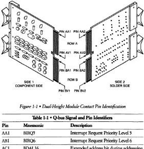
Q-bus Signal and Pin Identification
The Q-bus is based on the use of dual-height modules that plug into a 2-s10t bus connector. Each slot contains 361ines-18 each on the component and solder sides of the circuit board - making a total of72 contact pins carrying 72 individ-ual signals. These contact pins are identified in the following fashion:
• The two slots are designated A or B-matching rows A and B on the module (as shown in Figure 1-1).
• The component side of the module is designated side 1 and the solder side is designated side 2.
• The 18 pins on each side of each slot (or row) are identified using letters A through V (excluding G, I, 0, and Q).
An
actual pin identifier has the format "slot/pin/side." For example, pin AAI is the first pin of slot A, side 1; pin BF2 is the fifth pin of slot B, side 2; and pin BVI is the eighteenth pin of slot B, side 1.1-4 • The Q-bus and Q-bus Modules
Pin
AAl
ABl
ACl
ADl
SIDE 1
COMPONENT SIDE
l
PIN BV1
[image:30.380.52.333.58.349.2]SIDE 2 SOLDER SIDE
Figure
1-1 •Dual-Height Module Contact Pin Identification
Table 1-1 • Q-bus Signal and Pin Identifiers
Mnemonic BIRQ5 BIRQ6 BDAL16
BDAL17
Description
Interrupt Request Priority Level 5
Interrupt Request Priority Level 6
Extended address bit during addressing protocol; memory error data line during data transfer protocol
Extended address bit during addressing protocol; memory error logic enable during data transfer protocol
1-5
Table 1-1 • Q-bus Signal and Pin Identifiers (Cont.)
Pin
Mnemonic
Description
AEI SSPAREI Special Spare- not assigned or bused (Alt<!rnate
+
5B) in Digital cable or backplaneassem-blies; available for user connection. Optionally, this pin can be used for
+
5 V battery (+
5B) backup power to keep critical circuits alive during power fail-ures. A jumper is required on Q-bus options to open (disconnect) the+
5B circuit in systems that use this line as SSPAREI.AFI SSPARE2 Special Spare- not assigned or bused in Digital cable or backplane assem-blies; available for user connection. In the highest-priority device slot, the processor can use this pin for a signal to indicate its RUN state.
AHI SSPARE3 and SRUN Special Spare-not assigned or bused (simultaneously) in Digital cable or backplane
assem-blies; available for user connection. An alternate SRUN signal can be connected in the highest-priority slot.
A]I GND Ground - System signal ground and dc
return
AKI MSPAREA Maintenance Spares- normally con-ALl MSPAREB nected together on the backplane at each option location (not a bused con-nection)
AMI GND Ground - System signal ground and dc
return
1-6 • The Q-bus and Q-bus Modules
Pin
ANI
API
ARI
Table I-I • Q-bus Signal and Pin Identifiers (Cont.)
Mnemonic BDMR
BHALT
BREF
Description
Direct Memory Access (DMA) Request - A device asserts this signal to request bus mastership. The processor arbi-trates bus mastership between itself and
all
DMA devices on the bus.If
the processor is not bus master (it has com-pleted a bus cycle and BSYNC is not being asserted by the processor), it grants bus mastership to the requesting device by asserting BDMGO. The device responds by negating BDMR and asserting BSACK.Processor Halt - When BHALT is asserted for at least 25 microseconds, the processor services the halt interrupt and responds by halting nonnal pro-gram execution. External interrupts are ignored but memory refresh interrupts in the LSI-II are enabled if W 4 on the M7264 and M7264-YA processor mod-ules is removed and DMA request! grant sequences are enabled. The processor executes the ODT microcode and the console device operation is invoked. Memory Refresh - Asserted by a DMA device. This signal forces
all
dynamic MOS memory units requiring bus refresh signals to be activated for each BSYNCIBDIN bus transaction. It is also used as a control signal for block mode DMA.Note
The user must avoid multiple DMA data transfers (burst or "hog" mode) that could delay refresh operation if using DMA refresh. Complete refresh cycles must occur once every 1.6 milliseconds
if
required.Pin
ASI ATI AUI AVI BAI BBI BCl BDI BEl BFI 1-7Table 1-1 • Q-bus Signal and Pin Identifiers (Cont.)
Mnemonic
+ l2B or +5B
GND PSPAREI +5B BDCOK BPOK SSPARE4/BDAL18 SSPARE5/BDAL19 SSPARE6/BDAL20 SSPARE7/BDAL21
Description
+ 12
V
dc or + 5V
Battery Backup Power to keep critical circuits alive dur-ing power failures. This signal is not bused to BS 1 inall
Digital backplanes. A jumper is required onall
Q-bus options to open (disconnect) the backup circuit from the bus in systems that use this line at the alternate voltage. Ground - System signal ground and dc returnSpare-not assigned; customer usage not recommended. Prevents damage when modules are inserted upside down.
+
5 V Battery fuwer- Secondary + 5 V power connection. Battery power can be used with certain devices.dc Power OK - Power supply-generated signal that is asserted when there is suf-ficient dc voltage available to sustain reliable system operation.
fuwer OK-Asserted by the power sup-ply 70 milliseconds after BneOK is negated when ac power drops below the value required to sustain power (approximately 75 percent of nominal). When BPOK is negated during proces-sor operation, a powerfail trap sequence is initiated.
Special Spares (in l8-bit Q-bus) - Not assigned. Bused in 22-bit cable and backplane assemblies; available for user connection. (Caution: These pins may be used as test points by Digital in some options.)
Address Lines <21: 18> (in 22-bit Q-bus). Currently not used during data transfers.
1-8 • The Q-bus and Q-bus Modules
Table
I-I •
Q-bus Signal
and
PinIdentifiers
(Cont.)
Pin
Mnemonic
Description
BHl SSPAREB Special Spare- Not assigned or bused in Digital cable and backplane assem-blies; available for user connection.
BJI GND Ground - System signal ground and dc
return
BKl MSPAREB Maintenance Spares- Normally con-BLI MSPAREB nected together on the backplane at
each option location (not a bused con-nection).
BMl GND Ground - System signal ground and dc
return
BNl BSACK This signal is asserted by a DMA device in response to the processor's BDMGO signal, indicating that the DMA is bus master.
BPI BIRQ7 Interrupt Request Priority
Level
7 BRI BEVNT External Event InterruptRequest-When this signal is asserted, the proces-sor responds by entering a service rou-tine via vector address 100. A typical use of this signal is a linetime clock interrupt.
BSI +12B + 12 V dc Battery Backup Ibwer- not
bused to AS 1 in
all
Digital backplanesBTl GND Ground - System signal ground and dc
return
BUI PSPARE2 Spare- Not assigned; customer usage is not recommended. If a module is using
- 12 V (on pin AB2) and if the module is accidentally inserted upside down in the backplane, - 12 V dc appears on this pin.
BVI +5V
+
5 V Ibwer- Normal + 5 V dc systempower
AA2 +5V
+
5 V Ibwer- Normal + 5 V dc systempower
Pin
AB2 AC2 AD2 AF2 AF2 AH2 1-9Table 1-1 • Q-bus Signal and Pin Identifiers (Cont.)
Mnemonic -12V
Description
- 12 V Power- Optional - 12 V dc power for devices requiring this voltage Note
LSI-II modules that require negative voltages contain an inverter circuit (on the module) which generates the required voltages. Hence, -12 V power is not required with Digital-supplied options. GND +12V BOOUT BRPLY BDIN
Ground - System signal ground and dc return
+
12 V Power- 12 V dc system power Data Output - When asserted, BOOUT implies that valid data is available on BDAL <0:15> and that an output transfer, from the bus master device, is taking place. BOOUT is deskewed with respect to data on the bus. The slave device responding to the BOOUT signal must assert BRPLY to complete the transfer.Reply-BRPLY is asserted in response to BDIN or BOOUT and during IAK trans-actions.
It
is generated by a slave device to indicate that it has placed its data on the BDAL bus or that it has accepted output data from the bus.Data Input- Used for two types of bus operations.
When asserted at the same time as BSYNC, BDIN signals an input transfer to the current bus master and requires a response (BRPLY). The master device must deskew input data from BRPLY. When asserted without BSYNC, BDIN signals an interrupt operation.
1-10 • The Q-bus and Q-bus Modules
Table I-I • Q-bus Signal and Pin Identifiers (Cont.)
Pin
AJ2 AK2 AU AM2 AN2Mnemonic
BSYNC BWTBT BIRQ4 BIAKI BIAKODescription
Synchronize - BSYNC is asserted by the bus master device to indicate that it has placed an address on BDAL<O: 17>. The transfer continues until BSYNC is negated.
WritelByte-BWTBT is used in two ways to control a bus cycle: It is asserted at the leading edge of BSYNC to indicate that an output sequence (rather than an input sequence) is to follow.
It is asserted during BOOUT (in a DAIDB bus cycle) for byte addressing. Interrupt Request Priority Level 4 - A level 4 device asserts this signal when its interrupt enable and interrupt request flip-flops are set.
If
PS<7> is 0, the processor acknowledges the request by asserting BDIN and BIAKO.Interrupt Acknowledge - In accor-dance with interrupt protocol, the processor asserts BIAKO to acknowl-edge receipt of an interrupt. The bus transmits this to BIAKI of the device electrically closest to the processor. This device accepts the interrupt acknowl-edge under two conditions:
( 1) The device requested the bus by asserting BIRQx, and (2) the device has the highest-priority interrupt request on the bus at that time.
If
these conditions are not met, the device asserts BIAKO to the next device on the bus. This process continues in a daisychain fashion until the device with the highest interrupt priority receives the interrupt acknowledge signal.1-11
Table 1-1 • Q-bus Signal and Pin Identifiers (Cont.)
Pin
Mnemonic
Description
AP2 BBS7 Bank 7 Select - The bus master asserts this signal to reference the 110 page (including that portion of the 110 page reselVed for nonexistent memory). The address in BDAL <0: 12> is the address
within
the 110 page.AR2 BDMGI Direct Memory Access Grant - The
AS2 BDMGO bus arbitrator asserts this signal to grant bus mastership to a requesting device, according to bus mastership protocol. The signal is passed from the arbitrator (as BDMGO), through the bus, to BDMGI of the device electrically closest to the processor. This device accepts the grant only if it requested the bus by asserting BDMR If not, the device passes the grant to the next device on the bus. The process continues until the requesting device acknowledges the grant.
AT2 BINIT Initialize- This signal is used for system reset. When BINIT is asserted, all devices on the bus are required to return to a known, initial state (i.e., all registers and logic are set to zero). Any exceptions should be completely docu-mented in programming and engineer-ing specifications for the device. AU2 BDALO Datal Address Lines - These two lines AV2 BDAL1 are part of the 16-line dataladdress bus
over which address and data informa-tion are passed. (See BDAI2 through BDAL15.)
BA2 +5V + 5 V Power- Normal + 5 V dc system
power
BB2 -12V -12 V Power-Optional -12 Vdc
1-12 • The Q-bus and Q-bus Modules
Thble
1-1 •Q-bus Signal and Pin Identifiers (Cont.)
Pin
Mnemonic DescriptionBC2 GND Ground - System signal ground and dc
return
BD2 +12V + 12 V Ibwer-12 V dc system power
BEl
BDAl2 Data/ Address Lines - These 14 lines BF2 BDAL3 are part of the 16-line data/address bus BH2 BDAL4 over which address and data informa-BJ2 BDAL5 tion are passed. Address information is BK2 BDAL6 first placed on the bus by the bus BI2 BDAL7 master device. The same bus lines are BM2 BDALB then used for the actual data transfer. BN2BP2 BR2 BS2 BT2 BU2 BV2
BDAL9 BDALlO BDALll BDAL12 BDAL13 BDAL14 BDAL15
Note
1-13
• Specifications
Individual module specifications are included in each module chapter. These specifications include (at least) the following characteristics:
• Identification
The module identification is the number assigned to each module. This num-ber is printed on the module handle and can be used as a quick reference to determine what specific options are installed in a given system.
• Size
Q-bus-compatible modules are standardized as either dual- or quad-height modules. The standard dimensions for each size module (shown in Figure 1-2) are as follows:
Dual: 13.2 cm (5.2 in) high 22.8 cm (8.9 in) long 1.27 cm (0.5 in) thick Quad: 26.5 cm (10.5 in) high 22.8 cm (8.9 in) long
1.27 cm (0.5 in) thick • Ibwer Requirements
The power requirements specify the power used by the option when con-nected to the Q-bus backplane. These requirements are used to determine the total power supply loading within a single system.
• Bus Loads
5.187+.018
:-1
10.457+.015(DOUBLE'~~T.)
(QUADH~?P.)
.18 . 0 0 0 _
NOTES:
DIMENSIONS GIVEN IN INCHES DIMENSIONS DENOTED BY • ARE FOR MAX. USEABLE CIRCUIT AREA
. 219 1
5.250~
±.010--l
~
±.01O°Wt1
-tj+
+1+
+11
~
f~:~
HANDl
HOL~
~
100m.UNLESS OTHERWISE SPECIFIED ALL DIMENSIONS ARE ± .005 in
, 8.430±·01O
(EXT. LGTH.) ••
.156 ±.01O
2.312· (SINGLE HGT.)
\
7.438· (EXT. LGTH.)
-4,---...:..+-+~- +
I
+ + +---I----:!:.
5.062·I+----~(DOUBLE HGT.)--l 10.312·
I+---.jl---+--(QUAD. HGT.) I .1
3.938· (STD. LGTH.)
2.125 TYP. (17 EQUAL SPACES)
FiQure
1-2 •O-bus Module Dimensions
BOTTOM OF FINGERS TO TOP OF HANDLE 8.94±·01O (EXT. LGTH.) 5.50±·010 (STD. LGTH.)
.1-15
Most Q-bus modules are designed to operate within the environmental specifications listed in 'Thble 1-2. Any module characteristics that do not meer or that exceed this ret of specifications are listed in the individual mod-ule chapters.
Thble 1-2 • Q-bus Environmental Specifications
Temperature Storage Operating
-40°C to 66°C (-40°F to 150°F) 5°C to 60°C (41°F to 140°F) Note
The module must be brought into the operating environment and be allow~d to stabilize at the operating temperature for a mini-mum of 5 minutes before operating.
Relative Humidity
Storage Operating
Wet bulb temperature Dew point
Altitude Storage Operating
10% to 90%, noncondensing 10% to 90%, noncondensing 28°C (82°F) maximum 2°C (36°F) minimum
Up to 15 km (50,000 ft) Up to 15 km (50,000 ft) (90 mm mercury minimum) Note
Lower the maximum operating temperature by one Celsius degree (1.8 Fahrenheit degrees) for each 305 m (1,000 ft) of altitude above 2.4 km (8,000 ft).
Air
Quality
Air must be noncaustic.1-16 • The Q-bus and Q-bus Modules
18ble 1·2 • Q·bus Environmental SpeCifications (Cont.)
Airflow (operating) There must
be
enough airflow to limit the input to output temperature rise across the module to five Celsius degrees (nine Fahrenheit degrees) when the input temperature is 60°C (140°F).For operation below 55°C (131°F), there must be enough airflow to limit the input to output temperature rise across the module to 10 Celsius degrees (18 Fahrenheit degrees)
maximum.
Note
These are design limits. Lower temperature limits
will
help increase the life of the module.• Cabling and Cabinet Kits
Digital has implemented a design for shielding cabinets and cabling to reduce the potential of electromagnetic interference from computer devices. This new system is made up of three parts:
• A shielded CPU enclosure and an internal cable that originates at the option module or controller.
• A shielded 110 connection panel that joins the internal and external cables and provides the transition between option modules and externally con-nected devices.
• An
external cable that attaches to the peripherals.The 110 connection panel completes the shielding envelope and provides the filtering necessary to contain potential radio frequency interference within the cabinet. All cables entering or exiting the cabinet must do so via the I/O connec-tion panel. (See Figure 1-3.)
SHIELDED CABINET AND CABLING
SHIELDED CPU ENCLOSURE
OPTION CONNECTION PANEL INSERTS
1-17
LJ:::JJ:======:S;::..u }
I/O CONNECTION PANELPOWER CONTROLLER
Chapter 2 • Introduction to Microcomputers
The Digital Q-bus microcomputer family consists of a set of compatible proces-sors that use a common architecture and a common instruction set. These processors are connected to the Q-bus backplane as a subsystem that executes programs and arbitrates usage of the Q-bus for peripherals.
Note
The KXTll-CA is unique among the processors listed here. While it implements the Q-bus specifications as a bus slave, it is incapa-ble of arbitrating the bus. As a DMA device, however, it can become bus master to transfer data when the arbiter grants the bus.
In
this
mode it serves as an intelligent peripheral or as an 110 processor module (lOP). It can also be used as a single-board com-puter (SBC) in a stand-alone fashion.Features common to all Q-bus microcomputers include the following: • The PDP-11 instruction set, providing powerful and convenient
programming.
• Direct addressing of 16-bit words or 8-bit bytes, providing flexibility in defin-ing data structures.
• Twelve addressing modes for specifying operands, permitting absolute, deferred, autoincrement, autodecrement, and index register references. • Six general purpose and two special purpose internal registers for use as
accu-mulators and for operand addressing, providing flexible programming techniques.
• Stack processing, providing convenient handling of structured data, subrou-tines, and interrupts.
• Byte-oriented instructions, permitting efficient processing of 8-bit characters without the need to rotate, swap, or mask.
• Q-bus interface, allowing communication with all Q-bus compatible products.
2-2 • Introduction to Microcomputers
• Vectored interrupts, providing fast interrupt response without device polling. • Ibwerfaillautorestart hardware that detects and protects against ac power
fluctuations.
• Compact, modular component design, providing versatile packaging and allowing systems to be configured and upgraded easily.
• Asynchronous bus operation, allowing processor and system components (memory and peripherals) to run at their highest possible speeds.
Additional features available on sdected Q-bus microcomputers include the following:
• anT
console emulator, providing ease of debugging.• Recognition of memory parity errors during every data-in bus cycle providing overall system integrity.
• The extended integer instruction set (EIS) and the floating-point instruction set (FPll on processors such as the KDJll-A or the KDFll with KEFll), pro-viding fixed and floating-point hardware arithmetic.
• Multilevd interrupt bus structure, allowing the priority of bus operation for each levd to be conveniently determined by their physical locations on the bus.
• Extended addressing to support more users per system and provide increased system performance.
• Memory management, allowing rdocation and protection needed in mul-titask environments.
• Built-in expansion capability, eliminating the need for an expander box. • Line-frequency clock, providing the system with timing information at fixed
intetvals.
• Ibwerup self-test diagnostics to provide assurance of proper module operation.
See the
PDP-11 Architecture Handbook
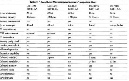
for a detailed discussion of these and other features.Table 2-1 • Board-Level Microcomputer Summary/Comparison Chart
LSI· 11/23 LSI· 11/23
+
LSI· 11173 FALCON + I/OPROCKDF11-AA KOFll-BA KPJll-AA KXT11·AB KXT11-CA
Q-bus addressing 22-bit 22-bit 22-bit 16-bit 22·bit
Memory capacity 4 Mbytes 4 Mbytes 4 Mbytes 64 Kbytes 64 Kbytes
Memory management yes yes yes no no
Q-bus interrupts 4-level 4-level 4·level I-level not applicable
FIS instruction set no no no no no
FP 11 instruction set optional optional yes no no
EIS instructions yes yes yes no no
Memory parity check yes yes yes no no
Line-frequency clock no yes no yes yes
Self-test diagnostics no yes no no yes
Expansion capability yes yes yes yes no
Onboard serial I/O no 2 ports no 2 ports 3 ports
Onboard parallel I/O no no no 24-line 20-line
Onboard memory no no no yes yes
Onboard cache no no yes no no
OOT microcode yes yes yes no no
OOT firmware no no no yes yes N
[image:49.577.81.520.55.330.2]Chapter 3 • KDFll-AA LSI-11/23 Microcomputer
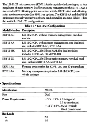
The LSI-11/23 microcomputer (KDF11-AA) is capable of addressing up to four megabytes of main memory.
It
offers memory management (the KTF11-AA), a microcoded FPll point instruction set (the KEFll-AA) , and a floating-point accelerator module (the FPF11) as options. The KEF11-AA and the FPF 11 options are mutually exclusive; only one can be installed at a time. Thble 3 -lUsts the available LSI-H/23 configurations.Model Number
KDFI1-AC
KDFll-AA
KDFll-HI<
KDFll-LK
KEFll-AA
KTFll-AA
• Specifications
Identification
Size
Table 3-1 • LSI-11l23
ConfigurationsDescription
LSI-11123 CPU without memory management, one dual module
LSI-ll/23 CPU with memory management, one dual mod-ule; includes KDFll-AC, KTFll-AA
LSI-ll/23 CPU, 256-Kbyte RAM, five dual modules; includes KDFll-AA, (4) MSVll-DD
LSI-ll/23 CPU, 256-Kbyte parity memory, two dual mod-ules; includes KDFll-AA, MSVll-LK
Floating-point option for KDF11-AA, one 40-pin package
Memory management option for LSI-11/23 CPU, one 40-pin package
M8186
Dual
Power Requirements
+
5 V ± 5%,2.0 A (typical)Bus Loads ac dc
3.2 A (maximum)
+
12 V ±5%, 0.2 A (typical)2.0 1.0
[image:51.381.41.326.93.492.2]3-2 • KDF11-AA LSI-11123
Microcomputer
Performance*
Worst Case
Typical
Interrupt SeIVice Tnne DMALatency
55.7 microseconds (for infrequently used instructions); 10.8 microseconds (for more frequently used group) 6.0 microseconds
8.2 microseconds
3.49 microseconds (worst case) *Tuning (Based on 300-nanosecond CPU microcyde time)
Interrupt Latency (based on MSV II-D without parity, add 500 ns worst case with parity)
• Related Documentation
Document TItle
KDFll-AA User's Guzde
LSI-11123
Processor Configuration Sheet
LSI-11123 Data Sheet July 1981
Order Number
EK-KDFll-UG EK-KDFAA-CG ED-2136-20 ED-18325-53 EH-17898-20 MP-00734-00LSI-II123 High Performance (KDFll-AA)
LSI-11123 (PDP-11/23) Reference Card Fidd Maintenance Print Set
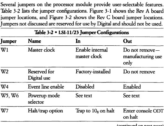
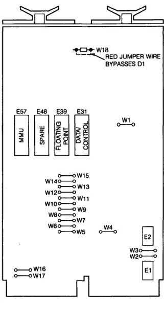
• Configuration
Several jumpers on the processor module provide user-sdectable features. Table 3-2 lists the jumper configurations. Figure 3-1 shows the Rev A board jumper locations, and Figure 3-2 shows the Rev C board jumper locations. Jumpers not discussed are reserved for use by Digital and should not be used.
Jumper
WI W2 W4 W5,W6 W7Table
3·2 • LSI-1l/23Jumper Configurations
Name
In
Out
Master clock
Reserved for Digital use Event line enable Ibwerup mode sdector Halt/trap option
Enable internal Do not remove-master clock manufacturing use
only
Factory-installed Do not remove
Disabled Enabled
See text See text
'frap to 108 on halt Enter console ODT on halt
[image:52.380.50.328.313.527.2]3-3
Table
3-2 • LSI-H/23Jumper
Configurations (ConL)Jumper
Name
In
Out
W8 Conventional Fbwerup to boot- Fbwerup to boot-bootstrap start strap address strap address address, enable if 1730008 selected by
powerup mode 2 is jumpers W9-W15
selected
W9-W15 User-selectable See text See text bootstrap starting
address for power-up mode 2
W16 Reserved for Must be installed Do not remove Digital use
W17 Reserved for Must be installed Do not remove Digital use
[image:53.386.48.325.45.251.2]3-4 • KDFll-AA ISJ-11123 Microcomputer
E57 E48 E39 0--<>
W18
01
~W19
E31 o----Q W17
00
(!) ...J21- ~~
~~
«I-I~
0 0 o~...JQ.
u. u
o----QW15 W140--<>
o----QW13 W120--<>
o--<>W11 W10o----Q
o--<>W9 W80--<>
o--<>W7 W60--<> W4
O--<>W5 0--<>
IW1
W2
C>----<l W3
[image:54.379.95.274.57.349.2]H
8
+D+W18
'-- ... REO JUMPER WIRE
E57 E48 E39 E31
~~
(!) ..JZt- ~~ ~~ <t-OO O~
..JCL.
U. U
o--oW15 W140--0
o--oW13 W120--0
O--OW11 W100--0
O--OW9 W80--0
o--oW7
BYPASSES 01
W1 0 - - 0
W60--0 W4 O--OW5 0--0
[image:55.379.104.265.62.367.2]o--oW16 o--oW17
Figure 3-2 • LSI-11123 Jumper Locations (Rev. C)
Master Oock - WI
3-5
The intemal13.8 MHz oscillator is disconnected from the clock. circuitry
if
WI is removed.This
jumper is used by Digital manufacturing and is not to be removed by the user.Event Line - W4
The bus signal BEVNT causes the event line flip-flop to be set. When the processor enters the service state, the request will be honored
if
the PS <07:05> is5 or less. (BEVNT is a level 6 interrupt.)This
causes the microcode to clear the request flip-flop and trap to the line clock vector (location 1008), H3-6 • KDFll-AA LSI-11123 Microcomputer
Powerup Mode Selection - W5 and W6
Four powerup modes are available for user selection. Selection is made by removal or insertion of jumpers W5 and W6 as shown in the following table.
Mode Name W6 W5
°
PC@24,PS@26 R R.1
Console aDT R I2 Bootstrap I R
3 Extended Microcode I I
I = jumper installed; R = jumper removed.
Only the powerup mode is affected - not the powerdown sequence. The fol-lowing subsections describe the sequence of events after executing common powerup, when selecting each of the four modes. The state of bus signal BHALT is significant in powerup mode operation. '!able 3 -3 lists powerup mode console printout.
Table 3-3 • LSI·H/23 Console Po"'erup Printout (or Display)
Mode BHALT Unasserted BHALT Asserted
o
2
3
Processor
will
execute program using contents of location 24 as the PC value.Terminal
will
print out a ran-dom 6-digit number-the con-tents of the program counter. Processorwill
execute program at location 1730008.*
No printout at terminal.
t
Terminal
will
print out contents of memory location 24.Terminal will print out a ran-dom 6-digit number-the con-tents of the program counter. Terminal
will
print out 173000.*No printout at terminal.+ * Normal mode for use with the MXVll options.IT jumpers W15 through W9 are used,
that address will be printed.
t
IT mode 3 is selected and user microcode is not implemented, the processor will trap to memory location 10 and start program execution using the contents of location 10 as the PC value and the contents of location 12 as the PS value.:j: The terminal printout will consist of six octal digits as specified in the table, followed by a carriage return, line feed, and "@" prompt character in all cases.
• POWERUP MODE
°
(PC @24, PS @26)3-7
• POWERUP MODE 1 (CONSOLE ODT)
This
mode causes the processor to enter console ODT mode immediately after powerup, regardless of the state of any service signals.This
mode is useful in a program development or hardware debug environment, giving the user imme-diate control over the system after powerup.• POWERUP MODE 2 (USER BOOTSTRAP STARTING ADDRESS
SHOWN BY
WB-W15)This
mode causes the processor to generate a bootstrap starting address inter-nally by looking at jumpers WBthrough
W15.This
address is loaded into the PC. The processor sets the PS to 3·10s (PS <07:05> = 7s) to inhibit interrupts before the processor is ready for them. IT BHALT is asserted, the processor enters console ODT mode. IT not, the processor begins execution by fetching an instruction from the location pointed to by the PC.This
mode isuseful
fortum-key
applications where the system automatically begins operation without oper-ator inteJ.Vention.• POWERUP MODE 3 (USER MICROCODE- FOR FUTURE USE)
This
mode causes the microcode to jump to optional control chip 37 s, location 76s, and begin microcode execution.This
mode is reselVed for future Digital use and is not recommended for customer use. IT it is erroneously selected, the processorwill
treat it as a reserved instruction trap to location lOs.HaltI1iap Option - W7
IT the processor is in kernel mode and decodes a HALT instruction, BPOK is tested. IT BPOK is negated, the processor
will
continue to test for BPOK. The processorwill
perform a normal powerup sequenceif
BPOK becomes asserted sometime later. ITBPOK is asserted after the HALT instruction decode, the halt! trap jumper (W7) is tested. IT the jumper is removed, the processor enters console ODT mode. IT the jumper is installed, a trap to location lOswill
occur.Note
In
user mode, a HALT instruction execution always results in a trap to location lOs.3-8 • KDF ll-AA LSI-11123 Microcomputer
Starting Address
1730008 -W8
When powerup mode 2 is selected, the processor examines jumper W8 to detennine the starting address for program execution. If W8 and a compatible bootstrap module are installed in the system, the microcode
will
begin execu-tion at 1730008 (the convenexecu-tional starting address for Digital systems). IfW8 is removed, a trap to 48 (nonexistent address)will
occur. If W8 is removed, the processor looks 3t jumpers W9 through W15 for the starting address.Selectable Starting Address - W9through W15
If the user wishes to start execution from an address other than 1730008,
jumpers W9 through W15 can be used to specify the high byte < 15 :09> of the starting address. Jumpers W15 through W9 correspond to address bits < 15 :09>, respectively. Bits <08:00> of the starting address are set to 0 by the processor. Jumpers are installed for logic I, removed for logic
o.
The starting address can reside on any 256-word boundary in the lower 32 Kbytes of mem-ory address space.• Memory Modules
Several memory modules are available for use in LSI-I 1/23 systems. However, modules such as MSVII memory modules that p.erfonn memory refresh locally are required, because the LSI-11/23 does not perfonn memory refresh itself. Other memories
will
workif
provision is made for refresh with some other bus option. However, this will degrade system performance and is not recommended.• Peripheral Options
DMA peripherals should be installed with the faster throughput devices physi-cally closest to the processor and slower ones farther away. The user must ensure that faster devices have adequate access to the bus; otherwise, data drop errors may occur.
3-9
• Floating-Point Options
Two floating-point options are available, the KEFll-AA and the FPFll. These are described below.
KEFll-AA Floating Point Option
The KEFll-AA is a microcoded FPll instruction set that resides in two chips on one 40-pin package that mounts on the CPU board. This option provides the same features as the FPFll floating-point processor described below, but oper-ates at a slower speed.
FPFll Floating-Point Processor Option
The FPFll floating-point processor is a hardware option designed to operate with the LSI-11/23 or the LSI -11123-PLUS central processor units to execute all 46 arithmetic operations of the FPll floating-point instruction set. The FPFll, contained in one quad-height module, executes instuctions six times faster than the KEFll-AA. The KEFll-AA and the FPFll options are mutually exclusive. For a complete list of the 46 floating-point instructions implemented by the floating-point processor, refer to the
PDP-ll Architecture Handbook.
Specifications Identification Size
M8188 Quad
Ibwer Requirements
+
5 Vdc, 5.5 A (typical)Bus Loads
Related Documentation Document nde
None
FPFll Floating-Point Processor Technical Manual
FPFll Field Maintenance Print SetConfiguration
7.5 A (maximum)
Order Number EK-FPFll-TM MP-01285-00
3-10 • KDFll-AA LSI-lll23 Microcomputer
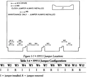
Before installing the FPF 11, run system diagnostics to verify that the system receiving the option is working properly. Then, to ensure proper bus grant con-tinuity, configure the jumper:> as indicated in Table 3-4. Refer to Figure 3-5 for the locations of the jumpers on the FPF 11.
ROW 1 ROW 2 ROW 3 ROW 4
I I
SLOTA I SLOT B SLOTC I SLOT 0
CPU
FPF11 M8188
OPTION 3 OPTION 4 OPTION 6 OPTION 5 VIEW IS FROM MODULE SIDE OF CONNECTORS
Figure
3-3 • FPFIIModule in
LSI-11123System
~W10SPARE ~W9
CLOCK JUMPER ALWAYS INSTALLED
~W6
c
MAINTENANCE ONLY - JUMPER ALWAYS INSTALLED
W12
~
W11
~ we
~
W7
~ ~~ W5 W4 ~ W3
J1
W2
~
1
W1
[image:61.379.43.323.68.320.2]~
Figure 3-5 • FPFll Jumper Locations
Table 34 • FPFll Jumper Con6gurations
3-11
WI W2 W3 W4 W5 W6 W7 W8 W9 WIO Wll W12
R I I I R R I I
R
RI
=
jumper installed; R=
jumper removed• Cabinet Kits
The following cabinet kits are available for use with the various models of the LSI
-11/23
microcomputer:CK-KDFlB-KA For use with the BA23 enclosure (includes a selectable baud switch)
CK-KDFlB-KB
CK-KDFlB-KC
CK-KDF2B-KB
For use with the BAll-M enclosure (includes a selectable baud switch)
For use with the H349 distJ.jbution panel (includes a selectable baud switch)
Chapter 4 • KDFII-B LSI-11123-PLUS Microcomputer
The LSI-1l/23-PLUS microcomputer (KDFll-B) contains a BDVll-compatible diagnostic and bootstrap ROM, a linetime
clock
(LTC), two asynchronous serial lines, a memory management unit (the KTFll-AA), and three sockets for the optional Commercial InstructionSet
(KEFll-BB) and/or floating-point instruc-tion set opinstruc-tions (the KEF 1 l-AA or FPFll). It can address up to four megabytes of main memory.There are three variations of the KDFll-B. Each variation contains a different diagnosticlbootstrap ROM, supporting various bootable devices, as listed in Table 4-1.
Table 4·1 • KDFll·B Variations
Supported
Devi~es
KDFll·BA
KDFll·BE
KDFll·BF
RXOl yes yes yes
RX02 yes yes yes
TU58 yes yes yes
RL01/2 yes yes yes
MRVll-C yes no no
RX50 no yes yes
RD51 no yes yes
RD52 no no yes
TSV05 no no yes
TK25 no no yes
RC25 no no yes
DEQNA no no yes
DLVEI yes no no
DLVll-F yes no no
4-2 •
KDFll-B
ISI-11123-PLUS Microcomputer• Specifications
Identification
Size
Power Requirements
Bus Loads
ac dcPerfonnance
Instruction Timing Interrupt LatencyInterrupt Service TIme
DMALatency
M8189 Quad
+
5V
± 5%, 6.4A
maximum (4.5A
typical)+
12 V ±5%, 0.7 A maximum (0.3 A typical)2 1
Based on 75 ns intelVals 5.7 microseconds (typical) 12.6 microseconds (maximum), exceptEIS
54.225 microseconds (maximum), including EIS
8.625 microseconds (memory management off) 9.750 microseconds (memory management on) 1.35 microseconds (maximum)
Note
Interrupt and DMA latencies assume a KDFI1-B
with
memory management enabled and using MSVII-P Memory.Nonstandard Environmental Specifications
Operating temperature 5°e to 500e (41°F to 122°F)
Operating altitude Up to 2.44
Ion
(8,000 ft)• Related Documentation
Document TIde
KDFll-B CPU Module User's Guide
PDP-11123B Mounting Box Technical Manual
PDP-11123B Mounting Box User's Guide
KDFI1-BA Field Maintenance Print Set11/23-B Field Maintenance Print Set
I1T23-B Field Maintenance Print Set
4-3
• Configuration
Jumper and Switch Configuration
The LSI-1l/23-PLUS contains two dual inline pack (DIP) switchpacks (E102 and E114) and several jumpers that allow the user to select the module features desired. The location of the switchpacks and jumpers is shown in Figure 4-1. The boot/diagnostic switchpack (E102) consists of eight switches that let the user select boot and diagnostic programs. The second switchpack (E1l4) selects the baud rate for the console SLU and the second SLU. The module con-tains both wirewrap jumper pins and soldered-in jumpers. The jumpers are divided into the following functional groups:
• Test jumpers • CPU option jumpers