1971
mamooma
CONTROL HANDBOOK
Copyright
©
1968, 1969, 1970 by Digital Equipment CorporationDigital Equipment Corporation makes no representa-tion that the interconnecrepresenta-tion of its modular circuits in the manner described herein will not infringe on existing or future patent rights. Nor do the descrip-tions contained herein imply the granting of licenses to make, use, or sell equipment constructed in ac-cordance therewith.
INTRODUCTION TO SOLID STATE
K SERIES CONTROL LOGIC MODULES
A SERIES LOGIC MODULES
UNIVERSAL HARDWARE AND ACCESSORIES
K SERIES APPlIC"TIONS
CONTROL PRODUCTS
NUMERICAL CONTROL PRODUCTS
PDP-14 PROGRAMMABLE CONTROLLER
CONTROL SYSTEMS
TRAINING AND DESIGN AIDS
ACKNOWLEDGEMENTS
The production of a publication of this size and complexity can be achieved only through the efforts and cooperation of dozens of people. These include engineers, writers, artists, and production personnel. While it is impossible to cite all, a few individuals deserve special mention. Among these are: John Bloem of the Control Products Group engineering staff who prepared and assembled most of the technical material for this Handbook; Elliott Hendrick· son and his staff for their art direction and production assistance; and Joseph Codispoti for his editorial assistance. The cover of this Control Hand-book was conceived and executed for Digital by Chris Murphy of Boston.
FOREWORD
The DIGITAL Control Handbook is presented by Digital Equipment Corpora-tion as a practical guide to solid state control logic. It is written for those who specify, design, manufacture or use electronic or mechanical logic for control of equipment ranging from basic stand alone machines, to complex transfer and processing equipment, to sensitive laboratory instrumentation. This fourth edition contains information on the latest developments in Digi-tal's products for control and documentation on current techniques of their application.
For readers investigating solid state control logiC for the first time, this book is especially appropriate as it contains a meaningful orientation to solid state, showing its relationship to older forms of electromechanical control. Part of this orientation is comprised of a straightforward presentation on how to convert from relay to solid state logic. Several practical examples are given on how the conversion is executed.
Of particular interest to machine tool builders and users, is the introductory documentation contained in this handbook on the new PDP-S based sys~
tem for direct numerical control. This edition also contains data on our sub-stantially expanded line of analog logic modules, designed for a variety of industrial and other applications which require analog data handling with digital techniques. A brief description of the Corporation and its other pro-ducts is also presented.
TABLE OF CONTENTS
Thumb Index
Foreword
INTRODUCTION TO SOLID STATE.
K SERIES CONTROL LOGIC MODU~ES .
Logic Symbology
Logic Module Data Sheets:
Gating Modules, KOXX and KIXX . Flip-Flops and Memories, K2XX .. Timers, K3XX " ... . Manual Control Modules, K4XX .
Interface Module Data Sheets: Inputs, K5XX
Outputs, K6XX .
K Series Hardware and Accessories:
Accessories Containing Electronics, K7XX . Mounting Hardware, K9XX ..
A SERIES ANALOG MODULES
UNIVERSAL HARDWARE and ACCESSORIES
K SERIES APPLICATIONS
Construction Recommendations Relay Logic to K Series Conversion ." Sequencers, Introduction .... . Timer Sequencers. . ... ~ .. . Counter Sequencers .. Shifter Sequencers ... Polyflop Sequencers ..
Using K303 Timers for Frequency Setpoint .. Estimating K303 Time Jitter ....
Combining K with M Series Modules. Combining K with A Series Modules . Combining K with R Series Modules Pulse Generator From NAND Gates K531 Quadrature Decoder. Sensor Converters ... .
DC Drivers.
Using K210s for Long Odd-Modulus Courtters .
TABLE OF CONTENTS (Con't)
K SERIES APPLICATIONS (con't.)
Parallel Counters Annunciators
~ultiplexing Thumbwheel Registers with K581 Fixed Memory Using K281 ,
Pulse Rate Multiplier, Pulse Rate Squarer, Digital Integrator Serial Adder
Stepping Motors, Introduction Basic Two Way Shift Register SLO-SYN Bifilar Motor Drive Responsyn Motor Drive Fujitus Motor Drive
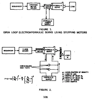
ElectrohydrauJic Servo Motor ,
Voltage to Frequency Converter Using A207 Current to Frequency Converter Using K303 Using K604, K614 with 240 V
CONTROL PRODUCTS
Numerical Control Products,
Quickpoint-8 NC Tape Preparation System Direct Numerical Control
PDP-14 Programmable Controller
Control Systems
Training and Design Aids: K Series Logic Lab Computer Lab
ABOUT DIGITAL EQUIPMENT CORPORATION
Warranty Statement and Discount Schedule
Price List and Numerical Index
Index ,310 311 313 315 316 317 318 320 321 324 324 325 326 328 329 330 331 334 336 338 , 352
Introduction
toS61id State
Control system complexity and demands on reliability are rising with ever-increasing automation. More and more, control system designers are looking to solid state electronics for new answers to the old problems of reliability, complexity, and economy. Some of the answers are provided by solid-state digital logic deSigned for the industrial environment, and solid state analog-digital conversion to link analog sensors and actuators to analog-digital control.
Why Solid State?
The time-honored way to do control logic is with the deceptively simple-looking relay. The metal-to-metal contact area sees physical and chemical actions of remarkable complexity. Even the mechanical-magnetic interactions are involved enough to cause problems now and then. Still, relays sometimes respond beautifully to simple maintenance. If the contacts stick, force them apart; if they are dirty, clean them.
Railway signaling relays, operating perhaps a hundred times a day,' accumu-late 25 years and a million operations without failure. And modern sealed-contact relays can do 10 billion operations under the right conditions without wearing out. So why abandon well-proven, reliable components? Don't, unless it is necessary! But it is becoming necessary in
a
growing number of applications.Reliability
As profit margins grow tighter, and maximum process efficiency becomes a neCessity rather than an ideal, control system reliability assumes greater importance. Faulty operation and machine downtime can swiftly and
I
trously cut into the profit picture. With a highly complex control system, check-out can easily become a very costly and time consuming operation. Many factors affect the reliability of a control system. A major consideration is the speed at which. the logic control elements must operate. At 1 KHz, near the maximum rate for dry reed delays, 100 million operations accumulate in about 30 hours. Longer·lived mercury·wetted contacts, operating 100 times per second, accumulate 10 billion operations in about four years. Even if a four year component life is enough, there are applications where 100 opera-tions per second are not. Solid state logic, with nothing to wear out, stick, or corrode, can operate almost indefinitely at 100,000 operations per second.
Complexity is another factor. Demands for more automation, more efficiency, more safety, more accuracy all result in increased control system complexity. As a result, the sheer numbers of logical decisions demand component reliability far greater than that acceptable in a small system. Solid state logic provides the degree of reliability needed in a large system, at reasonable cost.
Size
Even the tiniest-contact reed relay coil is enormous alongside a transistor, or a complete integrated circuit, and most small control systems are not built with reed relays: to get the advantage of ruggedness or standardization, usually all the relays used are built to 300 volt or even 600 volt specifications whether they drive external loads or just relay coils. But a single small printed circuit board can easily accommodate a half dozen or more relay equivalents in logic capability, in a small fraction of the space of one 300 volt relay.
Computer Tie-In
There are several levels of computer involvement possible, extending from incorporation of a computer as a part of an individual control system to the use of a central computer to monitor the performance of many independent control systems. Regardless of the level at which the computer interacts, its presence demands an interface between solid-state Circuitry and the con-trolled machine or process. If such an interface is forced into existence by the present or projected future use of a computer, why not put solid state control logic behind it and gain the benefits of solid state speed, compact· ness, and reliability throughout the entire system?
Also, solid-state logic can communicate with existing analog sensors and actuators through solid-state analog-to-digital (AI D) and digital-to-analog
(01 A) converters.
All of these factors tend to make solid state control systems increasingly attractive, particularly as their costs come down.
Who Should Be Designing For Solid State Controls?
Broadly speaking, the decision between conventional relay controls and the new solid state controls, like most engineering deCisions, hinges on compara-tive overall costs. Where three or four or a half dozen relays can do the whole job, the cost of a solid-state interface will seldom be justified unless high speeds are required .. Very large or computer-oriented systems leave little justification for the use of relays.
Considerations
Reliability
Cost
Complexity
FactO,rs Suggesting Relays
Control system failure causes no panic. Temporary manual control acceptable. Simple system, easy to trouble shoot.
! Factors Suggesting I Solid State
Downtime cuts quickly into process profitability. Quick check-out of entire system in case of trouble desirable, instead of on-the-spot check-ing. Lives and property might be endangered by failure. low cost relays acceptable. High quality relays used for Maintenance costs need not comparison. Costs of failure be considered-. Personnel high. Installation space cost-training costs important. Sys- Iy. Cost of future modifica-tern failures will not cause tions must be considered. significant secondary costs. Maintenance costs over life
could be important. Small systems" perhaps a Complicated systems, which half dozen relays or fewer. would require fifteen or more
relays to implement. Sophistication Traditional performance still New levels of performance
Familiarity
Growth
Size
Speed
\ acceptable. are needed, calling for
in-I
creased control system com-l pcom-lexity to remain competitive. Controls must be servicedby electricians who can not be retrained.
No foreseeable use of com-puters. little likelihood of important modifications.
Plenty of space available.
Control system delays of tens of milliseconds accept-able. Operating rate is low, relay wearout no problem.
Environments already in-clude other solid-state com-ponents or they will soon be added. Also, mUlti-system installations where a few controls technicians will cover a lot of equipment. Added perfo'rmance or safe-ty features may be wanted later without tearing the system down. Computer tie-in might become' desirable or is planned already. Relay equipment might quire separate balconies, re-strict maintenance of ma-chinery, or block aisles. Features added later must fit original enclosu~e.
Why Digital?
Relays, solenoids, switches, fuses, locks, counters, annunciators, panel lights and panic buttons all have one thing in common: they are digital. All these devices (when working properly) are up, down, on, off, in, out; but never in-between. Strictly speaking, of course, you cannot get from on to off without passing through in-between. But digital devices pass through in-between at maximum speed, and without waiting around for doubt to creep in.
Non-digital devices like panel meters, potentiometers, and slide rules work in the "in-between" area, producing outputs that are proportiona~ to the input. The angular position of a panel meter pointer is the analog of the magnitude of the electrical input. A potentiometer's voltage output is the analog of mechanical shaft position. In a slide rule, position is the analog of magnitude.
In a slide rule, accuracy is limited by the thickness of the calibrating marks and the difficulty of estimating values between them. Each space is an area of· uncertainty. The same kind of uncertainty exists in every proportional electrical system, in the form of noise. In all but the most expensive analog equipment, the amount of noise, like Slide rule error, limits accuracy to two or three significant figures.
Noise taken in this broad sense affects every proportional device. Noise is a major reason for the dominance of digital computers over analog computers where complex calculations are required. Small amounts of noise con-tributed by each analog input or computing element add up to degrade the accuracy of the answer. In digital circuits, the noise can be disregarded as long as it is below an "off" or "on" threshold level.
Analog controllers and servo systems, chart recorders, panel meters, and small analog computers are often simpler and cheaper than their digital equivalents, and should be used wherever they can do the job. But since so many commonly used control devices (from relays to panic buttons) are digital anyway, all-digital control is convenient. For complex control situa-tions, digital methods can deliver accuracy and perform types of control beyond the ability of an analog system at any cost. And using solid state digital control, analog and digital devices can work together through
AI
0 andOf
A conversion. Better still, noise-free direct digital sensors and actuators can be used in the design of new process equipment.Noise Immune Control Modules
Because ,of their high sensitivity and speed, solid state components can respond to noise that relays would safely ignore. To use solid state logic with freedom from noise problems in the neighborhood of arcing contacts, brushes, welders, etc. requires special design considerations.
'In the design of solid state logic for industrial use, this basic threshold feature of digital circuits can be exploited. By adding external capacitance, the speed, and thus the sensitivity, of the circuit can be lowered.
Noise
Suppose that on the basis of the above, you find you should be using solid-state digital logic. But will the system "drop bits," or otherwise go haywire in your environment? How well can noise trouble be anticipated, and what measures should be taken? How can you compare the noise immunity of competing manufacturers' circuits? These questions need some kind of answer before you can feel confidence in taking th~ step.
A logical starting point is the noise itself. What is its amplitude? Its fre-quency distribution? How does it vary with time? With temperature? How many picofarads of coupling capacitance between the noise sources and the logic wiring? 'How many nanohenries of shared inductance in the logic and
noise ground return paths?
Right away you suspect these questions are going to be difficult to answer. You may be able to say that typical noise source voltages are "measured in kilovoltS" and are "strongest in the Megahertz frequencies." But going beyond such hazy estimates will require detailed knowledge of the physical conditions that interact to produce electrical noise .. You'll need to know the materials used in all metal-to-metal contacts, and the condition of the contact surfaces. You'll need the inductance and capacitance of the wires connecting them, the inductance and capacitance of the loads they drive, and the gases in the atmosphere surrounding the contacts. Even the exact routing of the wires will have to be examined.
I
K SERIES
CONTROL MODULES
Computer-oriented logic, by its very nature, is high speed (1 MHz and above), and provides noise immunity far below that required in a process control environment. The upper frequency range of the K Series modules is 100 KHz, with provision for reduction tq 5 KHz for maximum noise immunity. These modules incorporate all silicon diodes, transistors, and integrated circuits, deliberately slowed through the use of descrete components.
Either English (non-inverting) logic or NANDI NOR logic is compatible with K Series. The hardware for this series is specifically designed for standard NEMA enclosures. FLIP CHIP mounting hardware can likewise be used for
rack-mounting, inasmuch as K Series ":,odules fit standard DEC sockets. Proven FLIP CHIP connectors, used for years in applications from steel mills to lathe controls, provide modularity. Even the connection between terminal strips and electronics can be plugged for installing the logic after field wiring is complete, and removing it quickly for modifications or addi-tions.
Checkout and trouble shooting is easy with K Series logic. Wherever possible, every system input and output has an indicator light at its screw terminal. A special test probe provides its own local illumination and built-in indication of transients. as well as steady states. Every point in the system is a test point, and consistent pin assignments reduce the need to consult prints. Construction materials and methods are the same as for other high-production FLIP CHIP ",odules, including a computer-controlled operating test of each complete module. K Series modules further offer the size reduction, reliability, flexibility, and low cost of solid state logic, with an added bonus of easy interconoection. FLIP CHIP industrial modules are ideal for interfacing high speed M Series or computer-systems to machinery and processes. Sensing and output circuits can operate at 120 vac for full electromechanical capability. Inputs from contact devices see a 1110derate reactive load to assure normal cont~ct life. Solid state ac switches are fully protected against false triggering. Voltages from the external environment are excluded from the wire·wrap connections within the logic.
K SERIES SPECIFICATIONS
SUMMARY
Frequency range: ~ to 100 KHz. Control points on the modules allow reduc-tion to 5 KHz for maximum noise immunity for critical funcreduc-tions.
Signal levels: Ov and +5v, regardless of fanout used.
Fan-out: 15 rna available from all outputs; typical inputs 1-4 mao
Waveforms: Trapezoidjil. No fast transients to cause cross talk. External capacitive loading affects speed only; no risetime dependence.
Noise immunity: false "1":30 rna at 1.6v for 1.5 p.sec typical. false "0":3 rna at 3v for 1.5 p'sec typical. Time thresholds can be increased by a factor of 20 for critical points by wiring the slowdown control pins.
Simple power requirements: Single voltage supply, +5v ± 10%. Dissipation typically 200 mw per counting or shifting flip-flop, 30 mw per control flip-flop, 10 mw per two-stage diode gate.
Control system voltage: 120 VAC, 50 or 60 hertz.
Mounting provisions: Standard NEMA industrial enclosures. May also be used in 19" electronics cabinets.
GENERAL SPECIFICATIONS
Construction Features
K-Series modules include the quality features of older lines of FLIP CHIP modules: flame-resistant epoxy-glass laminates, all-silicon semiconductors, gold plated fingers and solid gold connector contacts. Thorough testing of each module is by computer operated automatic tester for most modules, or _by specialized equipment for those which are not amenable to automatic test. A test specification sheet or data sheet is packaged with each module, includ-ing a circuit schematic for that type. Monolithic or hybrid integrated circuits are included wherever they can improve the performance-cost ratio. Versatile mounting hardware imposes as few physical constraints as practicable. Outline drawings below show nominal module dimensions.
STANDARD MODULE SIZES
SINGLE -WIDTH FLIP CHIP MODULE
CONDUCTIVE COMPONENT LIMIT 11/32 0.056
!
NONCONDUCTIVE COMPONENTS 3/8 mox.~--- ---~
~l-=;~===~==D=-P=L=~=E=D=CON==T~==T=S~~====~~3lJL~
1/16 MAXIMUM HEIGHT
OF SOLDERED ETCHED WIRING SURF~E
COMPONENT LEADS
DOUBLE-WIDTH FLIP CHIP MODULE
CONDUCTIVE COMPONENT LIMIT 13/16 O.OM
1
NONCONDUCTIVE COMPONENTS 27132 max.~-
-r----i
t
GOLD-PLATED CONTACTSDOU8LE - HEIGHT FLIP CHIP MODULE
':~ITEg
r-=~
.. ,
T
FI==F
g
AH2
1
'40f
.140~
~
.370 t AU
*
~
AV53116
t
T
2.240L
IA INI ec 8D If: IIf 8M 8J 8K 8l 8M lIN 8P 8111 IS BT 8U BV3/32
=1-1----.
812o
o
5'/'6
---...-(.1
1 ..
· : - - - -5 1/2
---404
Logic Signals
There are no ultra-fast transients at any K Series output. Logic signal -1"
and "0" levels are essentially independent of fanout. Rise and fall transitions have controlled slopes which are not strongly influenced by normal changes in fanout, lead length, temperature, or repetition rate. The fastest K Series trapezoidal logic signal can be fully analyzed with a 500KC oscilloscope. Logic "I" or "true" is +5 volts and lokic "0" or "false" is zero volts except where redefined by logic designer. Counters and shift "registers advance at the "I" to "0" transition and are cleared by a "0" level Any unused input may be left open.
M Series Compatibility
Loading
Input Loading (Fanin)-Each K Series input requires a certain amount of drive to operate, thus imposing a load on the output driving it: The amount of load imposed by an input is defined in terms of the amount of current required to pull that input to ground. Logic gate inputs consume 1 milli-ampere per input. Other loadings range from 1 to 4 millimilli-amperes as indicated by the loading numbers enclosed in squares on each specification diagram.
INPUT LOADING:
1 MA PER INPUT
FANIN AND FANOUT
DRIVING CAPABILITY
EACH OUTPUT DRIYEN IN A "WIRED AND" IS
A 3 MA LOAD
Output Loading (Fanout)-Each K Series output is capable of sinking a certain maximum amount of current to ground in the low state. The standard K Series output can sink 15 milliamperes to ground and can therefore handle a maximum of 15 inputs, each requiring 1 milliampere of drive.
If K Series outputs are paralleled to obtain the wired AND logic function, each gate output is effectively driving the other and therefore, each output must be considered as a load on the others. To pull a typical output to ground requires 3 milliamperes of drive. When two or more K Series outputs are tied together, they produce a 3 milliampere load on each other. If, for example, the outputs of th.ree K123 gates are connected, the combined fanout is' reduced by 6 milliamperes, leaving 9 milliamperes of drive capa-bility. A maximum limit of five outputs can be tied together reducing the fanout capability to three milliamperes.
Operating Temperature .
K Series modules are designed for operation in free-air ambient temperatures between -20°C and +65°C (O°F to 150°F) except. the following types which are restFicted to O°C (32°F) minimum: K201. K202. K210. K21l, K220, K230, K596.
Speed
Many applications for K Series modules involve operation at rates lower than relay speeds. Even at speeds many times faster than relay capabilities, timing need not be considered unless the logic includes a "loop". fA flip-flop con-structed of logic gates is such a loop, in which the output at a given point feeds back to influence itself, thus demanping input durations longer than total loop delay. Proper operation of such loops should be verified by calcu· lation using the specifications below. For a complex loop an experiment should be made if possible to look for flaws in the calculations.
ex-amined just as carefully in slow logic as in fast logic. If K Series speed ap· pears marginal or insufficient for the job at hand, use M Series high speed logic modules.
OK SERIES TIMING
Timing Characteristics for K113, K123, K124, Time (,usec)
K202, K210, K211, K220, K230 Min. Typ. Max.
Logic Gate Propagation Delay, Time Delay for 0.5 2.0 3.0 output to rise to 2.5v after input is sensed.
Output D only, when connected to pin B 7.5 40 ISO
Logic Gate Propagation Delay. Time Delay for 0.3 1.0 6.0 output to fall to 2.5v after input is sensed.
Output D only, when connected to pin B 4.5 20 180 Countl Shift input Propagation Delay, Output 2.0 5.0 9.0 Rise.
As above, but pin B grounded to pin C 10 30 100 Count/Shift Input Propagation Delay, Output 1.0 4.0 9.0 Fall
As above, but pin B grounded to pin C 10 30 100 Rise time, all unslowed outputs, Kl13, K123, 2.0 7.0 12.0 K124. (Ov to +5v)
Pin 0 output only, when connected to pin B 30 140 240 Falltime, all unslowed outputs, Kl13, K123, .5 1.5 4.0 K124 (+5v to Ov)
Pin D outputs only, when connected to pin B 7.5 30 120 Minimum time between successive input tran- 4
sitions on any module which has one or more
Countl
Shift inputs.As above, but pin B grounded to pin C 10
ExceptIons:
Input transitions at pins J and K may follow other input transitions with delays down to zero; For characteristics not listed above, see timing information on individual data pages.
NOTE: Count/Shift inputs are included in types K202, K210, K21l, K220, and K230
Noise Immunity
thou-sands of vorts. Consequently, voltage thresholds alone cannot provide ade-_ quate noise rejection. The noise appears to come from a current source, so
that logic circuit current thresholds are' also an important measure of noise . immunity.
Another means of controlling noise is by timing thresholds. Capactive--coupled interference is strongest at high frequencies. Logic circuits whicti respond slowly can reject high frequency interference peaks that exceed the current and voltage thresholds.
Noise immunity in K Series modules is provided by a balanced combination of voltage, current, and timing thresholds. Techniques for increasing these noise reje~tion thresholds will be discussed in the remainder of this article.
, Typical K Series noise thresholds are as follows:
1. To be falsely interpreted as a high (+5) level, a low (zero volts) K Series logic level must be raised 1.6 volts and held there for 1.5 microseconds. To do this would require 30 milliamperes to be supplied somehow from the noise source to the K Series output in question for this period of time.
2. To be falsely interpreted as low level. a high (+5) K Series logic level would have to be reduced 3.4 volts and held there for 1.5 micro-seconds, to do this would require 3 milliamperes to be supplied some-how from the noise source to the K Series output in question for this period of time.
Voltage threshold: The typical K Series circuit is a single voltage threshold device. This means that the circuit will turn on (low to high) at the same voltage threshold as it will turn off (high to low).
INPUT
!.U~!!!}.y
________
~~~~F
I ,
, I
I
OUTPUT - - _ ....
1
Some K Series modules, however, have a built-in feedback network which increases the voltage threshold necessary to switch from a low to a high output and decrease the voltage threshold needed to switch from a high to a low output. This results in a voltage gap between the turn on level and the turn off level, which is known as the hysteresis of the circuit.
TURN ON 5V' HYSTERESIS
::J
DJj¢.11JZ7.DnlF.£ZF¥.Rtfi!~URN
OFF
I N P U T : ;
-I I
OUTPUT _ _ _ ...
1
5V
Those K Series modules which contain hysteresis have voltage gaps from .5 to 1 volt in width, resulting in a higher voltage threshold necessary to turn the circuit on. As an example: suppose a circuit turns on at 2.4 volts and turns off at 1.4 volts, then it would require a noise spike 2.4 volts high and 1.5 microseconds wide to trigger a false high level. To be falsely interpreted
as
a low level, a high level (+5) would now have to drop 3.6 volts for 1.5 microseconds.Current thresholds: Current thresholds change with each variation in a circuit's voltage threshold. If a circuit has hysteresis, the noise source will need to supply the K Series output with even more current in order to cause a low level to be falsely interpreted as a high level, or a high level to be falsely interpreted as a low level. As an example: suppose a circuit has 1 volt hystersis; if the turn on voltage threshold is 2.4 volts, then the noise source will need to supply 60 ma to the K Series output for 1.5 micro-seconds to obtain a falsely interpreted high output. The current threshold necessary to falsely interpret a low (0 v) level will increase to 3.2 mao
Timing thresholds: All critical K Series outputs contain a slowdown, which prevents operation at frequencies above 100KHz. Many modules also pro-vide pin connections for further slowdown to 5KHz. As discussed apove most noise occurs at high frequencies, therefore the slower the logic circuits the more noise immunity. A typical example of slowdown in K Series:
INPUT - - _ ...
UNSLOWED
~
OUTPUT
---f.
~7p.S~
- - -'5V
----ov
I I
5V
SLOWED I
OUTPUT ----~ I I OV
I--
14010'$~
-.f
3010'5~
With 5KHz slowdown connected, 'a noise spike must now maintain the necessary voltage and current threshold levels for 30 microseconds instead of the typical 1.5 microseconds at 100KHz.
If a particular point in a logic system is exceptionally noisy, a, capacitor can be hung to ground from that point. This method of noise reduction can be used because K Series logic does not care what rise time you feed it.
RESET
SET A
SET B
I
I
I
L-o
I
I
DOTTED LINE SHOWS WIREI
ANDThis precaution prevents noise problems in the system.
Up to this point, only those methods which can be used to' minimize the influence of noise that has already entered a logic system have been discussed. Keeping noise out of a system, however, is far cheaper than electrically rejecting it. In this section, several methods of keeping noise ou.t of a system will be discussed.
1. Segregate logic wiring from field wiring. Never design input converters and output drivers so field wiring goes through the same connectors used to carry logic signals. Arrange to use opposite ends of printed boards for logic and field wiring connections, and never allow the two kinds of wiring to be side-by-side or be bundled together.
2. Never mix, logic ground with field ground. This does not mean that logic ground should float. Heavy currents should not pass through the logic ground system on their way back to a power ·supply. AC and DC isolation techniques used in K Series are as fololws:
PC IsolatiOn-AC ,Input Converters and AC Isolated Switches use transformers to isolate AC voltages from the logic. The inductance of the transformer windings prevents AC noise spikes from penetrat-ing the logic circuit.
'~
C
--+ TO LOGICAC
-VOLTAGE
AC ISOLATION
heavy currents in th~DC ground level will be forced to flow t~rough the ground return wire and not through the logic ground (path of least resistance.) The isolation resistor looks like a very high reo sistance compared to the ground return wire of the load supply.
INTERNAL DC ISOLATION
IN DC DRIVER MODUr LOAD SUPPLY GROUND RETURN
+
LOAD SUPPLY
r-.. -.... -...
.,.---+----I
I ~--~
CHASSIS GROUND
3. Use high·density packaging. Computer type modular construction minimizes lead lengths in the logic, minimizing the capacitive coupling between logic wiring and nearby field wiring. Dense packaging also cuts resistance and inductance'jn the logic grounding system, minimiz-ing interference from any residual noise currents that may flow there.
4. Where logic 'and power circuits must be adjacent, us~ shielding. For example: a group of printed boards carring field circuits can be shielded from general purpose logic modules simply by inserting un-etched copper clad boards in the sockets that separate the two groups. (Logic power must skip these sockets to avoid shorting the'supply.) A single ground connection to the shield board is perfectly adequate, since the noise currents it carries will be limited by the small capaci· tance involved. (W993 electrostatic shields may be used.)
5. Filter the line voltage where it enters the logic power supply, or at' supply output terminals. Supplies for panel lamps should also be filtered, if their wiring approaches logic wiring. Do not use logic power for any other function or carry supply output wires into the field for any reason.
Power Requirements
A simple 5 volt supply operates any K Series system. Tolerance at room temperature: ± 10%. K Series regulators K731 and K732 have a built'in temperature coefficient of approximately minus 1 % for 3°C(5°F) to obtain full logic fanout over' a wide temperature range and to minimize the tem-perature coefficient of K303 timers. Both regulators run from a nominal 12.6 volt center·tapped transformer secondary, with hash removed. See
K SERIES LOGIC SYMBOLS
Symbols used in K Series diagrams are based on standard ICl-1965-158 for industrial controls issued by the National Electrical Manufacturers' Associa-tion ("NEMA"). For those not familiar. with this standard, the basic symbols are defined below, along with equivalent symbols from U.S. Military Standard Mil STD-806B. K Series modules are designed to allow a logical "1" to be. identified with the positive voltage level, and logical "0" with zero volts. The diagrams shown below follow this convention. Notice that except for tfm-ers, the two symbol standards are one-for-one interchangeable. For relay logic symbol conversion, see second Applications Note.
C;ERIES SYMBOL LOGIC FUNCTION MIL SYMBOL
A a A AND a
0 0
o
(FAL!E10 f
o
(I"ALSEI.
,
0o
(I"ALKI, ,
, (TMlEI·U···
A· 8.~
...
I
A.II . (A AND II· A I (A AND I)
AND
~
ANDA·a
I
-A I AORa
0 0
o
(I"ALSE)0
,
I (TMlE),
0 , (TAUE)·D·VI
f f I (TlltU[)'D----c'V.
A., 1..1
• (A Ollt a)
I
8 (A Ollt I)A
OR
~
ORA.a
I
'N-
-[ill]
NOT o f
AV
i
, 0
NOTE: OVERSAR MEANS NEGATION If' A
K SERIES SYMBOL
z Y X W
BINARY COUNTER
'z y X W BCD COUNTER (BINARY-CODED DECIMAL)
OFF DELAY (WITH GATED INPUT)
%
CONVERTER
LOGIC FUNCTION
A
1111111111111111
~
~,
~
Z
L
A
1111111111
~
I0 : L
~
DELAY~ ~
CONVERTS AC, DC, OR RESISTANCE TO LOGIC LEVELS AND
VICE-VERSA
. MIL SYMBOL
Z Y X W
BINARY COUNTE"R
z y X W
.-
--BCD COUNTER ~BINARY-CODED DECIMAL)
OFF DELAY (WITH GATED INPUT)
-1
CONVERTER CONVERTER~
K SERIES lOGIC
K Series is organized by groups according to ,the first number after the K.
KNXX
These groups are as follows:
N==O N==l N==2 N==3
N=4
N==5N=6
N==7 N==9Gate Expanders Gating
Memory (flip-flops, counters, etc.) Timing
External Controls Input Converters Output Converters Power
Hardware
WHAT IT DOES.
A. GATING-KIOO GROUP
K Series gating modules combined with K Series gate expanders provide an extremely versatile method of implementing logic functions. Functions of high complexity can be implemented inexpensively using these gates and expanders.
The basic K Series gates are the Kl13 Inverting gate and the K123 Non-inverting gate.
K113
A
INPUTS
B
The K1l3 performs the NAND function F
=
(A7B)The K123 performs the AND function F
=
(A • 8)K123
Notice that each basic K Series gate shows two inputs with dotted lines. These are the expansion inputs, which allow functions other than NAND or - AND to be implemented.
AN)
The "AND" expansion input is used with the K003 AND Expander, to provide the AND or NAND function for more than 2 inputs. For example, with one K003 AND Expander connected to a K123 Non-inverting gate we create a five input AND gate.
A B
C
o
E
Up to
lob
inputs may be connected to the AND Expansion input.The "OR" expansion input is used with the K026 "AND/OR" expansion gate, or the K028 "AND/OR" expansion gate. Used with the K012, the K123 (or Kl13) becomes a 4 input "OR" (or Nor) gate.
F=A+B+C+O
Up to 9 "OR" inputs can be connected to the_ OR expansion input.
When the OR expansion input is used, and the AND inputs are also used, the output of the AND gate is "ORed" .with the OR expansion input.
A
The K003 can be connected to the OR expansion input as follows:
A
B
c
o
We can now begin to see the power of K Series gating. For instance, the function (A • B • C • 0 • E)
+
(F • G)+
H+
I+
J+
K can be simply implemented with I KI23, 2 K003, I KOI2 as follows:A
B
C
0
OUTPUT
E
F
G
H
I
J
K
Producing functions with K Series logic takes some practice and ingenuity on the part of the logic designer, but once mastered will save money and
time. '
Some of the other functions available in the"KIOO series are Binary_ to Octal Decoder
Equality and Digital Comparators Rate Multiplier
The Binary to Octal Decoder (KI61) takes a 3 bit binary number and pro-duces one out of eight lines high.
The fquality Comparator (K171) tells if two binary numbers are equal. The Digital Comparator (KI74) tells which of two binary numbers is greater.
B.
MEMORY...;...I(2QO GROUP
K Series contains a full line of flip-flops, counters, shift
reciStetS,
and memory accessories.In flops, there are set· reset types (K201, K206) and Data (K202) flip-flops.
The K202 Data flip-flop looks as follows:
CLEAR
OUTPUT OUTPUT
(INVERTED)
The 0 type flip-flop output goes to the state of the D input when the clock input falls from high to low. Notice the built in gates with expansion inputs on the clock and Data inputs. These allow simple input conditioning. K Series has two counter modules. The K210 is a binary or BCD up counter (4 bits). Using expansion gates, it can be connected to count anywhere from 2 to 16.
BINARY/BCD
The K220 is a binary or BCD up/ down counter which can be parallel loaded. With these two counters, virtually any counting function can be easily implemented.
The K230 4 bit shift register can be used in many shifting applications. Like the K220 counter, the K230 shift register can be parallel loaded.
DATA
Several very useful memory accessories are the K271 and K273 retentive memories. These modules contain mercury wetted relays which can follow important data in a system, and retain' that data should a power failure occur. The K273 for example contains 3 relays which can follow 3 bits of informa-tion. The retentive memories are an example, of the wide versatility of K Series logic.
C. TIMING-K300 GROUP
The K300 series contains modules used for clocks, delays, and one-shots. The K301, and K303 are delay modules with a range of 10 us to 30 seconds.
113
K003 To -OFF DELAY I
I
••
The K303 contains 3 delays, and when 2 of these delays are connected in the proper manner, they become a clock. The K323 is a one·shot, which converts an input transition (Hi to Lo) to an output pulse from 10 us to 30 seconds. The K333 provides three pulser circuits which produce variable output pulse widths.
The K300 series also contains a full compliment of timing component boards, which bolt directly on the timing modures. These timing component boards contain convenient controls for setting to exact time required.
TIMING M)OULE
D. EXTERNAL CONTROLS-K400 GROUP
BLOCK HSOO
The modules in the K400 series are K410 Indicator Lights
5 Indicator Lights
K415 Nixie Display
K420 Switches
3 switches with built in switch filters
K422 Thumbwheel Encoder
2 Thumbwheels (0-9) with circuitry to produce BCD outputs K424 Thumbwheel Decoder
2 Thumbwheels with circuitry to detect any BCD digit. K432 Timer Control
Various timing components to ~e useQ with K300 series modules.
E. INPUT CONVERTERS-K500 GROUP
K500 series modules are used to convert various input signals to K Series . logic levels.
K501 Sch m itt trigger
This is used to change a sloppy wave shape to a good wave shape.
INPUT
t
VO~---~Off
I
~
• TIMEI I
1
I I
I I
I I
OUTPUT .. _ _ _ ...
V
________
~
__
..._j.~
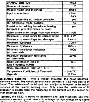
TIME K522 and K524 Sensor ConvertersThe K522 and K524 are basically operational amplifiers (high gain) used to convert resistance changes to logic levels. They can be used with variable resistance devices such as photo'conductive cells.
K578 120 VAC Input Converter
This module is used to convert 120 VAC Inputs to logic levels.
The inputs to the converters are thru transformers which provide sufficient reactive load to keep contacts clean.
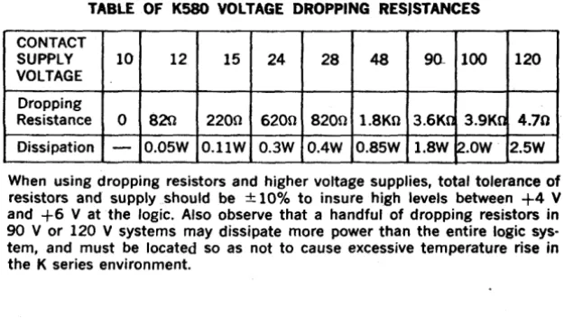
K580 and K581 Dry Contact Filters
These filters are used with wiping type switches, and provide a voltage divider t9 change a high DC voltage to K Series levels.
SWITCHl
~
OUTPUT
r~~NTACT:
WITHOUT
FILTERS ... _ _ _ "--_ _ _ _ BO_U_N_C_E _ _ ....
- TIME
SWITCHl
OUTPUT WITH
r
.FILTERS
~--~---~.~TIME
F. OUTPUT CONVERTERS-K600 GROUP
The K600 series modules are used to convert logic levels to various voltages used external to the logic system. Some of these are as follows:
K604 Isolated AC Switch
These are used to turn on and off AC devices such as solenoids, AC valves, small motors, motor starters, from logiC levels. The K604 has 4 switches, each of which can handle 200 volt-amperes. Other Isolated AC switches (K614, K615) can handle up to 500 volt-amperes.
K644 DC Driver
K671 Dec i ill a I Decoder and Nixie Display
The K67.l contains a side viewing Burroughs type nixie ,glow tube, and a
decimal decoder. The glow tube is mounted at .the end of a 12 inch flexprint cable for easy mounting. One type K771 power supply is needed for each 6 nixie displays.
G. POWER-K700 GROUP
Power is supplied to a K Series system by K Series power supply modules. K730 Rectifier for 10vdc and approx. 16vdc and sensing logic for
5vdc
K731 Rectifier
+
Regulator tor 5vdcK732 Slave Regulator
K741, K743 Power transformer
A K Series power supply is made up of a K731- and some number of K732, and K741 or K743's depending on the current requirement of the system. For example, 1 to 3 amp load requires 1 K731, 1 K732, 2 K741 or 1 K743. H. MOUNTING HARDWARE
The hardware available for K Series is very convenient.
The basic system is built from HSOO sockets (8 slots per socket) mounted on a K941 m,ounting bar, mounted on a K940 bracket, mounted on the equip-ment mounting panel. Also 19" rack assemblies are atailable with power supply (16 sockets) or without power supply (64 sockets). Also module drawers are available.
A complete line of tools is available for wire wrapping the system, along with jumpers and bus strips.
GATE EXPANDERS
\KI
'--_______ K_OO_3_,_K_Ol_2_, _KO_2_6_t K_O_2_8 _ _ _
~ ~
NEMA
I
I I
~
F
.EI H
I J
I I
:P
M LI N I P
I I
~
T $I U I V
MIL
~
1'
F E .1 . H
1 J
ffi=b
M L.1 N
1 P
ffiTI
T 5 .1 U
1 V
K003
KOO3 AND expander: May be connected to the AND expansion node of any K Series module.
NEMA
~
---
mw-~
LI M __ _
N P
I
P
T" S __ _U v . I
tS,003
MIL
:=D
E1 F
J __ 1 H
~
L , Mp ..
-1 N
:=b
1 Ts
, V __1 U
KOO3 AND/OR expander: May r,e connected to the OR expansion node of any K Series module.
KOO3-$5
KO 1 2-$8
K026-$8
NEMA Mil
K012
K012 OR expander: May be connected to the OR expansion node of any K Series module.
NEMA Mil
K026
NEMA MIL
K028
K028 AND/OR expander: May be connected to the OR expansion node of any K Series Gate.
These inexpensive gate expanders. offer great logic flexibility and versatility without a proliferation of module types. Logic functions performed byexpand-ers are illustrated in combination with the K113 and K123 gates in several pages that follow the data sheet for the gates themselves.
It 'must be clearly understood that the gate expanders above are merely ex-pansions for other K Series gates and can never be used as separate AND or OR functions.
Each K003 expander module has a .01 uf capacitor avaitable at pin B which may be used to implement logic delays as shown in the Application notes or to further reduce the speed of a K Series output.
Caution: Pin C on K028 expanders should not be' bussed to ground unless function 8-C is not used.
CABLE CONNECTOR
II
SE~ES
I
KOSO
KOSO
0 oA
0 oB
"
0 oC
0 0 0
0 oE
0 OF
0 oH
0 OJ
FLEXPRINT 0 OK
CABLE
CONNECTION 0 OL
0 OM
0 ON
0 op
0 OR
0 oS
0 OT
0 ou
0 ov
The KOSO cable connector consists of a single height, single thickness board on which can be mounted a 19 conductor fJexprint cable. Each module comes with a cable clamp for customer convenience.
/
I
LOGIC GATES
iKI
'--_ _ _
K_l_12_, _Kl_l_3_, K_l_22_,_K_12_3_, _Kl_2_4 _ _
----'
~
NEMA
NEMA
Kl12 and Kl13 INVERTING GATE
Kl22 and Kl23 NON-INVERTING GATE
32
¥IL
MIL
K112-$12 Kll~$11 K122-$13
K123-$12
NEMA
K124 AND/OR GATE
Mil
Together with the KOO3, K012, K026 or K028 expanders, these gates perform any desired logic function, including AND, OR, AND/OR, NAND, NOR, ex-clusive OR, and wired AND.
logic gate type K123 is an AND/OR non-inverting gate subject to expansion at either the AND or the OR node. logic symbols and equivalent schematics are compared in the following illustrations. Typical pin connections are shown. The AND input can be expanded up to 100 AND inputs total using pins E,l, and S. Up to 9 OR expansion inputs can be connected to the OR expansion pin (J,P, V). More OR expansion inputs can be added if faster fall times are acceptable. Both AND and OR functions can be expanded at the same time. Examples of gate expansion are shown in following pages.
Expansion of the K113 inverting gate is identical. The equivalent circuit is the same except for inversion in the output amplifier.
The K124 provides a convenient way to imptement non·inverting gate control flip-flops, exctusive ORs, and two term OR logic equations without the need for expanders. The module is electrically the same as a K123 gate with a K003 expander.
Of the three circuits on each module only one has a slowdown capacitor that c.-n be connected to the output to increase noise rejection when the gates are interconnected to make control flip-flops. Use of this capacitor in-creases rise and fall time by approximately a factor of 20. The maximum speed of each unslowed gate is 100KHz and the maximum speed of a slowed
.gat~i is 5KHz.
The K112 and K122 modules are logically identical to the K113 and K123 respectively. They feature maximum speeds of 1KHz with a single connection on one circuit for slowdown to 50 Hz. This added slowdown feature gives these two modules an even greater level of noise immunity.
· SLO~DOWN AND DELAY
To show the effects of slowdown and delay-connections on K-Series outputs, suppose a pulse entered a K123 Non-Inverting Gate: the following outputs would be reaHzed.
\ .
D
INPUT---~
CONNECT FOR
SLOWDOWN
J CONNECT .01~ f
'J
FOR DELAY CONNECT FORSLOWDOWN
J
T
CONNECT FOR DELAY .01~ fTime shown above are typical values and should not be considered exact. Delay times are increased by 10",5 for each .01",f capacitor connected to pin J.
35
NEMA H MIL NEMA MIL NEMA MIL H H H F H F H
LOGIC SYMBOL
. OR EXPANSION
INPUT
o
o
BASIC GATE
SIMPLIFIED SCHEMATIC
r - - - ,
F , +v K123 I
HI I
,..-._...:1_80
I
ID
I I
L _ _ _ _ _ _ _ _ _ _ ...l
F; - - - - -
-;oo,l
+v I
:~
----A.- -
j
F r
-HI
ID
I I
L _ _ _ _ _ _ _ _ _ _ ...l
K003 AND EXPANSION
E
F
r - - - ~K;;3""HI
+v I I _ _ -....:.,_8
0
I
10' I
L _ _ _ _ _ _ _ _ _ _ ...l
J
r - - - ~003'
F I +v I HI
I L _ _ _ _ _ _ _ J
o
NEMA
MIL
NEMA
MIL
LOGIC SYMBOL SIMPLIFIED SCHEMATIC·
F
H - -___ ~
F H F H F H 0 E F ~j F--~-"'"
H ----,~_._~
o E F H o E
r - - - ---...,
o-F ... 1 -1O--+--A,/\/Y-- +v K 123 I
H I I
1
,8
0
I 10
I I
L _ _ ~ _ _ _ _ _ _ _ .J
J
r--- ---...,
I +V K003 I
F, I
HI
L _ _ _ _ _ _ _ _ _ _ ..J
E o
. F; - _E_ -
_je: - -
-;0031
. f
I::; :1
+V :L _ _ _ _ _ _ _ _ _ _ ...J
K003 AND/OR EXPANSION (K026 MAY ALSO BE USED)
o
E
r - - - ,
F, +v K123 I
HI I
,8 0
I 1
L _______ . ___ .J
J
r---:-,
0, KO'2 I
,
I +1/
FI
I
I +V
HI
I
1+1/
L _ _ _ _ _ _ _ _ _ _ .J
The basic types of logic functions obtainable by expansion are shown below for the K123 non-inverting gate. Logic functions for the expanded K113 invert-ing gate are identical except for inversion of the output. Letters refer to logic signal names rather than module pin numbers.
A~
B~AB
~ I
BASIC NON . INVERTING GATE
A
B
c
• 0 E
F
G H
ABcDEFGH
,
I UP TO 100 INPUTS
OR EXPANSION
A B
A B
AB+CD+EF
I UP TO 9 Olt ElCPANSIOIU
.... - - -... - - UP TO 100 AND INPUTS
A B
UP TO tOO AND INPUTS
I I I
C---,,_~---,
o
E F
G K
N
o
P-"""""1L .. ~---'
R S
UP TO~OO ANOINPUTS
I
I
I
UP TO 9 .
OR EXPANSIONS
w
X
Y ~--''---_--'' : UP
1otoo
AND INPUTS(ABCOEfGH ... )+
(IJ~ .... .). (RSTUVWXYl. ... )+
NAND, NOR, EXCLUSIVE OR
The Kl13 inverting gate performs the NAND function directly, and performs the NOR function when combined with a K003 expander.
With proper input connections, the K124 non-inverting gate performs the exclusive OR function.
J
113
-AB-o-®-
B K113. ASA 8 AS
0 0
,
0 1 1
1 0 1
1 1 0
NAND FUNCTION OF BASIC INVERTING GATE
A
B
A 8
0 0 0 1 1 0
1 1 'R
1
0 0 0
·UNtJSEO INPUTS
ACT AS ONES
A+8
NOR FUNCTION OF BASIC INVERTING GATE WITH EXPANDER
A 8 A<!)B
0 0 0
0 1 1
1 0 1
1 1 0
WIRED AND
Wired AND functions can be obtained by connecting K123 outputs to -other K124, K123 or K113 outputs as shown below. Any K Series output with a fanout of 15 may be wired ANDed.
A 8 C
o
E FA8(CO+EF) A
8
C
o
E
F
WIRED AND EXAMPLES
SUMMARY Of GATE-EXPANDER LOGIC COMBINATIONS
A8(C5'+EF)
FOR ZERO VOLTS DEFINED AS FOR ZERO VOLTS DEFINED AS
lOGIC ZERO LOGIC ONE
standard definition (inverted definition)
No. No.
lo~e of
Fune on Inputs Expanders Gates Function Inputs logic of Expanders Gates
AND 2 none 1/3 K123 AND 2 1/3 KOO3 1/3 K123
3·5 1/3 KOO3 1/3 K123 3·5 or
6-8 2/3 KOO3 1/3 K123 6·9 1/3 K012
OR 2 1/3 KOO3 1/3 K123 1/3 K012 none 1/3 K124 1/3 K123
or
1/3 K012 2/3 K012 '1/3 K123
none 1/3 K124 OR 2 none 1/3 K123
3·5 1/3 K012 1/3 K123 6·9 2/3 K012 1/3 K123
3·5 1/3 KOO3 1/3 K123 6-8 2/3 KOO3 1/3 K123
NAND 2 none 1/3 K1l3 NAND 2 1/3 KOO3 1/3 K113
3·5 1/3 KOO3 1/3 K113 3-5 or
6·8 2/3 KOO3 1/3 K113 6-9 1/3 K012
NOR 2 1/3 KOO3 1/3 K113 2/3 K012 1/3 K012 1/3 K113 1/3 K113 or
1/3 K012 NOR 2 none 1/3 K113
CONTROL FLlp·FLOP FROM GATES
Control flip-flops can be formed by the interconnection of gates as shown below. For applications in systems where speeds are below 5KHz or where noisy environments exist, these flip-flops should always be slowed. When these control flip·flops are slowed, any gate output wire ANDED to them should also be slowed.
*
... --+-I OUTPUT t
0lm'UT-SET A ~
SET B
SET A SET B
NON·INVERTING GATE CONTROL FlIP·FlOP
The output of the flip·f1op above is set to a ONE when the two SET inputs are both ONEs. A ZERO at the RESET input returns the output to ZERO,
provided at least one of the SET inputs is also ZERO.
I---=-"I...:~ 0 OUTPUT
*
USE SLOWOOWN CONNECTION INFI..IP - FLOPS IF SPEED PERMITS
INVERTING GATE CONTROL FlIP·FlOP
The flip·flop above, made from two inverting gates, provides complementary 1 and 0 outputs. A truth table is shown below.
TRUTH TABLE
SET RESET 1 OUTPUT
o
OUTPUT0 0 1 1
0 1 1 0
1 0 0 1
I
~NVERTERS
11K!
/""'-_ _ _ _ _
Kl_34 _ _ _ _
---'
~
NEMA MIL
o
N ...--_. t - - - t
F
R r - -...
~-+---I
J
T r - -...
t - - - + - - t
L
K134 INVERTERS
Four flip-flop functional modules such as K210, K220, K230 can conveniently be augmented by a K134 to get "0" as well as "1" outputs. The KI34 is also provided with expansion and inhibit inputs for use 8S the readout· ele-ment of ready-only memories using K281 diode memories (See Applications Notes). A common input at pin K can force all four outputs high, a helpful feature for building large K281 memories or very large K161 decoders. Kl34 inverters may also be AND expanded by K003 gate expanders, provid-ing an efficient way to obtain 4-input NAND or inverted NOR gates.
INVERTERS
I~
'---_ _ _ _ _
K_l_35 _ _ _ _ _
...
~
NEMA MIL
I; K
K135 INVERTERS
The K135 module was designed primarily for use in applications that require inverters with "OR" expandability. A common input at pin K can force all four outputs high regardless of the "OR" gate inputs. This feature is useful if a K161 decoder is used for multiplexing K135 modules, since all outputs for the same bit can be wire "AND"ed together.
The loading on pin K is initially 6 with no "OR" expansions and increases by "I" unit load for each "OR" input that is added to the module. For example, if a K012 expander was added to each of the four inverters, the total pin
K.
load would be 22 unit loads.
"KOO3 expanders can be used for AND/OR expandability. The number of AND inputs on a given OR input does not affect the loading of ,pin K.
INVERTERS
II
S~ES
I
K138NEMA MIL
~
~
~
~
~
~
2 15
~
~
~
~
2 t5~
2 t5~
~
~
~
~
The K138 has eight inverter circuits on each module. These circuits can be· used to invert other K Series outputs to obtain both a high (+5V) level as well as a low (ov) level. The K138 is pin compatable with the Kl34 and K135 and m8¥ be substituted for. them if a higher density of inverters is desired.
BINARY TO OCTAL DECODER
I
SE~ES
I
K161
CONN.ECT TO SLOW
B
I / DOWN ZERO OUTPUT
I
0 I
0
F 15
2 J 15
3 L 15
2·
N
4 15
4
5 R 15
T
6 15
V
INH 7 15
K161 DECODER
Three-bit binary numbers at the input to the K161 will be decoded into eight one-at-a-time outputs. Both inputs and outputs are high for assertion. The inhibit input allows BCD to ten line decoders to be built, or permits several decoders to be interconnected for sixteen, twenty-four, thirty-two outputs, etc. The inhibit may be left open if unused, even though high is the inhibit state. When the K161 is being used with M series, all input signals must be buffered with K series gates. ",:his is necessary due to the 3 volt thresholds in the KI61. Standard K Series slowdown circuits on each output minimize and for most purposes nullify the splinter pulses that all decoders emit during input tran-sitions. Additional slowdown available on the zero output can usually suppress the larger splinter that may occur there. But since splinter size is ultimately determined by input timing tolerances, it is cleanest to avoid logic designs in which a decoder output is used as a source of pulses.
The diagrams below show how to connect decoders for 8, 10, 16 and 32 out-puts. Much larger decoders are possible, and in fact up to 256 outputs or even more can be obtained by inhibiting all but one of several decoders.
8 STATE DECODER
7 6- 5 4 3 2 1 0
BINARY-COOED-DECIMAL (BCD) DECODER
Q
2
M
3
p 4
S 5
6 U
7
8 '6
9 10 M
11
P 12
S 13
14
U
15·
16
17
18 M
f9
P 20
S 21
22
U
23
24 16
25
26
M
27
P 28
S 29
30, U
31
EQUALITY COMPARATOR
~
""--' _ _ _ _ _ _ K_17_1 _ _ _ _ _ ----'
~
NEMA MIL
oJ
The K171 is a four bit equality comparator whose output at pin J is high if the two numbers being compared are equal. Pins N, R, T, and V are compared with pins M, P, S, and U. The output, Pin
J,
has no drive capability and mustbe connected to the AND expansion node of either a Kl13 or K123 logic gate. More than 4 bits can be compared using any number of K171 's, by tying all K171, pin J, outputs together at the same AND expansion node.
K210
This module- can be used. in conjunction with the K174 to obtain the three independent outputs for greater-than, less-than, and equal-to.