SRAM Cell Performance in Deep Submicron Technology
Sampath Kumar
J.S.S. ATE, noida, India,Sanjay Kr Singh
IPEC, Ghaziabad, IndiaD. S. Chauhan
UTU, Dehradun, India
B.K.Kaushik
Arti Noor
IIT Roorkee, India C-DAC, Noida, India,
ABSTRACT
This paper deals with the design opportunities of Static Random Access Memory (SRAM) for lower power Consumption and propagation delay .Here we have analyzed both read margin for read ability and write margin for SRAM write ability. Static Noise Margin affects both read margin and write margin. We have analyzed the Static Noise Margin using traditional butterfly method which requires the rotation of VTC by 45 degrees. SRAM cell is analysed through the considering of different type of analysis such as Static Noise Margin, Data Retention Voltage, Read Margin and Write Margin in 350nm technology.
Keywords
SRAM, SNM, DRV, SOC, CMOS, DIBL
1.
INTRODUCTION
As the time passes the semiconductor electronics has been desire to miniaturize the components, improve their reliability and reduce the size of system. To improve this quality of semiconductor electronics, it is necessary to compare the devices. During the comparison we can see that which device has better performance and reliability. All of these goals can be achieved by integrating more and more components on the same die to include increasingly complex electronic functions on a limited area with minimum weight, reduced system cost, improved performance and also the stability of the cell. Static Noise Margin (SNM) is used to measure of cell stability. Also an important factor on which the cell performance depends is DRV which is minimum voltage required to retain the data. For improving this property the design process depends on certain parameters such as temperature, channel width etc...
In last few years, significant progress has been made in design and development of low power electronics circuits. Power dissipation has become a topic of intense research and development of portable electronic devices and systems. In VLSI chip, with higher levels of integration, packaging density of transistors is increasing. As a result, for high levels of integration power dissipation becomes the dominant factor. CMOS technology is known for using low power at low frequency with high integration density. There are two main components that determine the power dissipation of a CMOS gate, first component is the static power dissipation[9] due to leakage current and second component is the dynamic power dissipation [10] due to switching transient current and charging/discharging of load capacitance. In order to accurately determine the heat produced in a chip, one must determine the power dissipated by the number of gates and the
devices, microprocessors, DSP’s and embedded throughput. Hence low power design of digital integrated circuits has emerged as a very active enveloping field. As integrated chip designers accelerate their adoption of today’s deep sub micron Semiconductor (DSM) technologies, squeezing the maximum transistor count into and the maximum performance, minimum power and noise out of their high performance designs, increasing importance is placed on the accuracy of cell characterization systems.
In this paper we are mainly concentrated on the comparison between various parameters of 6T & 14T SRAM cells. In section 2, the SRAM cell designopportunities, failure type of SRAM cell and operation of 6T cells are explained and section 3 contain operation of 14T cells. In section 4, the SRAM cell Static noise margin (SNM) simulation is explained and in section 5, data retention voltage (DRV) is explained. Lastly the SRAM cell summary of simulated result is explained in section 6.
2.
SRAM CELL DESIGN OPPORTUNITIES
The 6T SRAM, which continues to play a dominant role in future technology generations because of its combination of density, performance, and compatibility with logic processing. The successful commercial scaling of the 6T SRAM driven by strong industry competition is expected to continue beyond different technologies. Also the area reduction is important factor for cell design. During the chip design 6T cells are considered because of the commercial success of the 6T SRAM. The failure mechanisms of large memory arrays will extend the life of the 6T SRAM in VLSI circuits. The fail types for SRAM arrays may be divided into two distinct categories:
(i) hard fails i.e., those attributable to defects
Operation of 6T SRAM
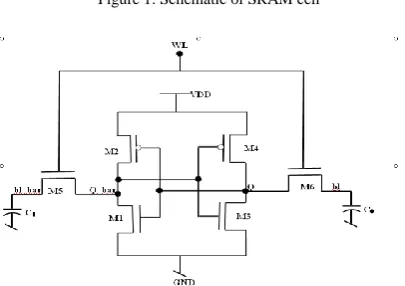
[image:2.595.62.265.142.285.2]The figure 1 given below shows the schematic of 6T SRAM cell which has two modes of operation: retention mode and access mode.
Figure 1: Schematic of SRAM cell
During retention mode, the WL signal is deactivated and the storage nodes are isolated from the bitlines. The latch action during this mode helps retain data as long as the cell is powered with very low static power consumption. The cell enters access mode when the WL signal is activated. The \on" access transistors allow the cell to communicate with the bitlines. The bitline/storage node interaction depends on the intended operation. If a read operation is intended, the bitlines transfer data from the cell's storage nodes to the outside world. On the other hand, the bitlines transfer data from the outside world to the cell's storage nodes when a write operation is forced by a low-impedance write driver.
3.
14 T SRAM cell
The 14T [15] memory cells are shown in Figure2. The two NMOSes or PMOSes connect the internal nodes in the pair of memory cells (―N00 and N10‖, ―N01 and N11‖) respectively. That’s why, we name these memory cells 7TN cells and 7TP cells. Compared with the conventional 6T memory cell the respective area overhead are 26% and 11%, in the case of logic design rule. A pair of 7TN is 14TN and a pair of 7TP is 14TP, which are for the high speed and dependable modes.
Figure2:14T SRAM Cell
The proposed 7T/14T memory cell has three modes of operation:
Normal mode (7T): The additional transistor are turned off (CTRL=‖L‖ or/ CTRL="H‖) and the 7T cell act as conventional 6T cell.
High speed mode (14T): The additional transistor are turned on (CTRL=‖H‖ or/ CTRL=‖L‖) and the internal nodes are shared by the memory cell pair. Both WL [0] and WL [1] are driven which enables faster readout using 14Transistor.
Dependable Mode (14T): The additional transistor is activated but either WL [0] or WL [1] is asserted. By doing so, a larger static noise margin can be obtained because a β ratio is doubled.
In the normal mode one bit data is stored in one memory cell, which is the most area efficient. In the high speed mode the dependable mode, one bit data is stored in two memory cells although the quality of the information is different from the normal mode. The ―higher speed‖ or ―more dependable‖ information can be obtained. We call this concept ―quality of a bit (QOB)‖. The quality of the information is scalable in our proposed memory cell.
4. STATIC NOISE MARGIN (SNM)
SIMULATION
Static Noise Margin (SNM) is a stability metric of an SRAM cell. The SNM can be graphically represented as the largest square between the voltages transfers characteristic (VTC) curves of the internal inverters. Some important results that are observed from simulation of the schematic designed in IC Flow are summarized below. Wehave taken of cell ratio vs. static noise margin, then the value of static noise margin increases with the increase of cell ratio of the SRAM cell in 350nm technology. If the value of the driver transistor increased then Cell ratio (CR) also increased. Hence current is increased then speed is also increased.
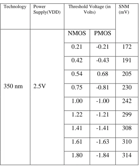
4.1 Threshold Voltages vs. SNM
Table 1 given below shows the threshold Vs SNM for NMOS
Table 1: Threshold Voltage (VT) Vs SNM
Technology Power Supply(VDD)
Threshold Voltage (in Volts)
SNM (mV)
350 nm
2.5V
NMOS
PMOS
0.21
-0.21
172
0.42
-0.43
191
0.54
0.68
205
0.75
-0.81
230
1.00
-1.00
242
1.22
-1.21
299
1.41
-1.41
308
1.61
-1.63
310
[image:3.595.58.280.426.585.2]1.80
-1.84
314
Figure 3: SNM Vs Threshold voltage for NMOS & PMOS
4.1 CR Vs SNM and PR Vs SNM:
The table2.a given below shows the CR Vs SNM and table2.b shows the PR Vs SNM for the 350 nm technology and 2.5V supply voltage. We can see in table2 that SNM for read increases with increase of CR and SNM for write also increase with increase of PR. CR(Cell ratio) increases means the size of driver transistor increases and when the PR (Pull Ratio) increases means the size of load transistor also increases.
Table2.a: CR vs. SNM (Read)
Technology Power supply VDD
Cell Ratio (CR)
Width of Transistor (M2) (in µm)
Read SNM
(mV)
350nm 2.5mv
0.35
0.7
350
0.5
1.0
356
0.7
1.4
360
1.0
2.0
364
1.4
2.8
370
Table2.b: PR Vs SNM (Write)
Technology Power supply VDD
Pullup Ratio (PR)
Width of Transistor (M3) (in µm)
Write SNM (mV)
350nm 2.5mv
0.35
0.7
350
0.5
1.0
356
0.7
1.4
360
1.0
2.0
364
1.4
2.8
370
Figure 4(a) given below shows that the SNM and transistor width increases as the CR increases and figure 4(b) shows that SNM and transistor width also increases with increase in PR.
Figure 4: (a) shows CR VS read SNM (b) PR VS write
SNM
[image:3.595.315.546.548.688.2]5. DATA RETENTION VOLTAGE (DRV)
The term DRV refers to data detention voltage, for each SRAM cell there is a data-retention-voltage above which the data bit (0 or 1) is stored reliably.
[image:4.595.55.284.330.444.2]To determine the optimal standby VDD of an SRAM, it is important to understand the voltage requirement for SRAM data retention. In 350 nm technology the power supply voltage is 2.5V.Then decrease the power supply voltage until the flip the state of SRAM cell. If Q=1, Q’=0, it is changes the value of Q=0, Q’=1. I took the value of power supply voltage up to 0.2V then it is change the state of cell. We know, Minimum power supply voltage to retain high node data in the standby mode: Vdr=Vdd=0.2V for 350 nm Technology. Some important results that are observed from simulation of the schematic designed in IC Flow are summarized below: Data Retention voltage also affects on the SNM of the SRAM cell. It is important parameter for the saving supply voltage. SNM decreases with the decrease in value of the data retention voltage. Data retention voltage should be greater than threshold voltage. Data retention voltage is greater than the threshold voltage is shown in figure 5.
Figure 5: DRV Vs SNM (350nm)
5.1 CR Vs Read margin and PR Vs Write
margin:
In the table 3 given below shown CR Vs Read margin and PR Vs Write margin for 350nm technology. Table2 shows that Read margin increases with increase in CR and Write margin also increases with increase in PR which is also clear in figure 6(a) and 6(b).
Table 3: CR Vs Read Margin & PR Vs Write Margin at 350nm technology
Technology CR Read
Margin
PR Write
Margin
350nm
0.5
0.7
2.5
0.25
0.7
0.75
3.0
0.4
0.8
0.8
3.5
0.6
1.0
0.9
4.0
0.75
Figure6: (a) shows CR VS read margin (b) shows PR VS
write margin
(a) (b)
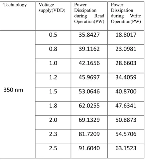
5.3 Power Dissipation:
[image:4.595.310.548.397.660.2]
Some amount of power is dissipated during read and writes operation .Table 4 shows the variation of power dissipation during Read and Write operation with supply voltage. We can observe from table that as the supply voltage increases the power dissipation for Read and write also increases. It can clearly see in the figure 7 which shows the plot between supply voltage and power dissipation for Read and Write.
Table 4: power Dissipation during Read Operation and Write Operation
Technology Voltage supply(VDD)
Power Dissipation during Read Operation(PW)
Power Dissipation during Write Operation(PW)
350 nm
0.5
35.8427
18.8017
0.8
39.1162
23.0981
1.0
42.1656
28.6603
1.2
45.9697
34.4059
1.5
53.0646
40.8700
1.8
62.0255
47.6341
2.0
69.1329
50.8873
2.3
81.7209
54.5706
Figure 7: Supply voltage Vs Read and Write power dissipation
6.
SUMMERY
OF
SIMULATED
RESULTS:
Results that are observed from simulation of the schematic designed in IC Flow are summarized below:
Table 5: CR vs. SNM (Comparison of 6T and 14T)
Technology Power Supply (VDD)
Cell Ratio (CR)
Width of Transistor
(M2) (in μm)
SNM (mV) (14T)
SNM (mV) (6T)
350 nm
2.5V
0.35
0.81
352
81.0
0.51
1.00
361
93.0
0.73
1.43
364
101.7
1.00
2.01
368
105.1
1.41
2.83
370
109.0
[image:5.595.58.285.107.288.2]Table 5 shows the width of transistor and SNM for 14T & 6T using 350nm technology and 2.5 V supply voltage. We can see that the SNM and width of transistor increases with increase in CR. It is also clear from figure 8 which shows the comparison between 14T and 6T SRAM cell for common cell ratio.
Figure 8: CR Vs SNM for 14T & 6T
Here the table given below shows the DRV VS SNM for 14T
and 6T
Table 6: DRV vs. SNM (Comparison of 6T and 14T)
Technology Power supply voltage(VDD)
DRV SNM
(mV)(14T) SNM (mv)(6T)
350 nm 2.5V
0.2
17
27
0.3
33
56
0.4
69
73
0.5
100
85
0.6
119
88
0.8
132
90
1.0
141
91
1.4
154
93
1.7
161
94
2.1
299
104
2.5
418
211
Figure 9 given below shows the plot of table 6 which indicate that the ratio of SNM increasing is faster in 14T as compared to 6T.
[image:5.595.309.547.121.410.2] [image:5.595.60.287.616.749.2]Table 7 shows the PR Vs write margin for 350nm technology
and also compare the SNM for 14T & 6T and figure 10 shows the plot between PR and SNM.
Table 7: Write Margin vs. SNM (Comparison of 6T and 14T)
Technology PR Write margin
SNM (mv) 14T
SNM (mv) 6T
350nm
2.5
0.26
345
105.1
3.0
0.42
355
106.6
3.5
0.61
365
207.9
4.0
0.75
370
210.5
Figure10: PR VS SNM for 14T & 6T
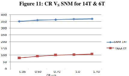
Similarly table 8 shows the CR Vs Read margin for 350nm technology and also compares the SNM for 14T & 6T and figure 11 shows the plot between CR and SNM .
Table 8: Read Margin vs. SNM (Comparison of 6T and 14T)
Technology CR Read
Margin
SNM (mv) 14T
SNM (mv) 6T
350nm
0.35
0.3931
352
81
0.50
0.3983
361
93
0.70
0.4010
364
101.7
1.00
0.7001
368
105.1
[image:6.595.325.540.129.255.2]1.40
0.7019
370
109
Figure 11: CR VS SNM for 14T & 6T
Finally, the different type of analysis of SRAM cell using different method in 350nm technology through which we can find out which method has better performance. When we use butterfly method for the analysis of SNM, it would be high, the value of SNM will approx 533mv for Vdd=2.5v. The method decreasing power supply voltage for the analysis of DRV, it should be larger than threshold voltage and approx 0.37253370, similarly for write margin we are using BL swapping method and got the value 0.3071v and we conclude that larger write margin larger write ability. At last when we use traditional SNM (Butterfly method) for the read margin analysis we get the value 0.1315v and conclude that read margin is less than the write margin.
7. CONCLUSION:
8. REFERENCES
[1] K. Zhang, U. Bhattacharya, Z. Chen, F. Hamzaoglu, D. Murray, N. Vallepali, Y. Wang, B. Zheng, and M.Bohr. A 3-GHz 70-Mb SRAM in 65-nm CMOS technology with integrated column-based dynamic power supply. IEEE Journal of Solid State Circuits (JSSC), 41:146– 151, January 2006.
[2] A. Bhavnagarwala, X. Tang, and J. Meindl. The impact of intrinsic device fluctuations on CMOS SRAM cell stability. IEEE Journal of Solid-State Circuits (JSSC), 36:658–665, April 2001.
[3] F. Lai and C. Lee. On-chip voltage down converter to improve SRAM read-write margin and static power for sub-nano CMOS technology. IEEE Journal of Solid-State Circuits (JSSC), Vol 42, Issue -9, :2061–2070, Aug 2007.
[4] M. Horiguchi, T. Sakata, and K. Itoh, "Switched-source-impedance CMOS circuit for low standby subthreshold current giga-scale LSI's," IEEE Journal of Solid-State Circuits, vol. 28, issue 11, pp. 1131-1135, Nov. 1993. [5] B. H. Calhoun, A. Chandrakasan, "A 256kb sub-threshold
SRAM in 65nm CMOS," IEEE International Solid-State Circuits Conference, pp. 628, Feb 2005.
[6] Andrew Carlson,Zheng Guo,Sriram
Balasubramanian,Radu latanovici,Tsu-Jae King Liu, and Borivoje Ni•Z. Guo, S. Balasubramanian, R. Zlatanovici, T. King Liu, and B. Nikolic, "FinFET-based SRAM design," in Proc. ISLPED '05, Piscataway, NJ: IEEE, 2005, pp. 2-7
[7] H. Mizuno and T. Nagano, "Driving source-line (DSL) cell architecture for sub-1-V High-speed low power applications," Digest of Technical Papers. Symposium on VLSI Circuits, pp. 25–26, June 1995.
[8] H. Kawaguchi, Y. Iataka, and T. Sakurai, "Dynamic Leakage Cut-off Scheme for Low-Voltage SRAM's,"Digest of Technical Papers, Symposium on VLSI Circuits, pp.140-141, June 1998.
[9] F. Li, D. Chen, L. He, and J. Cong, ―Architectureevaluation for power-efficient FPGAs,‖ In Proceedings of ACM International Symposium on Field Programmable Gate Arrays, 2003, 175—184.Feb 2002. [10] L. Shang, A. S. Kaviani, and K. Bathala, ―Dynamic
power consumption in Virtex-II FPGA family,‖ in FPGA '02 Proceedings of the 2002 ACM/SIGDA tenth international symposium on Field-programmable gate arrays – pp 157-164.
[11] Avant Star-Hspice Manual Volume III- MOSFET Models 1999-2000 A. Keshavarzi, S. Ma, S. Narendra, B. Bloechel, K. Mistry, T. Ghani, S. Borkar, and V. De,―Effectiveness of Reverse Body Bias for Leakage Control in Scaled Dual Vt CMOS ICs,‖ Proceedingsof the International
Symposium on Low Power Electronics and Design (ISLPED), Huntington Beach, CA, August 2001, pp.207–212. [12] K. Flautner et al, "Drowsy caches: simple techniques for
reducing leakage power," International Symposium on Computer Architecture, pp. 148-157, May 2002. [13] J. Lohstroh, E. Seevinck, and J.D. Groot, "Worst-Case
Static Noise Margin Criteria for Logic Circuitsand Their Mathematical Equivalence," IEEE Journal of Solid-State Circuits, vol. SC-18, no. 6, pp.803-807, Dec 1983. [14] Sanjay Kr Singh, Sampath Kumar, Arti Noor, D. S.
Chauhan & B.K.Kaushik.
―International Journal of Advances in Engineering & Technology‖, Vol. 1, Issue 5, pp.429-436,Nov 2011. [15]A dependable SRAM with 7T/14T memory cell by
Hidehiro Fujiwara published in ―IEICE TRANS ELECTRON VOL E92-C, No.4 April 2009‖