Designing a Novel Power Efficient D- Flip-Flop using
Forced Stack Technique
Karna Sharma
Department of Electronics and Communication Maharaja Surajmal Institute of
Technology New Delhi, India
Manan Sethi
Department of Electronics and Communication Maharaja Surajmal Institute of
Technology New Delhi, India
Paanshul Dobriyal
Department of Electronics and Communication Maharaja Surajmal Institute of
Technology New Delhi, India
ABSTRACT
In Integrated circuits a gargantuan portion of on chip power is expended by clocking systems, which comprises of timing elements such as flip-flops, latches and clock distribution network. These elements absorb approximately 30% to 60% of the total power dissipation in the system. In order to design high performance and power efficient circuits a scrupulous approach should be adopted to reduce the power consumed by flip-flops and latches. In this paper various power efficient flip- flops with low power clock distribution network are examined. Among these flips-flops low Power Clocked Pass Transistor Flip-Flop (LCPTFF) consumes least power than Clocked Pair Shared Flip-Flop (CPSFF), Conditional Data Mapping Flip-Flop and Conditional Discharge Flip-Flop (CDFF). We propose a novel Low Power Forced Stack Clocked Pass Transistor Flip-Flop (LP-FSCPTFF) which reduces the power consumption by approximately 30.1% to 83.93% at 500MHz and 25.5% to 90.1% at 750MHz as compared to original LCPTFF. The simulation is carried out on Tanner EDA v13.0 at 90nm on different voltages at 500MHz and 750MHz. The temperature variation of different flip-flops is also shown at 5 °C, 2 5 °C and 50 °C.
General Terms
Power Consumption, Temperature
Keywords
Flip-Flops, Forced Stack Approach, Low power integrated circuits.
1.
INTRODUCTION
The SYSTEM ON CHIP (SOC) design integrates millions of transistors on a single chip as a result there is a colossal amount of power dissipation taking place in the circuit [1]-[5]. Earlier the VLSI designers were more inclined towards dwindling the area and enhancing the computational speed of the circuits, whereas the power consumption was an inconsequential factor. Recent years, have shown that power consumption is equally important in comparison to area and speed to devise a high performance circuit. With ever
increasing demand of handheld portable devices, Personal Digital Assistance and Personal Communication devices, reducing the on-chip power consumption plays a pivotal role in increasing the battery life.
The four indispensable components comprising the total power dissipation in an integrated circuit are [2]:-
(1)
PTotal is a termed coined for total power dissipation, which constitutes Ileakage,Isc and Ist currents and switching power dissipation. In equation (1), αCLVdd2
fclk corresponds to the power dissipation during switching event, where CL is coined for the load capacitance; fclkis the clock frequency and α denotes the node transition factor. The second component corresponds to the short-circuit current, Isc, which appears when both pMOS and nMOS transistors conducts in parallel for a transparency period, setting up a direct current path from power supply to the ground. The leakage current, Ileakage, in the circuit is repressed by two indispensable sub-threshold leakage current and the other one is the reverse diode leakage current during fabrication process. The static current, Ist, is the direct current from power supply.As the circuit designing takes place at lower technology, short-circuit and leakage power then becomes an important part along with the dynamic power dissipation. One of the effective approaches to abate the leakage power consumption along with retention of the logic state is the Forced Stack technique [6],[7]. Thus designing a flip-flop using this technique will have a humongous effect on integrated circuits.
This paper is organized as follows. Section 2 surveys various low power clocking flip-flops. Section 3 describes Forced Stack technique to reduce sub-threshold leakage power consumption. Section 4 presents the proposed low Power Forced Stack Clocked Pass Transistor Flip-Flop(LP-FSCPTFF)for low power and better performance. Section 5 presents simulation results. Section 6 represents the conclusion.
Geetanjali Sharma
Department of Electronics and Communication Maharaja Surajmal Institute of
2.
VARIOUS LOW POWER CLOCKING
FLIP-FLOPS
There are various genres of D flip-flops and they are categorized as: conditional discharge flip-flop (CDFF), conditional data mapping flip-flop (CDMFF) and clocked pair shared flip-flop (CPSFF) and low power clocked pass transistor flip-flop (LCPTFF).
CDFF works for both implicit as well as explicit pulse triggered flip-flop systems. In CDFF as shown in the Figure 1(a) [8], a special pulse generator circuit is used which generates clock pulse that help us to trigger the circuit at both positive and the negative edges as a result the whole system works on double edge triggered technology [9]. In CDFF the redundant switching activity is minimized by controlling the discharge path by using anMOS transistor at the bottom which is driven by input Qb. The CDFF works in two modes first is the low to high transition when input is high, and the second is the high to low transition when input becomes low. The CDFF reduces the power dissipation by incorporating double edge triggered technology but area is increased by using an explicit pulse generator circuit.
The CDMFF shown in the Figure 1(b) [8] incorporates conditional data mapping (CDM) technology. In the flip-flops when the inputs are (0, 0) memory state is retained that is Q and Qb retains their present values. The CDMFF exploits this property of the flip-flops by mapping the inputs back to (0, 0) when any kind of redundant switching event is predicted by using Q and Qb as the control signals. All this is established with the help of a data mapping circuit. The CMFF is a pulse triggered flip-flop and does not work on double edge triggered technique. The major advantage of CDMFF is that reduces the clock load by using 7 clocked transistors in comparison with CDFF which uses 13 clocked transistors as a result there is a reduction in the power dissipation in CDMFF. The D to Q delay of CDMFF is better as compared to CDFF [10]-[12]. The major disadvantages associated with CDMFF are that it is more prone to redundant switching events with the presence of a floating node in the circuit Figure 1(c) [8]. The CPSFF overcomes the problem of the floating node by grounding the M1 pMOS transistor thus charging the internal node through Vdd in Figure 1(c). In CPSFF the two nMOS transistors M5 and M6 are clocked paired which is shared by the first and the second stage.
The CPSFF works when both clk and clk bar are 1. For input D= ‘1’, assuming Q= ‘0’ and QB= ‘1’ the nMOS M3 will be on and M8 will be off. Thus a direct path from ground is available. In the second stage, Q= ‘1’ and QB= ‘0’.
The CPSFF uses 4 clocked transistors in comparison with CDMFF which uses 7 clocked transistors thus reducing the power dissipation and the area [10]. However, CPSFF experiences noise coupling at higher frequencies which makes the analysis a bit tedious [13].
(a)
(c)
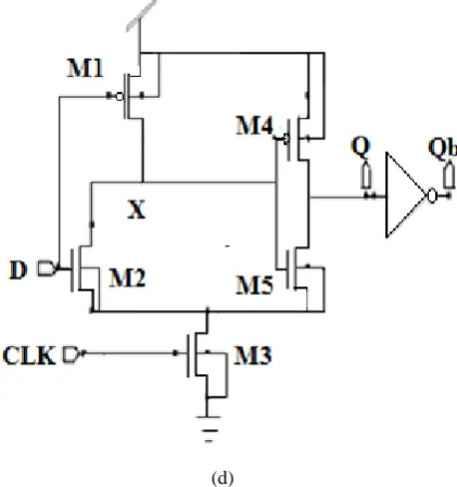
The LTCPFF reduces the clocked load by using a single clocking transistor as compared to 4 clocking transistor in CPSFF and 7 clocking transistor in CDMFF. This reduces the power dissipation by a prodigious amount as compared to CDFF, CDMFF, and CPSFF [10]. The LTCPFF, shown in Figure 1(d) employs pass transistor logic and uses only 7 transistors including the not gates which results in the reducing the area by considerable amount. In LTCPFF when D = ‘1’ and CLK = ‘1’ then M2, M3 is on and M1 is off as a result node x discharges through the ground hence M4 is on and Q attains a high logic. When D = ‘0’ then M1 is on hence node x charges through Vdd as a result M4 is off and M5 is on and Q attains logic low.
(d)
Fig. 1: (a) CDFF (b) CDMFF (c) CPSFF (d) LCPTFF
3.
FORCED STACK TECHNIQUE
Sub-threshold leakage current increases whenever there is abatement in the threshold voltage. Major challenge faced by the technology scaling is the mercurial proliferation of the sub-threshold leakage power due to subdued threshold voltage. Hence, this leakage power component needs to be reduced in such systems and thus it becomes highly crucial to formulate a technique for its reduction.
[image:3.595.69.274.75.358.2]There are several techniques in the literature for the reduction of the leakage power and one of them is to stack the transistors [14]. The stacking of transistors results in the subjugation of sub-threshold leakage current by simultaneously turning off two or more transistors Figure 2 [6].
Fig. 2: Forced Stack Technique
Here in the Figure 2, because of the two nMOStransistors the current flow delay increases which subdues the circuit's leakage power.
The forced stack technique incorporates a stack by resolving an existing transistor into two transistors half of its size. The forced stack approach retains the logic state by saving the huge leakage power. Byturning off the two transistors at the same time, a reverse bias is induced between those two transistors which ultimately results in the subjugation of subthreshold leakage current.
The foremost disadvantage of this technique is the momentous enhancement of delay time which confines the application of this technique.
4.
PROPOSED DESIGN USING FORCED
STACK TECHNIQUE
[image:3.595.330.538.237.476.2] [image:3.595.64.275.512.737.2]voltage to the stacked transistors result in making them off and abatement of sub-threshold leakage power.
When clock = ‘0’ then both the stacked nMOS transistors M5 and M6 are off and this results in low leakage power. When clock=‘1’ and D=‘1’; then M3, M5 and M6 is on and M1 is off as a result node x discharges through the ground hence M2 is on and Q attains a high logic.
[image:4.595.59.274.269.546.2]Albeit the number of clock transistors is increased from 1 to 2 as compared to LTCPTFF and the total numbers of transistors are increased from 7 to 8, there is only a diminutive increase in area with a profound reduction in the power consumption. The proposed flip-flop operates at different temperatures with the same consistency and shows better result than the other low power clocking flip-flops.
Fig. 3: Low Power Forced Stack Clocked Pass Transistor flip-flop (LP-FSCPTFF)
5.
SIMULATION RESULTS
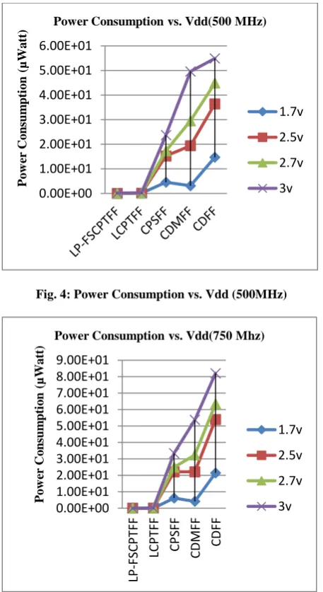
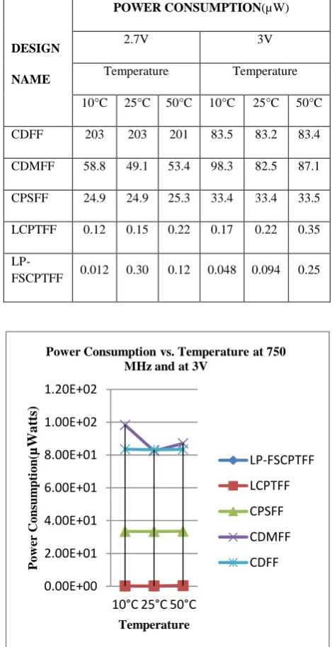
The results simulated for various low power clocking flip-flops and for our proposed flip-flop design were obtained on Tanner EDA Tool 13.0v over various supply voltages, temperatures and frequencies by using the 90nm CMOS technology as shown in Table 1, 2& 3. Table 1 shows power consumption values for CDFF, CDMFF, CPSFF, LCPTFF and our proposed design LP- FSCPTFF obtained on different set of voltages at 500MHZ and 750MHz.The power consumed by CDMFF when compared with CDFF is 80.6% less for 1.7v at 750MHz as shown in Figure 4. The CDMFF is overshadowed by CPSFF in terms of power consumption showing a 52.2% reduction in power consumption for 3v at 500MHz. This subjugation in the power is a result of reduced number of clocking transistors that is in case of CPSFF only 3
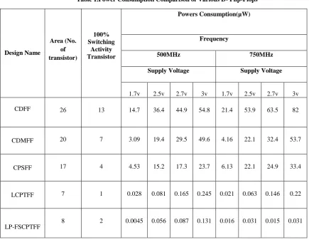
[image:4.595.314.543.328.747.2]clocked transistors are employed in comparison to CDMFF which uses 7 clocked transistors. The CPSFF is outshined by LCPTFF in terms of power consumption by showing a 99.37% reduction in power consumption for 1.7v at 500MHz as shown in Figure 5. This suppression in the power is a result of reduced number of clocking transistors that is in case of LCPTFF only 1 clocked transistor are employed in comparison to CPSFF which uses 4 clocked transistors. In Table 1 our proposed design i.e. LP-FSCPTFF when examined on 2.5v for 500MHz the power is reduced to 30.1% and the same circuit when examined on 1.7v for 500MHz the reduction is 83.93% as compared to the power consumption values for LCPTFF at the same set of conditions.LP-FSCPTFF when examined on 1.7v for 750MHz the power is reduced to 24.5% and the same circuit when examined on 2.7v for 750MHz the reduction is 90.1% as compared to the power consumption values for LCPTFF at the same set of conditions. Similarly, our proposed LP-FSCPTFF outshined other mentioned flip-flops in terms of power consumption over a temperature range as shown in Figures 6 & 7.
[image:4.595.315.541.333.521.2]Fig. 4: Power Consumption vs. Vdd (500MHz)
Fig. 5: Power Consumption vs. Vdd (750MHz) 0.00E+00
1.00E+01 2.00E+01 3.00E+01 4.00E+01 5.00E+01 6.00E+01
Po
w
er
Co
n
sum
p
ti
o
n
(
µ
W
a
tt)
Power Consumption vs. Vdd(500 MHz)
1.7v
2.5v
2.7v
3v
0.00E+00 1.00E+01 2.00E+01 3.00E+01 4.00E+01 5.00E+01 6.00E+01 7.00E+01 8.00E+01 9.00E+01
LP
-FSC
PT
FF
LCPT
FF
CPSF
F
CD
MFF CDFF
Po
w
er
Co
n
sum
p
ti
o
n
(
µ
W
a
tt)
Power Consumption vs. Vdd(750 Mhz)
1.7v
2.5v
2.7v
Table 2. Power Consumptionvs.Temperature (500MHz)
DESIGN
NAME
POWER CONSUMPTION(µW)
2.7V 3V
Temperature Temperature
10°C 25°C 50°C 10°C 25°C 50°C CDFF 44.6 44.9 45 57.2 56.7 57.5 CDMFF 50 42.6 47.9 84.7 73.4 78.9 CPSFF 18.2 17.3 17.5 23.5 23.7 22.1 LCPTFF 0.135 0.165 0.239 0.192 0.245 0.369
LP-FSCPTFF 0.1 0.124 0.197 0.174 0.209 0.341
Fig. 6: Power Consumption vs.Temperature (500MHz) Design Name
Area (No. of transistor)
100% Switching
Activity Transistor
Powers Consumption(µW)
Frequency
500MHz 750MHz
Supply Voltage Supply Voltage
1.7v 2.5v 2.7v 3v 1.7v 2.5v 2.7v 3v
CDFF 26 13 14.7 36.4 44.9 54.8 21.4 53.9 63.5 82
CDMFF 20 7 3.09 19.4 29.5 49.6 4.16 22.1 32.4 53.7
CPSFF 17 4 4.53 15.2 17.3 23.7 6.13 22.1 24.9 33.4
LCPTFF 7 1 0.028 0.081 0.165 0.245 0.021 0.063 0.146 0.22
LP-FSCPTFF 8 2 0.0045 0.056 0.087 0.131 0.016 0.031 0.015 0.031
0.00E+00 1.00E-05 2.00E-05 3.00E-05 4.00E-05 5.00E-05 6.00E-05
10°C 25°C 50°C
Po
w
er
Co
n
sum
p
ti
o
n
(
µ
Wa
tt
)
Temperature
Power Consumption vs. Temperature at 500 MHz and at 2.7V
LP-FSCPTFF
LCPTFF
CPSFF
CDMFF
[image:5.595.313.551.511.724.2]Table 3. Power Consumptionvs.Temperature (750MHz)
Fig. 7: Power Consumption vs. Temperature (750MHz)
6.
CONCLUSION
In this paper the proposed D Flip-Flop results in the subjugation of both redundant switching and sub-threshold leakage current by incorporating forced stack technique. The LP-FSCPTFF at 500MHz is able to reduce the power consumption by approximately 30.1% to 83.93% in comparison with the LCPTFF .At 750MHz the power consumption of LP-FSCPTFF is reduced by approximately 25.5% to 90.1% in comparison with the LCPTFF. The proposed Flip-Flop can be used for making synchronous as well as asynchronous registers, counters, SRAMs, DRAMs etc.
7.
REFERENCES
[1] M. Pedram, “Power minimization in IC Design: Principles and applications,” ACM Transactions on Design Automation of Electronic Systems, vol. 1, pp.3-56, Jan. 1996.
[2] S.M. Kang, Y. Leblebici “CMOS Digital Integrated Circuits analysis and design” third edition, TMH, 2003. [3] A. Keshavarzi, K. Roy, and C. F. Hawkins, “Intrinsic
leakage in low power deep submicron CMOS ICs,” in Proc. Int. Test Conf., pp. 146– 155, 1997.
[4] Z. Peiyi, M. Jason, K. Weidong, W. Nan, and W. Zhongfeng “Design of Sequential Elements for Low Power Clocking System” IEEE Transaction of Very large Scale Integration July 2010.
[5] N.Weste and D. Harris, “CMOS VLSI Design”. Reading, MA: Addison Wesley, 2004.
[6] H.Upadhyay, A. Choubey, K. Nigam “Comparison Among Different CMOS Inverterwith Stack Keeper approach in VLSI design” International Journal of Engineering Research and Applications (IJERA), Vol. 2, Issue 3, May-Jun 2012, pp. 640-646.
[7] S H Kim, Vincent J Mooney "Sleepy Keeper: a New Approach to Low-leakage Power VLSI Design", Very Large Scale integration,2006 IFIP International Conference
[8] P. Dobriyal, K. Sharma, M.Sethi, G.Sharma “A High Performance D-Flip Flop Design with Low Power Clocking System using MTCMOS Technique”,2013 3rd IEEE International Advance Computing Conference (IACC).
[9] P. Zhao, T. K. Darwish, and M. A. Bayoumi, “High-Performance and Low-Power Conditional Discharge Flip-Flop”, IEEE transactions on very large scale integration (VLSI) systems, vol.12 no.5, May 2004. [10]T.Kavitha, Dr.V.Sumalatha “A New Reduced Clock
Power Flip-flop for Future SOC Applications”. International Journal of Computer Trends and Technology, volume3Issue4, 2012.
[11]C. K. Teh, M. Hamada, T. Fujita,H. Hara, N. Ikumi, and Y. Oowaki, “Conditional Data Mapping Flip-Flops for Low-Power and High-Performance Systems”.IEEE Transactions on very large scale integration (VLSI) systems, vol. 14, no. 12,December 2006
[12]F. Mohammad, L. A. Abhilasand P. Srinivas“A new parallel counter architecture with reduced transistor count for power and area optimization”, international conference on Electrical and Electronics Engineering, Sept., 2012.
[13]BhuvanaS, SangeethaR“A Survey on Sequential Elements for Low Power Clocking System”, Journal of Computer Applications ISSN: 0974 – 1925, Volume-5, Issue EICA2012-3, and February 10, 2012.
[14]P.Saini, R.Mehra “Leakage Power Reduction in CMOS VLSI Circuits”, International Journal of Computer Applications (0975 – 8887)Volume 55– No.8, October 2012.
DESIGN
NAME
POWER CONSUMPTION(µW)
2.7V 3V
Temperature Temperature 10°C 25°C 50°C 10°C 25°C 50°C CDFF 203 203 201 83.5 83.2 83.4 CDMFF 58.8 49.1 53.4 98.3 82.5 87.1 CPSFF 24.9 24.9 25.3 33.4 33.4 33.5 LCPTFF 0.12 0.15 0.22 0.17 0.22 0.35
LP-FSCPTFF 0.012 0.30 0.12 0.048 0.094 0.25
0.00E+00 2.00E+01 4.00E+01 6.00E+01 8.00E+01 1.00E+02 1.20E+02
10°C 25°C 50°C
Po
w
er
Co
n
sum
p
ti
o
n
(
µ
Wa
tt
s)
Temperature
Power Consumption vs. Temperature at 750 MHz and at 3V
LP-FSCPTFF
LCPTFF
CPSFF
CDMFF