FUNCTIONALITY IN A PRODUCTION CMOS PROCESS
Thesis by Lawrence C. Gunn, III
In Partial Fulfillment of the Requirements for the degree of
Doctor of Philosophy in Electrical Engineering
CALIFORNIA INSTITUTE OF TECHNOLOGY
© 2005
ACKNOWLEDGEMENTS
My beautiful and loving wife has taken care of our energetic children for the last month while I’ve sequestered myself to write this document, and for this I am most grateful. She bankrolled our family when I left my paying job to become a graduate student, and she’s tolerated the many years, relocations, and long hours it’s taken to see this work accomplished. Without her love and support, none of this would have been possible.
Of course, full realization of this work would not be possible without the dedicated and talented team of engineers and entrepreneurs at Luxtera. They have been diligently engaged in the task of making my dream a reality, many of them for nearly 4 years. This has truly been the most talented group of people I’ve worked with, and it’s been a pleasure and privilege working with them. They deserve immense credit for the successes we’ve enjoyed so far. May there be a long stream of success to come.
I’d like to particularly thank the early team who worked on this technology: Maxime Rattier, Giovanni Capellini, Jeremy Witzens, Thierry Pinguet, Roman Malendevich, Tom Baehr-Jones, Michael Hochberg and Bing Li all played a particularly formative role in the evolution of this technology. Those were great times.
Thanks to Alex Dickinson, Bob Aris, Roger Merel, Wayne White and Brett Brown for believing in silicon photonics at an early stage and taking the risk to construct the commercial enterprise that has allowed this work to happen. My advisor Axel Scherer, and my “honorary” advisor Eli Yablonovich were incredibly supportive of my crazy ideas when they were just ideas. They’ve both been great teachers through this entire activity. Col. Jim Gazur and Col. Doug VanMullem allowed me the freedom to get my hands dirty in the Aerospace labs, and to start graduate school while still on active duty.
This work is covered in two distinct phases. First, the exploratory work done to gain experience with high index contrast silicon waveguides primarily served to uncover challenges related with simulation of these devices, and with the practical limitations of efficiently coupling the resulting waveguide devices with the outside world.
The second phase began as the grating coupler emerged to address the coupling challenge. It became feasible to conceive of a commercially viable technology based on silicon photonics. The coupler has been evolved to a high level, currently achieving coupling loss of less than 1dB. Once the light is on chip, filtering and modulation technology are implemented. The reverse-biased plasma dispersion modulator has a 3dB roll-off of 10GHz, and an insertion loss less than 5dB. Optical filters based on ring resonators, arrayed waveguide gratings, and interleavers have all been implemented, often with world record performance, and many of the devices have been made electronically tunable to compensate for manufacturing variations and environmental excursions.
TABLE OF CONTENTS
Integration of photonics components in CMOS ...12
What this thesis work represents...13
Silicon always wins ...14
Silicon as an optical material...15
Silicon Optical Constants...17
Complex Dielectric Constant...17
Polysilicon and Surface States...20
SOI CMOS processing...22
Integration with Fully depleted transistor technology...23
Partially depleted transistor technology...24
Summary of Technology Platform as of this writing...25
Overview of the Photonically Enabled CMOS Process ...25
Switching Polarizer...27
Basic Device Design ...27
Free carrier-effect calculations ...29
Fabrication...29
Testing ...31
Results and discussion...32
Ring resonator fabrication ...33
Device Fabrication ...36
Coupler Fabrication ...38
Results and Discussion...41
Erbium doped light sources ...41
Fabrication...42
Testing ...43
Results and Discussion...46
Grating coupler simulations and theory...47
Grating Coupler Design Methodology ...55
Grating Coupler Realization...62
Measurement technique ...63
Wafer-scale Test...63
Ring resonators ...65
Ring Resonators as Filters ...65
Free Spectral Range...66
Single Pole Filter Design...66
Rings as Diagnostic Structures...70
Rings as Modulators...71
CMOS Modulator ...73
Basic Free-Carrier Modulation Properties of Silicon...73
Diode Basics...76
LIST OF FIGURES
Number Page
Figure 1. a) The right hand side of this figure shows an arrayed waveguide grating, complete with optical phase shifters in each arm. On the left is a DAC for digital control of the individual phase modulators. b) The modulator driver (left side of figure b) is integrated with an optical modulator (right side). Only the launch end of the modulator is shown. ... 12 Figure 2. Transmission spectrum of optical fiber as it has evolved over time. Note that the
region around 1.55µm is the low loss region, although for a 300m link, the loss is <1dB over the range 0.75-1.75µm... 16 Figure 3. Comparison of data from Herzinger (referred to as “This Work”) with previous
measurement of silicon optical properties. Due to recent collection of this data (1998), and the advances in material purity, and measurement apparatus, this recent data is believed to be more accurate than past work. ... 18 Figure 4. Optical Properties of Silicon. This data is taken from a lightly p-doped silicon wafer
using Variable Angle Spectroscopic Ellipseometery by Herzinger, et. al. ... 19 Figure 5. This figure shows the index of refraction over the useful fiber optics
communications wavelengths from the bottom of the O-band through the top of the L-band. ... 20 Figure 6. Silicon (solid lines) versus polysilicon (dashed lines)... 21 Figure 7. Measured Optical Properties of Polysilicon in the Telecommunications Range.
Crystalline silicon data (dashed line) is given for comparison. The absorption of crystalline silicon could not be measured over this wavelength range... 22 Figure 8. Effective and group index for both polarizations of the first and second order
modes of a silicon slab at λ=1.55µm. ... 24 Figure 9. A cross-sectional diagram of key components of Luxtera’s technology implemented
monolithically, and sharing the same processing steps ... 26 Figure 10. A close-up SEM view of a portion of a silicon membrane patterned to form a
polarizer. The cross-bar in the center of the picture was found to be necessary to prevent “stiction” of the beams together, and was repeated every 25µm. The total membrane was 100x100µm. The two orthogonal input polarizations are indicated by the arrows. ... 28 Figure 11. Fabrication steps involved in construction of a silicon membrane:. a) silicon nitride
etch mask is deposited on both sides of the wafer and patterned on the bottom. b) anisotropic etch of the silicon wafer using KOH c) etch of the buried oxide using HF d) removal of the nitride mask using boiling phosphoric acid e) application of PMMA mask, e-beam exposure and development and f) plasma stripping of mask ... 30 Figure 12. Test setup used to evaluate the performance of the polarizer under the influence of
lithography and development of PMMA e) pattern transferred to oxide in RIE f) pattern transferred to silicon in ECR g) sacrificial removal of oxide, leaving suspended structures. Dimensions not representative of all structures in this work. ... 36 Figure 17. Top and perspective views of a pair of silicon nano-mechanical beams fabricated in
close proximity and suspended. Each beam measured 400x200nm, and was 10µm long. ... 37 Figure 18. Top view of a die containing tapered waveguides etched in the top silicon film. A
silicon pad is left in the center, so that ebeam defined devices can be formed... 38 Figure 19. Three separate attempts to align a 3 way splitter to the structure illustrated in Figure
11. In each case, note the alignment between the optically defined and e-beam lithography defined waveguides. In (a), the dark squares are charging of the oxide associated with SEM inspection of the misalignment... 39 Figure 20. Three devices fabricated with the intention of suspending the waveguides in order
to optically measure the mechanical vibration. They are: a) a directional coupler, b) a Mach-Zehnder Interferometer, and c) a disk resonator. ... 40 Figure 21. Cleaved endface of a SOI waveguide written with a stitching stage ebeam
lithography system. Note the stage stitching error seen on the waveguide sidewalls. . 41 Figure 22. Power density of the fundamental optical mode for a 300x300nm optical
waveguide, with air cladding and glass cladding. The mode is extended into the glass as the index contrast is reduced, resulting in a confinement factor of 50% in the glass.42 Figure 23. a) Ring device fabricated for deposition of Erbium doped glass b) after deposition of glass. Device to be pumped from above. ... 42 Figure 24. Photographs of a high quality disk resonator and a low quality ring resonator
fabricated for Erbium deposition. Normally, sample a) would have been scrapped, but the defect structure allowed wafer normal test to occur... 43 Figure 25. Spectrum of Erbium implanted silicon dioxide deposited on top of a silicon
waveguide, and pumped from above. ... 44 Figure 26. Top: Resonance spectrum of a the ring without Erbium doped glass deposited.
Bottom: After deposition. Note reduction in Q and reduction in extinction ratio of the ring after Erbium was deposited, indicating enhanced absorption... 45 Figure 27. Cross-sectional diagram of a grating coupler illustrating the scattering sites formed
Figure 28. k-space diagram for light incident on an air glass interface from within the glass. The dashed line indicates the transverse wavenumber, which must be preserved in all allowed modes. ... 48 Figure 29. k-space representation of a transmission grating formed on a air/glass interface
with the light incident from within the glass. Dashed lines represent the transverse wavenumbers of the supported diffractive orders... 50 Figure 30. Cross-section of a slab waveguide and a 2D representation of the slab modes in k-space are represented by the points along the silicon circle. The dashed regions of the silicon circle represent regions where no TIR occurs, and waveguiding is not possible.51 Figure 31. k-space diagram illustrating grating diffraction and waveguide modes... 52 Figure 32. k-space diagram illustrating the reverse coupling condition where only one mode is
allowed in silicon. ... 53 Figure 33. Exponential radiation profile from a uniform grating. ... 55 Figure 34. Illustration of relationship between power decay in the waveguide (dashed) and
ideal grate scattering strength... 56 Figure 35. Radiation power scattered from a single “grate” deposited on a waveguide. Vectors
indicate poynting flux through points along a box surrounding the grate. Note fraction of power scattered up... 57 Figure 36. Scattering strength and phase shift as a function of grate width for both
polarization modes of a slab waveguide. Note the nonlinear response of the functions. The vertical axis on the top figure shows both transmission and reflection coefficients for the two fundamental polarization modes of a slab waveguide. Scattered power is 1-T-R. ... 57 Figure 37. A SEM photograph of a grating coupler formed from polysilicon grates deposited
on a hyperbolically flared silicon waveguide. The footprint of the grating represents a 10µm optical fiber mode. The output waveguide is 200x400nm... 58 Figure 38. a) Destructive interference created by inappropriate choice of oxide thickness. b)
Correct oxide thickness creates more efficient coupler. Any reflector will suffice, although DBR is shown... 59 Figure 39. Simulation and experimental results from the first grating coupler design... 63 Figure 40. A test loop consisting of two identical grating couplers, connected by a short
waveguide. Spacing is 127µm... 63 Figure 41. Photograph of wafer probe capability showing RF and low frequency electrical
probes from the top and sides respectively. Optical fiber probe enters from the bottom of the picture. Fibers exit normally from the surface of the wafer and curve out of the picture on the left hand side. The wafer is the green surface below the probes... 64 Figure 42. Wafer plot of peak grating coupler efficiency as an example of a benefit of wafer-scale testing... 64 Figure 43. Ring resonator configured as an add/drop filter. The ring diameter is 5µm... 65 Figure 44. Effective optical pathlength vs. cavity FSR, and the required cavity length for
several interesting frequency spans... 66 Figure 45. Filter shape of ring with Q=10,000. Adjacent channels plotted with dashed lines,
Figure 53. Ratio of index modulation to loss by free carriers... 76 Figure 54. Cross-sectional diagram of a generic modulator waveguide. Note, guiding
mechanism not shown in order to focus on modulator itelf... 78 Figure 55. The movement of the total depletion width as a function of concentration and
voltage. Shown for -0.5, 1, 2, 3, and 4V... 79 Figure 56. Cross-sectional view of a silicon modulator. The optical mode is shown along with
the overlap with the implants. This does not reflect doping in the ridge portion, although the ridge is typically doped as well. ... 81 Figure 57. Test setup for the high-speed modulator. ... 82 Figure 58. Spectra of a high speed modulator using an unbalanced MZI taken at different
voltages... 82 Figure 59. Modulator phase shift as a function of DC voltage for a 5mm device... 83 Figure 60. Frequency response measurement and 10Gb eye diagram for a reverse biased
modulator. ... 84 Figure 61. Cross-section of a double stack wafer. A thin oxide breaks the top silicon
electrically, but maintains single mode operation optically. ... 85 Figure 62. The 5 wafer options considered for production implementation... 87 Figure 63. Comparison of frequency response and 10G modulator eye diagrams on different
wafers... 91 Figure 64. Grating coupler insertion loss over the C-band. Top line indicates best simulation
result. Other lines are measurements showing evolution over time... 92 Figure 65. Waveguide loss for the nominal waveguide width of 0.5µm, compared to
waveguides 1µm and 3µm wide. Note the decreasing loss with additional width. The 500nm width is guaranteed to provide single mode operation. The average loss is 1.8dB for this configuration. Inset: A waveguide “scroll” used in varying lengths to extract loss. ... 93 Figure 66. Scaling for dimension of each 10G transceiver assuming numerous 10G
transceivers are used to attain a significantly higher unidirectional bit rate. Based on a 1sqcm die. ... 94 Figure 67. Fundamental limitations of silicon photonics technology from a materials and
LIST OF TABLES
Table 1. Summary of the known techniques for coupling into high-index waveguides,
arranged in order of popularity... 46
Table 2. Simulated impact of substrate reflectivity on peak efficiency of an example grating coupler. Wafer factor refers to the number of reflective layers in the substrate. The negative number indicates a perfectly out of phase condition. ... 60
Table 3. Composite ranking of waveguide performance by wafer type... 88
Table 4. Ranking of grating coupler efficiency for the wafer types. ... 89
Table 5. Wafer types ranked by key modulator performance parameters... 89
been developed with a high degree of success. Today CMOS circuit designers and optical engineers work together to create monolithically integrated functions, such as 10Gigabit optical modulators integrated with the driving amplifiers, and electronically tunable Arrayed Waveguide Gratings (AWGs) as shown in Figure 1.
Figure 1. a) The right hand side of figure a shows an arrayed waveguide grating, complete with optical phase shifters in each arm. On the left is a DAC for digital control of the individual phase modulators. b) The modulator driver (left side of figure b) is integrated with an optical modulator (right side). Only the launch end of the modulator is shown.
bandwidth connections in high performance computing and networking systems. As the technology continues to mature, there is substantial promise for integration of optical transceivers directly onto communications limited die, such as network processors, microprocessors, memory, and communications hubs. In addition, there are a number of non-traditional applications where this technology has promise, such as optical sensing and coherent optical communications.
Intra-chip communications between blocks in a single die are perhaps the ultimate example of CMOS integration, requiring cost and power performance directly competitive with copper traces, and a level of design integration that allows optical functionality to be implemented in a transparent manner. Regardless of the trajectory that this technology takes, the explosion in interest and investment in silicon photonics over the last few years ensures that this field will be interesting to watch in the coming years.
What this thesis work represents
This work is separated into two distinct phases, divided by the founding of a company, Luxtera, aimed at commercializing the technology. Work prior to Luxtera was performed exclusively in the Nanofabrication Group facilities at Caltech, where conception, design, fabrication, and test all occurred serially, and almost exclusively by the hands of this author. This work is characterized by cleanroom processing details, basic simulations, and optical bench test setups commonly seen in this type of thesis. The goal was to get a few “hero” devices fabricated and tested, and to learn a great deal about the silicon photonics platform as a result. Early devices were the switching polarizer, and Erbium glass clad ring resonators. This work served more to uncover the problems and deficiencies of the technology than to truly push the state of the art. But this exposure to the true deficiencies of the Silicon photonics platform led to the concepts embodied in the founding of Luxtera.
Thus, work at Caltech, and in the early stages of Luxtera will be primarily reflected as hands-on design, fabrication, testing and analysis of specific devices.
In the later stages, the body of work is too extensive to be accurately captured here, and the large number of people required to undertake such an endeavor necessarily meant that this author’s role evolved from sole contributor, to team leader. As such, the final portions of this thesis will focus on several key technical concepts and decisions closely directed by this author, and on the data and analysis required to make them.
At all stages of this development, this author played a key role in conception and innovation of specific optical devices, certain design aspects, and process integration techniques. While there are no published papers supporting this work, there are a large number of issued and pending patent applications covering this technology. As of this writing, the author has been awarded 4 US Patents [62-65], and has approximately 50 applications pending.
Silicon always wins
At the same time a new field of research, called Micro-Electro Mechanical Systems (MEMS) was a burgeoning field, drawing substantial investment from both private and government funding organizations. At the height of the excitement around MEMS technology, Analog Devices announced their ADXL50, a fully integrated MEMS accelerometer, aimed at the airbag sensor market. This product integrated a MEMS sensor device with all of the required circuitry and passive components to monolithically implement an accelerometer, complete with transducer, signal processing and control analog electronics, and digital readout.
Another data point around the same time was the emergence of the CMOS camera into a mainstream product capable of competing with the historically favored CCD cameras. While both of these technologies were embodied in silicon, the CMOS camera took the additional step of being based on CMOS transistor technology, instead of the boutique process required for CCD construction. The success of this technology over time is a testament to the power of integration into CMOS.
The combination of these events seemed to predict that silicon, particularly as embodied in the CMOS process, was going to continue to evolve in capability and maintain dominance in the traditional electronics markets, based on merits from both technical performance and commercial viability. This trend motivated the research aimed at integration of complex optical functionality into a CMOS process. First, basic research was needed to understand what type of silicon devices would be required, and what level of performance would be able to be achieved.
Silicon as an optical material
Figure 2. Transmission spectrum of optical fiber as it has evolved over time. Note that the region around 1.55µm is the low loss region, although for a 300m link, the loss is <1dB over the range 0.75-1.75µm.
Silicon Optical Constants
The optical properties of silicon, or any material, are intrinsically linked to its electronic states. In fact, almost every interaction of light with matter can be explained by examining how the electrons behave in the presence of the light’s electric and magnetic fields. Thus, the same properties that make silicon interesting as an electronic material are responsible for making it an interesting optical material. As a semiconductor, silicon’s electronic properties are highly dependent on crystallinity, temperature, and the presence of impurities, and likewise for the optical properties. While this is not the appropriate place to derive the full semiconductor theory of silicon, we will consider those aspects that are particularly relevant for optics.
Complex Dielectric Constant
Perhaps no other fundamental optical property is more important than the complex dielectric constant, ε, which despite the name, is not constant at all. ε(ω) is a function of frequency and is directly related to the polarizability, χ(ω), by
+
=1 4 ( ) )
(ω πχ ω ε
In general, the dielectric constant is written in terms of a real and imaginary part,
i r iε
ε
ε = +
Similarly, the complex refractive index, n~, is given as
ik n n~= +
where the extinction coefficient, k, is related to the absorption coefficient, α, by k =αλ/4π, where λ is the wavelength of light in free space. These complex terms are related by
ε
= n~
previous work, which often conflicted and was only reported over a limited wavelength range.
Figure 3. Comparison of data from Herzinger (referred to as “This Work”) with previous measurement of silicon optical properties. Due to recent collection of this data (1998), and the advances in material purity and measurement apparatus, this recent data is believed to be more accurate than past work.
Complete data over the useful optical range is given in Figure 4. This data is converted from the complex dielectric constant values given by Herzinger, and the extinction coefficient has been converted to the more useful absorption coefficient, as described in the equations above.
wavelengths, and is assumed to be negligible over the distances commonly used in integrated optics. Also, it’s apparent that a material dispersion of about 1% occurs over this range.
There’s also some concern about the change of index due to surface states and stress induced by these surfaces. While this has not proven to be an issue on thin films of silicon, it’s likely a concern with the sub-micron, single-mode waveguides etched from silicon. However, there is not a satisfactory way to measure this effect, since errors in film thickness and waveguide geometry cannot be measured with enough precision at these dimensions to separate out the effect of surface states on the bulk index.
1 2 3 4 5 6 7 8 9
200 400 600 800 1000 1200 1400 1600
Wavelength (nm) In d e x o f Ref ract io n ( n ) 1.E-02 1.E-01 1.E+00 1.E+01 1.E+02 1.E+03 1.E+04 1.E+05 1.E+06 1.E+07 A b so rp tio n Co ef fici en t ( c m -1 ) n(1310)=3.507 n(1550)=3.481
1280 1330 1380 1430 1480 1530 1580 Wavelength (nm)
Figure 5. This figure shows the index of refraction over the useful fiber optics communications wavelengths from the bottom of the O-band through the top of the L-band.
Interestingly, there have been reports [7-9] of the optical properties of very thin film Silicon on Sapphire (SOS) and Silicon on Insulator (SOI) films that indicate a substantial shift in optical properties, although the age of the SOS result, in particular, casts the accuracy of the measurement into question.
Polysilicon and Surface States
Silicon is also commonly found in polycrystalline form, typically used for gates in CMOS processes. Due to the strain, surface states, and random crystalline orientation of the silicon grains in polycrystalline material, the optical properties are substantially impacted.
1 2 3 4 5 6 7 8 9
200 700 1200 1700
Wavelength (nm) In d e x o f R e fr a c ti o n (n ) 1.E-02 1.E-01 1.E+00 1.E+01 1.E+02 1.E+03 1.E+04 1.E+05 1.E+06 1.E+07 A b so rp ti o n C o ef fi ci e n t ( cm -1 )
Figure 6. Silicon (solid lines) versus polysilicon (dashed lines).
As shown in Figure 6, polysilicon has a substantially higher absorption coefficient at all wavelengths outside of the UV. In particular, at the telecommunication wavelengths, the absorption coefficient is no longer negligible. Also note that the sharp features present above the bandgap in the refractive index of the crystalline silicon are smoothed out in the polycrystalline material.
Within the communications wavelengths shown in Figure 7, polysilicon has an index shift of ~0.02 higher than crystalline silicon, although the dispersion of the material has the same basic shape.
The spikes apparent in the absorption coefficient data are probably noise due to the sensitivity of measurement in the low loss regime, however, many of the spikes consist of several data points, and for this reason, they were not removed from the data. It’s possible that some sort of optically resonant effect with the polycrystalline structure was producing local absorption anomalies. There is also a ripple present on the refractive index data with ~7nm periodicity, which corresponds to a cavity of ~500 microns in silicon. This could be attributed to the thickness of the silicon wafer, which is neglected during the ellipseometry calculations.
3.47 3.48 3.49 3.50 3.51
1280 1330 1380 1430 1480 1530 1580
[image:22.612.152.497.163.365.2]Wavelength (nm) In de x of R 1.E-03 1.E-02 ci en t (cm -1 )
Figure 7. Measured Optical Properties of Polysilicon in the telecommunications range. Crystalline silicon data (dashed line) is given for comparison. The absorption of crystalline silicon could not be measured over this wavelength range.
In fact, previous measurements [8,9] of amorphous and polycrystalline films have yielded very high absorption coefficients which were greatly reduced upon annealing to increase the grain size.
SOI CMOS processing
m
ne μ
λ
138 . 0 4
0 =
thus it’s no accident that the technology became viable with the advent of 0.13um CMOS processing. Once the technology node was identified for integration into CMOS, it was important to carefully consider the transistor technology of that node.
SOI transistors come in two basic flavors, depending on how far the gate depletion region extends into the body of the transistor. Transistors where the depletion region does not fully deplete the body of charge are called “partially depleted,” and their counterparts are called “fully depleted transistors.” The selection of which transistor to use is of critical importance to the optical properties of the technology because of the strong dependence on the thickness of the film employed. All SOI transistors have a distinct advantage when it comes to parasitic effects, such as parasitic capacitances associated with the body of the transistors, although fully depleted devices are slightly superior in this regard. Since the substrate has been replaced with an oxide, parasitic capacitance associated with the junctions in the substrate is greatly reduced.
Integration with Fully depleted transistor technology
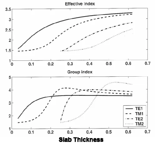
Figure 8. Effective and group index for both polarizations of the first and second order modes of a silicon slab at λ=1.55µm. The slab thickness is given in microns.
As a result, the optical mode would be extended well outside of the silicon film, requiring a very thick cladding on top and bottom of the film, and detrimentally impacting the bend radius of the waveguide. Additionally, since the modulation scheme envisioned required injection of carriers in the silicon, it was desired to have more of the light confined in the silicon. Thus, integration with FD SOI requires additional complexity in the wafers, such as the double stack solution discussed in Chapter 3.
Partially depleted transistor technology
many optical components require high-performance analog and RF circuitry, consideration of this effect must occur during the selection of the CMOS process and will impact the wafer chosen for implementation.
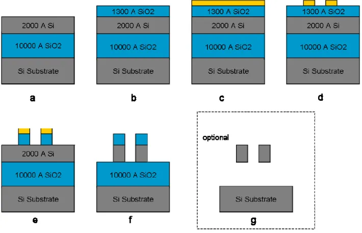
Summary of Technology Platform as of this writing
While this author cannot take sole responsibility for the current state of the technology, it is important to consider the present level of performance of the components described herein, if only for a testament of their potential for commercial success. Much of the original work done during the early stages of this activity could be questioned with regard to the relevance, or the ability, of the technology to scale to the point that the use becomes practical. It is hoped that a brief summary describing the current capabilities will put such concerns at rest.
Overview of the Photonically Enabled CMOS Process
Figure 9. A cross-sectional diagram of key components of Luxtera’s technology implemented monolithically, and sharing the same processing steps
C h a p t e r 2
EXPLORING SILICON PHOTONICS
The work covered in this section spans June 1998 through late 2001, and was performed at Caltech, primarily in the facilities of the Nanofabrication Group. Three key devices constructed during this period will be discussed, a switching polarizer, passive ring resonators, and Erbium clad active ring resonators.
Switching Polarizer
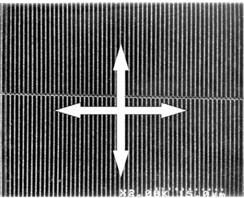
A diagram of a switching polarizer is shown in Figure 10. Collimated light is passed through the plane of the device, which is configured as a transmissive, absorption-based polarizer. Such polarizers are constructed of sub-wavelength conductors, aligned parallel. When light with the electric field polarized parallel to the conductors is incident, electron movement is excited in the conductor, which experiences resistive loss, making the film opaque. When light of the orthogonal polarization, aligned transverse to the conductors is applied, no excitation of the carriers is created, allowing the light to pass through without attenuation.
Basic Device Design
Figure 10. A close-up SEM view of a portion of a silicon membrane patterned to form a polarizer. The cross-bar in the center of the picture was found to be necessary to prevent “stiction” of the beams together, and was repeated every 25µm. The total membrane was 100x100µm. The two orthogonal input polarizations are indicated by the arrows.
For convenience, light of 633nm was chosen as the pump wavelength, and light from an Erbium pump laser of 1.48µm was chosen as the signal wavelength. To be compatible with materials on hand, a silicon film thickness of 200nm was used.
In order to avoid diffractive effects on the signal wavelength, the pitch of the grating must be chosen to be under the free-space wavelength of the light. Thus, a 1µm pitch was chosen. Additionally, it was desired that the cross-section of the grating members be less than the wavelength of light in that material. Using this criteria, a 300nm cross-section was chosen.
Free carrier-effect calculations
Silicon under illumination by 633nm light has an absorption coefficient of 2900cm-1, as can be
seen in Figure 6. In a 220nm thick film, this equates to 6.2% absorption of the incident light. Taking into account reflections at the front and back surfaces of the film results in absorption of just under 3% of the incident light. Furthermore, only 30% of the film surface is remaining after patterning, leaving an absorption factor of 1%. Thus, with a measured incident laser power of 4mW, only 40µW was absorbed in the silicon.
A 633nm photon contains (E=hf) 3.14×10⁻¹⁹ J, meaning that 1.3×10¹⁴ photons/sec were being
absorbed. This power was dissipated in a volume of silicon 0.01mm², by 220nm thick, and only 30% populated, resulting in an e-h pair generation density of 8.5×10²³ e-h pairs/cm3/sec.
The carrier lifetime eventually sets the steady state carrier concentration under illumination, and in these small structures surface recombination was expected to play the dominant role in the carrier lifetime, resulting in a small expected lifetime, postulated to be ~1ns. Under these conditions, the carrier concentration under illumination would be 1014cm-3. This should create
a small modification of the conductivity of the silicon, though not a dramatic effect as will been in the later section concerning free carrier modulation.
Fabrication
An SOI wafer from Silicon Genesis Corporation was acquired. The top silicon film of the wafer was 220nm, and it was separated from the substrate by 400nm of buried oxide. The substrate was 525 microns thick. CVD deposition of 60nm of Si3N4 was performed on both
sides of the wafer by a commercial vendor, which was subsequently segmented into die, each about 0.5cm² via the scribe and break technique. Then, photolithography was performed on the back of die, which was exposed and developed to reveal a square feature centered on the back. The Si3N4 in the exposed area was etched via ECR. After this was performed, the
Figure 11. Fabrication steps involved in construction of a silicon membrane: a) silicon nitride etch mask is deposited on both sides of the wafer and patterned on the bottom. b) anisotropic etch of the silicon wafer using KOH c) etch of the buried oxide using HF d) removal of the nitride mask using boiling phosphoric acid e) application of PMMA mask, e-beam exposure and development and f) plasma stripping of mask
The KOH etch was performed in a solution made from 30% anhydrous KOH pellets and 70% water, by weight. The solution was brought to a boil, and was calibrated to etch 1µm per minute. Due to the 525µm thickness of the wafer, a 9 hour etch process was required. After removal from the KOH solution, the die were placed in boiling phosphoric acid for 5 minutes to remove the silicon nitride.
The resulting die contained a membrane, formed from silicon and silicon dioxide. A 10 sec. submersion in HF, followed by ethanol, removed the remaining silicon dioxide leaving a simple silicon membrane.
PMMA was spun on this film, and e-beam lithography was performed. The PMMA was developed, and the die was etched using a XeF2 process. After the XeF2 was completed, the
die was placed in an O2 plasma for 30 min. to strip the PMMA. The resulting die contained a
suspended structure, as shown in Figure 11.
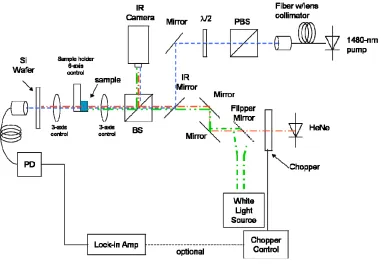
Figure 12. Test setup used to evaluate the performance of the polarizer under the influence of modulation. The chopper provided the modulation signal to the grating, which was then correlated with the modulated 1550nm light via the lock-in amplifier. The white light source was used in conjunction with the camera to image the device for alignment of the IR beam.
Testing
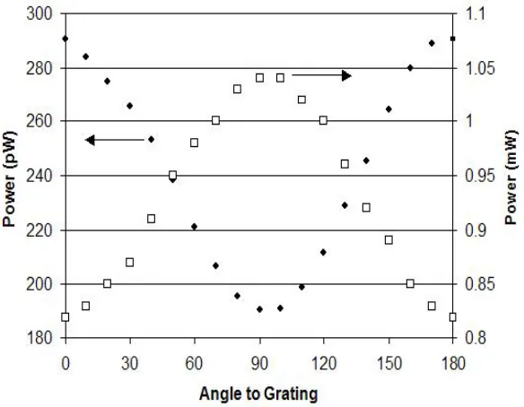
[image:31.612.132.513.182.447.2]Figure 13. Data taken from switching polarizer. The power of the 633nm HeNe is shown on the right axis. Note that the transmitted power reaches a maximum when polarized orthogonal to the gratings, as expected. The left axis shows the OMA of the 1480nm laser, as detected by the lock-in amplifier.
As shown in the DC output, the structure acts as a polarizer, resulting in peak transmission when the light is polarized orthogonal to the grating structure. At this point, the magnitude of the modulation is less, as expected. When the light is aligned with the grating, the transmission drops to a minimum, although the effect of the modulation is greatest at this point. This effect was verified through several repeated measurements of the sample over the course of a week. Due to the faint nature of the output signal, the integration time of the lock-in amplifier, was set up to 100s, resulting in a time-consuming measurement.
Results and discussion
performance of the device was not at levels that were exciting from a practical perspective. Granted, there is substantial room left for improvement of this device. First, the film could be substantially thicker. This would allow greater absorption of the pump light, and thus, a higher carrier generation rate. Additionally, the thicker film would increase the carrier lifetime, creating a higher carrier density under illumination. Also, surface treatments, such thermal oxidation or forming gas annealing could be used to increase carrier lifetime.
A preferred way to produce the same effect is to use electrical modulation instead of optical pumping. It is hypothesized that an increased effect would be seen in this situation, were carrier concentrations can be modified at substantially higher levels than those used achieved in this work. For example, MOS capacitor structure, formed in the shape of a grating could be used to accumulate charge underneath the gate, rapidly forming a conductive structure suitable for absorption of a single polarization. Additionally, it would be possible to form an interdigitated p-n diode, which would have the conductivity of the film modified by forward or reverse-biasing. At levels of adequate reverse bias, the film would contain no conductive structure what-so-ever, which would be an improvement over the MOS capacitor approach, where the gate structures would serve as a polarizer independent of the applied voltage.
Though this device served as proof-of-principle, due to the poor performance and lack of an exciting real-world application, it was decided to not conduct further experiments on this device, and to move on to waveguide structures, where the interaction length of the light and the material could be made substantially longer.
Ring resonator fabrication
Figure 14. a) directional coupler optical motion transducer device concept. b) disk resonator version
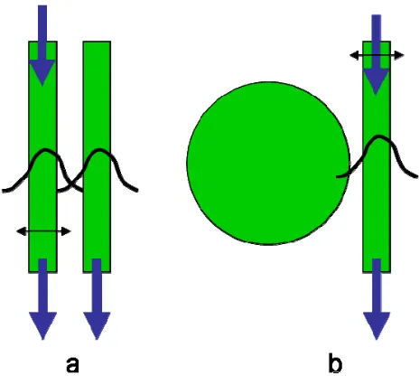
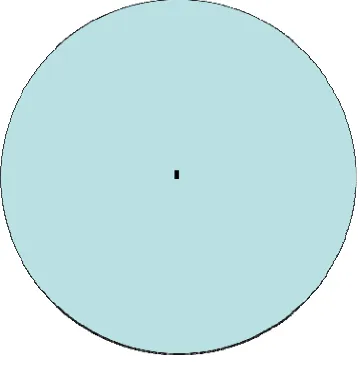
However, a large number of technical challenges remained to be overcome before such an experiment could be realized. First, these devices containing submicron features must be fabricated, and secondly, light must be coupled into these devices with enough efficiency to allow the measurement to be made. Neither of these tasks is trivial. Figure 15 illustrates the mechanical relationship, to scale, between the core of single mode fiber and the waveguides envisioned for this experiment, which must be minimal in cross-section. As one can see, the coupling efficiency between the two waveguides is necessarily extremely small. Based on cross-sectional area ratios, a typical estimation technique, -27dB of light would be lost, both upon entering and leaving the waveguide. Such losses would pose a dramatic problem inside a cryogenic environment, as the lost power would become heat as the light was absorbed on the chamber walls.
Figure 15. Drawing, approximately to scale, of the core of a single mode fiber (circle) compared to a 200x400nm waveguide (rectangle). This illustrates the problem associated with butt-coupling approaches often used to couple fiber with to larger waveguides.
patterning and development of the PMMA, a RIE etch is performed to pattern the oxide. At this point the PMMA is removed and the part is transferred to the ECR etching chamber where the silicon etch is performed. After this step, a wet oxide etch is used to suspend the part, followed by a critical-point drying process to avoid deformation of the part experienced during evaporation of the solvents.
The first attempts at device fabrication focused entirely on the suspended portion of a directional coupler device. This device was chosen for the complexity of processing steps required in construction, as it was expected to be a worst case example, requiring submicron resolution over a long distance, and successful suspension of two structures within close proximity to each other.
top view
[image:37.612.244.405.199.341.2]perspective view
Figure 17. Top and perspective views of a pair of silicon nano-mechanical beams fabricated in close proximity and suspended. Each beam measured 400x200nm, and was 10µm long.
performed in a 100x100µm square with adequate resolution to resolve the desired devices. Thus, an approach was devised where traditional photolithography would first be employed to fabricate large, multimode waveguides that would extend to the perimeter of a die, and which would connect to an unpatterned region of silicon in the center of the die. This pattern is shown in Figure 18. The top silicon film of the SOI wafer would be etched away in all regions except the waveguides, alignment marks, and the center pad. In order to allow for alignment for the ebeam lithography step, the central pad was chosen to be 40µm square, and the corners of the SEM field of view would be used for alignment.
In order to test this approach, a simple 3-way splitter was first designed. This splitter would allow verification of a 4 port device, such as a directional coupler or MZI constructed from 2 directional couplers.
Using the alignment marks left from the first processing step, the ebeam pattern was written on the central pad, which was etched to form the completed devices. Several resulting devices are shown in Figure 19. Despite numerous attempts at this type of device construction, alignment between the original waveguides and the final waveguides could not be achieved with sufficient accuracy.
a b c
Figure 19. Three separate attempts to align a 3 way splitter to the structure illustrated in Figure 18. In each case, note the alignment between the optically defined and e-beam lithography defined waveguides. In (a), the dark squares are charging of the oxide associated with SEM inspection of the misalignment.
Thus, this technique was abandoned for a second approach that did not require a two-step process. Instead, the structures would be fabricated to contain a 90° bend in the waveguides, and would be fabricated in a small area in the center of a die. The die would subsequently be cleaved along two axes, exposing the input and output waveguides to the edge of the die. At this point, the die would be placed in a mechanical alignment stage, and polished fibers, or high numerical aperture optics, could be brought to each edge of the die for coupling.
a b c
Figure 20. Three devices fabricated with the intention of suspending the waveguides in order to optically measure the mechanical vibration. They are: a) a directional coupler, b) a Mach-Zehnder Interferometer, and c) a disk resonator.
Figure 21. Cleaved endface of a SOI waveguide written with a stitching stage ebeam lithography system. Note the stage stitching error seen on the waveguide sidewalls.
Results and Discussion
This concludes the attempts to use SOI waveguide devices for mechanical transducers. In summary, this effort successfully yielded device fabrication processes, and a number of high-quality nanofabricated devices, although measurement was not practical. This highlighted a fundamental issue with the development and construction of high-index contrast photonics – it was essential to develop a technique to get light on and off the chip before the technology could be practical, even for academic purposes. Rather than embark on an effort to build a hero device by many repeated attempts, it was decided to solve the problem by generating light on the die.
Erbium doped light sources
300x300nm optical waveguide, with air cladding and glass cladding. The mode is extended into the glass as the index contrast is reduced, resulting in a confinement factor of 50% in the glass.
This realization lead to the concept of an erbium-doped glass cladding, which could be pumped surface normal in addtition to resonant pumping. In either case, amplification occurs through overlap with the evanescent field and the excited Erbium. This concept is shown in Figure 23.
a b
Figure 23. a) Ring device fabricated for deposition of Erbium doped glass b) after deposition of glass. Device to be pumped from above.
Fabrication
structures. This hardmask can not be removed without undercutting the oxide underneath the waveguides. Since the field concentration is highest close to the waveguide, this region required deposition of Erbium material, so a technique must be devised that did not require the use of a hardmask. The approach chosen was to construct a XeF2 etching system, which was known to have a low etching rate in PMMA as compared to silicon.
A CAIBE system was modified with a XeF2 chamber, which consisted of a stainless steel
chamber clad in heating tape. XeF2 tablets were introduced to the chamber, though under heat and vacuum, they were converted into gas and introduced to the CAIBE chamber via a mass flow controller, essentially taking the place of the Chlorine typically found in such systems. After the etching step was performed, the PMMA could be removed in a combination of solvents and oxygen plasma stripping.
At this point, an oxide cladding was deposited by spin-on-glass, which contained Erbium in varying concentrations. Additional samples were constructed by reactive sputter deposition of silicon dioxide, followed by implantation of Erbium. Pictures of two fabricated device are shown in Figure 24.
Defect used for free-space coupling Defect used for free-space coupling
Figure 24. Photographs of a high quality disk resonator and a low quality ring resonator fabricated for Erbium deposition. Normally, sample a) would have been scrapped, but the defect structure allowed wafer normal test to occur.
Testing
Figure 25. Spectrum of Erbium implanted silicon dioxide deposited on top of a silicon waveguide, and pumped from above.
modes found in photonic crystals. However, the accidental fabrication of a device with a clear defect in the ring raised the question about coupling into the resonator through use of a scattering site. This approach was successful, and did not require alignment to the output waveguide. Figure 26 shows the resonant spectrum observed from this measurement, both prior to and after erbium doped glass deposition. Note that the defect scattering site present in the ring adversely impacts the Q of the ring, and as such, the measured Q is substantially below the required value of 20,000.
Figure 26. Top: Resonance spectrum of a the ring without Erbium doped glass deposited. Bottom: After deposition. Note reduction in Q and reduction in extinction ratio of the ring after Erbium was deposited, indicating enhanced absorption.
At this point, a survey of all known coupling techniques was undertaken to develop a better approach for coupling into the small waveguides required desired for high-index contrast silicon waveguides.
Table 1. Summary of the known techniques for coupling into high-index waveguides, arranged in order of popularity.
great success. Of the remaining two, the prism coupler showed little promise for eventual integration into CMOS. The final option, the grating coupler, was known to be inefficient, narrowband, and extremely difficult to design and fabricate. However, the potential for surface normal testing, which eliminates the need for edge preparation, was a substantially appealing, leading to the decision to explore this device further.
Grating coupler simulations and theory
The grating coupler was an extension of the concept used in the prior section for measurement of the ring resonator through a scattering site. However, careful construction of an array of scattering sites, similar to a phased-array antenna, could effectively provide “antenna gain,” allowing a higher coupling efficiency to be achieved [19]. This is the basic principle behind grating coupler design, and while difficult, it has be demonstrated that this technique has the potential to be over 90% efficient over several THz of optical bandwidth.
[image:47.612.239.410.483.591.2]A grating coupler is quite simply an array of scattering sites placed in sequence down a waveguide, as shown in Figure 27. For an optical mode traveling in the waveguide, each scattering site has a scattering efficiency, radiation profile, and a phase delay for transmitted light. Knowledge of these parameters allows calculation of the emitted optical field, which can then be analyzed for mode matching with the external optics, such as an optical fiber.
Figure 28. k-space diagram for light incident on an air glass interface from within the glass. The dashed line indicates the transverse wavenumber, which must be preserved in all allowed modes.
For light of a given wavelength, λ0, in a material with a bulk refractive index of n, the propagation vector will have a total magnitude of
where 0 2 λ π = k
This can be represented as circle in 2D k-space, requiring
2 2 2 y x k k
k = +
Figure 28 shows the resulting diagram containing circles representing the allowed propagation vectors for both air and glass. The origin is considered to be at the physical interface, and as such, dashed lines are used to represent a propagation vector that is not allowed, due to the absence of the appropriate material. Thus, for propagation in air, is shown by the solid line to only be allowed in the lower half of k-space, and propagation in glass is shown by the solid line to only by allowed in the upper half of k-space, in effect representing the non-reciprocal space representation of the interface.
Thus, light scattered from the interface is only allowed to propagate with wavenumbers associated with the solid circles. However, the dashed lines are essential in order to represent the original incident light as a vector relative to the origin of k-space. Thus, in each of the following diagrams, the incident light is shown on the dashed circle, and the scattered light is shown on the solid circles.
For any dielectric interface, it can easily be proven that the transverse wavenumber must be conserved across the interface. Thus, the transverse wavenumber of the incident light is represented by the vertical dashed line. This line intercepts solid (allowed) portions of the two circles, indicating that light is allowed to travel in both directions, indicating the wavenumbers of both the transmitted and reflected modes from this interface. Note that this is nothing more than a geometric representation of Snell’s Law, and the angles of the reflected and transmitted light agree with Snell’s Formula, which in this material system can be written as
Figure 29. k-space representation of a transmission grating formed on a air/glass interface with the light incident from within the glass. Dashed lines represent the transverse wavenumbers of the supported diffractive orders.
a
π
2 = Λ
[image:51.612.161.487.387.609.2]and will serve to modify the transverse wavenumber in discrete steps with this periodicity. Each of these discrete steps is typically referred to as a diffractive order of the grating. Figure 29 shows the allowed diffractive orders, -3 to +1 of this grating. Note that there are a different number of reflected and transmitted orders, with the sign of the order being defined by the chosen coordinates of k-space. In this case, 8 diffracted orders are allowed, although this number will shrink as the physical dimension of the grating period is reduced. This results in a larger spacing between modes. Note that with a sufficiently small grating pitch, it’s possible to have a single diffracted order, in addition to the reflected and transmitted modes.
Figure 30 extends this k-space concept to a waveguide. In this case, the waveguide core is silicon, and the cladding is silicon dioxide, resulting in circles with a radius of nsik0 = 3.5k0 and
ngk0 = 1.5k0 respectively.
waveguide is commonly known as what we’re referring to here as the vertical wavenumber.)
Of course, the oxide cladding is present both on the top and bottom of the waveguide, and as such, light is allowed to travel in any direction in the cladding.
[image:52.612.157.488.414.635.2]In 3D, each of the circles shown here becomes a sphere, and the slab waveguide mode becomes two parallel circles perpendicular to the page, and intersecting the sphere at the points shown.
Figure 31 shows a possible outcome when the waveguide is combined with a grating. In this case, known as forward coupling, the incident light is coming from above at a steep angle to the grating. Note that the light can momentarily enter the silicon and travel on through the bottom cladding. Also, a reflected mode is allowed in the upper cladding. If a grating was not present, there would be no other effect. However, the grating in this case is chosen to have a pitch
( )
θ β −ngk0sin =Λ
[image:53.612.150.492.376.610.2]creating phase matching with a waveguide mode traveling in the positive direction. Note that while a diffracted order is present in the negative direction, it is not vertically resonant with the waveguide film, and as such, is not allowed to propagate. In this case, the light can be efficiently coupled to a single waveguide mode traveling in one direction. However, the transmitted and reflected modes still exist and will create waveguide coupling inefficiency.
k-space representation would reflect exactly this condition. However, due to the finite size of the gratings, the k-space representation of the allowed diffracted orders is broadened. However, due to the absence of any other allowed modes, this broadened k-space diffraction can still be highly efficient.
As the radius of the circles change with the frequency of the light, the grating momentum remains constant. In the forward coupling case, the reduced rate of transverse wavenumber walkoff will slightly extend the range over which the grating operates, and in the reverse coupling case, this will slightly reduce the range of operation. Also, note that the closer the rate at which the transverse wavenumber matches the change in beta, the greater the wavelength range over which the grating couples light into the slab.
For the forward coupled case, it’s possible to match these numbers over a limited frequency range, or at least to design in such a manner that the difference is minimized. This technique allows design of grating couplers that are more broadband than a standard coupler. However, such a design suffers from the requirement to use a high incident angle, which is not always practical.
structure and does not consider the case of interfacing to a real 3D mode. These issues are addressed in a complete design methodology.
Grating Coupler Design Methodology
The baseline case indicated by the k-space argument is a uniform, periodic grating of a chosen periodicity. However, this model needs to be modified in a number of ways before design of an efficient grating coupler can be achieved. For purposes of this description, a single mode fiber will be considered as the desired optical system to interface with.
[image:55.612.270.379.371.534.2]While in the previous section, the system was considered from the point of view of light incident on the grating from an external source. In the following discussion, the grating will be considered from the point of view of light in the slab waveguide, which will impinge on the grating and be scattered into the cladding regions. The reciprocal nature of the grating permits design from either perspective, and will create identical results.
Figure 33. Exponential radiation profile from a uniform grating.
Gaussian Emission Profile
Figure 34. Illustration of relationship between power decay in the waveguide (dashed) and ideal grate scattering strength.
Grate Radiation Pattern
Figure 35. Radiation power scattered from a single “grate” deposited on a waveguide. Vectors indicate poynting flux through points along a box surrounding the grate. Note fraction of power scattered up.
Scattering Strength
In order to emit light within the small distance required by the cross-section of a single mode fiber, it’s important that each individual grating be fairly strong, on the order of 10%. A typical transmission range is shown in Figure 36.
either the forward or backward coupling case. A picture of the resulting device is shown in Figure 37.
Figure 37. A SEM photograph of a grating coupler formed from polysilicon grates deposited on a hyperbolically flared silicon waveguide. The footprint of the grating represents a 10µm optical fiber mode. The output waveguide is 200x400nm.
Variable Grate Phase Delay
semi-periodic, and that the ramp in periodicity is not necessarily a linear function of the grate dimensions.
Vertical Film Stack
Finally, it’s possible to cancel out the mode directed at the substrate by reflecting it back towards the surface and using this light to cancel the reflected mode. As illustrated in Figure 38, the phase of this reflected light must be carefully considered, or destructive interference is created. However, when constructive interference is achieved, the efficiency of the device is greatly improved.
Figure 38. a) Destructive interference created by inappropriate choice of oxide thickness. b) Correct oxide thickness creates more efficient coupler. Any reflector will suffice, although DBR is shown.
Grating Library
reflected component of light is simply the mirror image of the emission from the reflected light. After all contributions are summed, an emission profile for the light traveling up and down from the grating is constructed. The grating design can be optimized by taking the overlap integral of these modes with that of a fiber mode. The goal at this point in the design is to optimize the mode to more perfectly match a fiber mode for both the up and down traveling light.
Table 2. Simulated impact of substrate reflectivity on peak efficiency of an example grating coupler. Wafer factor refers to the number of reflective layers in the substrate. The negative number indicates a perfectly out of phase condition.
developed over time from the simple process required to demonstrate grating couplers and waveguides to a complete integration of the technology with an existing CMOS process. Information contained in this thesis will cover the proof of principle work only, and will not consider the details of reliability, yield, and process stabilization required for product development.
Grating Coupler Realization
Figure 39. Simulation and experimental results from the first grating coupler design.
Measurement technique
[image:63.612.206.443.288.421.2]Grating couplers are measured by constructing a short loop of waveguide connecting two identical grating couplers. A fiber array with the correct spacing to match the gratings is brought into close vicinity of the grating loop, and the transmission is optimized. After optimization, a wavelength scan is taken using a tunable laser. The measured loss experienced traversing two grating couplers is then halved to indicate the loss of a single grating coupler. Note that due to the short length of waveguide, ~150µm, waveguide loss is negligible.
Figure 40. A test loop consisting of two identical grating couplers, connected by a short waveguide. Spacing is 127µm.
Wafer-scale Test
Figure 41. Photograph of wafer probe capability showing RF and low frequency electrical probes from the top and sides respectively. Optical fiber probe enters from the bottom of the picture. Fibers exit normally from the surface of the wafer and curve out of the picture on the left hand side. The wafer is the green surface below the probes.
This capability allows wafer mapping of key optical parameters, such as grating coupler efficiency shown in Figure 42. This allows correlation with processing parameters and other sources of variability to be studied, so that problems can be diagnosed and better understood. For example, the ring pattern shown in this wafer plot indicates that the peak efficiency is experiencing an impact from a film deposition know to have this signature.
[image:64.612.232.417.508.658.2]Ring resonators
Ring resonators are very interesting components for use as filters and modulators. Their simplicity, combined with their small size makes them a compelling option for implementation in a system architecture based entirely on rings. Furthermore, use of rings for measurement of waveguide loss and effective index makes them useful diagnostic tools to be employed in a small area within a wafer.
Figure 43. Ring resonator configured as an add/drop filter. The ring diameter is 5µm.
Ring Resonators as Filters
systems today, 4THz is the width of the optical C-band, which contains 40 channels, and 195THz is the frequency of 1550nm light. Note that in order to convert to ring radius, the optical pathlength needs to be divided by 2πne, which is approximately 20. Thus, to have a
[image:66.612.196.455.374.575.2]single ring capable of isolating an individual wavelength over the C-band, the radius of that ring must be less than ~3.75µm!
Figure 44. Effective optical pathlength vs. cavity FSR, and the required cavity length for several interesting frequency spans.
Single Pole Filter Design
of rings, and avoids the crosstalk associated with the control algorithms for multiple rings. Figure 45 illustrates the case when a ring with a Q of 10,000 is used as a single pole filter for channels with 100GHz spacing. The crosstalk between adjacent channels is -20dB in this configuration, which is acceptable for a data link, assuming the link is capable of handling the associated power penalty. To minimize distortion, it’s desired to have the Q of a ring used as a filter as low as possible, while trading off the impacts on the link penalty due to adjacent channel crosstalk. This allows some room for misalignment in addition to minimizing the distortion link penalty.
Figure 45. Filter shape of ring with Q=10,000. Adjacent channels plotted with dashed lines, demonstrating -20dB crosstalk with each adjacent channel.
For most applications, a total crosstalk of about -15dB is an acceptable value to ensure minimal impact on the link performance.
Figure 46. Calculation of power penalty as a function of bandwidth and misalignment for a ring resonator.
Figure 47. Data taken from the drop and transmission ports of a ring filter. Vertical axis in dB.
This sets the motivation for a 15 micron radius ring with low insertion loss, and a Q of about 10,000. Figure 47 shows the test results for a ring resonator configured for multiplexing. This particular device was designed for 10Gb data, and with a FSR capable of handling 4 channels, spaced 100GHz. The Q for the device was 10,900, higher than the target of 10,000. This allows a passband of 18GHz, which will slightly clip the double sideband 10Gb data. In order to increase the passband, the device should be more strongly coupled to the input and output waveguides. The FSR of the ring was 450GHz, which is more than adequate for a 4-channel multiplexer. Note that the loss on the dropped wavelength was quite small, <0.5dB. The 4dB background loss results from fiber coupling on and off the chip. These numbers represent fiber-to-fiber insertion loss of a packaged device.
Figure 48. Transmission measurement of a 2µm radius ring, creating a 45nm (56THz) FSR. Inset shows measured ring and waveguide.
Rings as Diagnostic Structures
Figure 49. Spectrum of a corrugated ring showing critical coupling at the resonance order associated with the corrugation period. Upper inset shows coupling region of ring structure. Lower inset shows close up view of deep resonance.
Figure 49 shows measurement results from one such ring. Note that the resonance of the coupled mode is split, as predicted by theory. This allows determination of the precise mode number observed in the ring. With this information, the remainder of the resonances can be used to extract the effective index, and consequently the group index as well. The excellent correlation between the ring measurements and measurements taken from the reflection of straight corrugated waveguide are shown in Figure 50.
Figure 50. Corrugated waveguide measurements (red dots) plotted with continuous curves extracted from ring measurements.
Rings as Modulators
Figure 51. Time constant of a cavity as a function of Q for 1.55µm light.
There is a fundamental tradeoff between Q and the amount of index modulation achievable. Fundamentally, the fraction of the resonant frequency that can be moved is exactly proportional to the fraction that the wavelength of the light in the waveguide can be changed. Since the wavelength of light in the waveguide is determined by the effective index, ne, it’s
correct to say
f f n
n
e e =∂ ∂