N A N O E X P R E S S
Open Access
Nearly full-dense and fine-grained AZO:Y
ceramics sintered from the corresponding
nanoparticles
Ye Yang
1, Pinjun Lan
1, Muqin Wang
1, Tiefeng Wei
1, Ruiqin Tan
2and Weijie Song
1*Abstract
Aluminum-doped zinc oxide ceramics with yttria doping (AZO:Y) ranging from 0 to 0.2 wt.% were fabricated by pressureless sintering yttria-modified nanoparticles in air at 1,300°C. Scanning electron microscopy,
energy-dispersive X-ray spectroscopy, X-ray diffraction analysis, a physical property measurement system, and a densimeter were employed to characterize the precursor nanoparticles and the sintered AZO ceramics. It was shown that a small amount of yttria doping can remarkably retard the growth of the as-received precursor nanoparticles, further improve the microstructure, refine the grain size, and enhance the density for the sintered ceramic. Increasing the yttria doping to 0.2 wt.%, the AZO:Y nanoparticles synthetized by a coprecipitation process have a nearly sphere-shaped morphology and a mean particle diameter of 15.1 nm. Using the same amount of yttria, a fully dense AZO ceramic (99.98% of theoretical density) with a grain size of 2.2μm and a bulk resistivity of 4.6 × 10⁻³Ωcm can be achieved. This kind of AZO:Y ceramic has a potential to be used as a high-quality sputtering target to deposit ZnO-based transparent conductive films with better optical and electrical properties.
Keywords:AZO:Y Ceramic, Nanoparticles, Coprecipitation, Sintering, Finer grain, Nearly full density PACS:61, 61.66.Fn, 61.72.uj
Background
Transparent conductive oxides (TCO) as transparent elec-trodes have been widely used in thin-film solar cells and flat panel display devices [1,2]. The commonly applied TCO materials are In2O3:Sn (ITO), SnO2:F (FTO), and
ZnO:Al (AZO) [1,2]. AZO has attracted much interest as a potential substitute for ITO due to the abundance of its constituent elements in nature, relatively low deposition temperature, and stability in hydrogen plasma [2,3].
The magnetron-sputtering ceramic target is one of the most widely used methods for AZO film deposition [3]. In the sputtering system, the target plays a major role in achieving high-quality films [4-7]. Generally, the target for sputtering TCO films should have a high density, finer grain size, and better conductance [7-11], which will be helpful for avoiding the formation of nodules to
prolong the target lifetime [7,8], increasing the depos-ition rate and film uniformity [9] and meeting the re-quirement of direct current (DC) sputtering. The attempts to enhance the density of the AZO ceramic get become a crucial issue for both researchers and tar-get manufacturers [7,8,12-14]. Sun et al. [12] fabricated an ultrahigh-density AZO sintered body (>99.7% theor-etical density) after pressureless sintering at 1,400°C by adjusting the mass fraction of polyacrylic acid when slip casting a mixture slurry of commercial ZnO and 2 wt.% Al2O3powders. Hwang et al.[13] found that the
prelim-inary heat treatment under external pressure increased the density and uniformity after a final sintering. The maximum density value of 2 wt.% Al-doped ZnO sin-tered at 1,350°C was about 5.52 g/cm3 (approximately 98.9% of the theoretical density). Recently, Zhang et al. [14] used a two-step sintering process to obtain the AZO ceramic with a relative density of more than 99% by sintering the 30-nm sol–gel-synthesized AZO nano-particles at the second-step sintering temperature of 1,000°C for 12 h. To our best knowledge, the nearly
full-* Correspondence:[email protected]
1Ningbo Institute of Material Technology and Engineering, Chinese Academy
of Science, No. 519, Zhuangshi Road, Zhenhai District, Ningbo 315201, People’s Republic of China
Full list of author information is available at the end of the article
dense (namely, exceeding 99.9% of the theoretical density) AZO ceramic has rarely been reported and still kept a challenge as before, especially by a simple and low-cost pressureless sintering at a relatively low temperature.
Few studies have also shown that a small amount of a rare earth element such as yttrium introduced into a ZnO matrix can obviously improve the proper-ties of both ZnO films and the corresponding ceramic sputtering targets [15-18]. For example, Han et al. [16] have utilized an electrochemical deposition method to obtain a 3.7 at% yttrium-doping ZnO film with a resistivity of as low as 6.3 × 10⁻⁵Ω cm after post-deposition annealing in nitrogen at 300°C. GfE Co. (Nuremberg, Germany) has produced a novel aluminum-doped zinc oxide ceramic with yttria dop-ing (AZO:Y) target containdop-ing a small amount of Y2O3 besides Al2O3, which can be stably sputtered by
pulsed DC sputtering technology due to the higher conductivity [17,18]. Using this kind of target, Tsai et al. [19] found that the thin AZO:Y film deposited at 300°C had the lowest resistivity of 3.6 × 10⁻⁴Ωcm, the highest mobility of 30.7 cm2 V−1s−1, and the highest carrier concentration of 5.6 × 1020cm−3.
However, the above mentioned research results mainly focused on the properties of AZO:Y films; the detailed investigation on the influence of Y doping on the mir-crostructure and densification of the AZO ceramic tar-get itself is lacking. In this work, we attempted to fabricate highly dense AZO:Y ceramics by pressureless sintering by a coprecipitation process using Y and Al co-doped ZnO nanoparticles as raw materials, and the microstructure and densification of AZO:Y ceramic were investigated.
Methods
Synthesis of AZO:Y nanoparticles
Y-doped AZO (AZO:Y) nanoparticles were synthesized by a coprecipitation process, using an AR grade of zinc nitrate, aluminum nitrate, yttrium nitrate, and ammo-nium acid carbonate as starting materials (all purchased from Sinopharm Group Co. Ltd., Shanghai, China). A 1 M distilled water solution of Zn(NO3)26H2O, Al
(NO3)39H2O, and Y(NO3)26H2O, whose amounts
were determined by Al2O3/[ZnO + Al2O3] = 2 wt.%
and Y2O3/[ZnO + Al2O3] = 0, 0.1, 0.15, and 0.2 wt.%
(the corresponding samples being named AZO:Y0,
AZO:Y0.1, AZO:Y0.15, and AZO:Y0.2), respectively,
were added to 2 M NH4HCO3 solution drop by drop
at a constant temperature of 30°C with stirring to produce a mass white precipitate. After aging for 24 h, the precipitate was filtrated and washed several times, followed by drying for 12 h in an oven at 100°C. Then, the precipitate was calcined at 600°C for 2 h to form AZO:Y nanoparticles.
Sintering of AZO:Y ceramics
The as-received AZO:Y nanoparticles were first granulated by spray drying to form larger sphere aggregations with a diameter of approximately 10μm and then were pressed by uniaxial pressing (50 MPa, 3 min) in a stainless steel die with a diameter of 8 cm. The green bodies were subse-quently pressed by cold isostatic pressing (250 MPa, 5 min) and sintered in air for 8 h at 1,300°C in an electric furnace. In order to clearly observe the microstructure and conveni-ently measure the conductivity, the sintered specimens were ground and polished with a 1-μm corundum slurry and then thermally etched at 900°C for 20 min.
Characterization
The phases of the AZO:Y nanoparticles and sintered specimens were identified by X-ray diffraction analysis (XRD, D8 Advance, Bruker AXS GmbH, Karlsruhe, Germany) with CuKα radiation (λ= 1.5406 Å) operated at 40 kV and 40 mA and a scanning step of 0.02°/s. The morphology, microstructure, and composition analyses of the AZO:Y nanoparticles and the sintered bodies were performed using a scanning electron microscopy(SEM)/ energy-dispersive X-ray analysis (EDAX) system (S-4800, Hitachi Ltd., Tokyo, Japan). The average particle/grain size of the as-calcined nanoparticle or sintered ceramic specimen was estimated from a minimum of 100 parti-cles/grains obtained from the SEM images by the linear intercept method proposed by Mendelson. The densities of the sintered specimens were determined by Archime-des’s method with a densitometer (MH-600, MatsuHaku Electronic Co., Ltd., Taichung, Taiwan). The bulk resis-tivities were measured by a physical property measure-ment system (PPMS; Model-9, Quantum Design Inc., San Diego, CA, USA) at room temperature.
Results and discussion
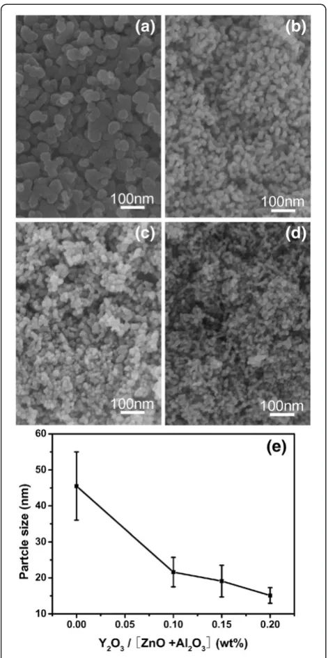
The SEM images of the unmodified (Figure 1a) and dif-ferent amounts of yttria-modified AZO (Figure 1b,c,d) nanoparticles after calcination at 600°C for 2 h as well as the plot (Figure 1e) of particle sizes estimated from the SEM images as a function of yttria content are shown. All nanoparticle samples exhibit a nearly spherical morphology, and the average particle sizes are 45.5, 21.6, 19.1, and 15.1 nm for the AZO:Y0, AZO:Y0.1, AZO:Y0.15,
and AZO:Y0.2samples, respectively, which show a trend
of size decrease with increasing Y2O3contents. The
re-sult of the SEM images suggests that a small amount of Y2O3addition can remarkably retard the growth of AZO
nanoparticles during calcination. In order to explore the phase of AZO:Y nanoparticles after calcination, a 0.2 wt.% Y2O3-doping nanoparticle sample was used to carry out
the XRD analysis, as shown in Figure 2. It can be seen that all diffraction peaks are only labeled to the wurtzite ZnO structure (JCPDS card no. 036–1451) without any
Yanget al. Nanoscale Research Letters2012,7:481 Page 2 of 6
secondary phase diffraction peaks from Al2O3and Y2O3or
their compound. According to the energy-dispersive X-ray spectroscopy (EDS) analyses of AZO:Y0.2 nanoparticles
shown in Figure 3, Al species are found, while the trace of Y species cannot be detected due to its trivial content to the EDS detection. It can be summarized that the role of yttria doping in the calcined AZO nanoparticles is to de-crease the particle size.
The AZO:Y ceramic was fabricated by pressureless sin-tering the calcined AZO:Y nanoparticles at 1,300°C in air. Figure 4 shows the XRD patterns of the sintered spe-cimens at 1,300°C. For all sintered spespe-cimens, except for the main diffraction peaks corresponding to the hex-agonal wurtzite ZnO structure, other small peaks are assigned to the ZnAl2O4 phase. Similarly, the phase
related to the yttrium dopant cannot be observed. Be-cause the ionic radius of yttrium (approximately 0.90 Å) is larger than that of zinc (approximately 0.74 Å), yttrium is hardly doped into the ZnO lattice. Almost all yttrium will react with Al2O3to form an Al2Y4O9phase,
as described in the patent [18] and the literature [20]. In addition, we also use EDS to detect a tiny area with Y ag-gregation around the grain boundary and further verify that the atom ratio of Y to Al is 2.2, which is close to the stoichiometric ratio of the Al2Y4O9phase (not shown in
this paper). Considering the fact that the solubility of the Al element in ZnO is about 0.9 at% as determined by Zhang [21] and that excess Al2O3 totally reacts with
both ZnO and Y2O3 to transform into ZnAl2O4 and
Al2Y4O9, respectively, the final composition of the
sin-tered ceramic can be approximatively expressed as 97.4 wt.% ZnO:Al + (2.6 to 2.5) wt.% ZnAl2O4+ (0 to 0.2)
wt.% Al2Y4O9with varied Y2O3doping . Taking the
the-oretical density (TD) value of ZnO:Al, ZnAl2O4, and
Al2Y4O9as 5.610 g/cm3, 4.640 g/cm3, and 4.520 g/cm3,
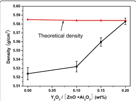
the reasonable TDs of the final sintered AZO ceramics can be deduced to be 5.585 g/cm3for the yttria-undoped ceramic and approximately 5.583 g/cm3 for the yttria-modified ceramics using a weighted average calculation. The measured densities and the TDs as a function of Y2O3
[image:3.595.56.292.87.561.2]concentrations are plotted in Figure 5. Increasing the
Figure 1SEM images and the calculated particle sizes.Images of AZOY nanoparticles calcined at 600 °C for 2 h: (a) AZO:Y0, (b)
AZO:Y0.1, (c) AZO:Y0.15, and (d) AZO:Y0.2. (e) The plot of the particle
sizes calculated from (atod) SEM images as a function of Y2O3
content.
Figure 2X-ray diffraction pattern of nanoparticles.X-ray diffraction patterns of (a) calcined AZO:Y0.2nanoparticles and (b)
[image:3.595.306.538.88.263.2]Y2O3 content, the density of the sintered specimen
increased from 5.524 g/cm3 (98.90% of TD) without any Y2O3 doping to the highest one of 5.583 g/cm3 (99.98%
of TD) with a Y2O3 content of 0.2 wt.%. So, the small
amount of Y2O3 addition can obviously enhance the
density to be close to the theoretical density. Fur-thermore, our research also reveals that the Y2O3
content beyond 0.2 wt.% will severely deteriorate the density of the AZO ceramic (not shown here). A doping content of 0.2 wt.% Y2O3should be the most
optimal one.
In order to understand the effect of Y2O3modification
on the microstructure of the sintered AZO ceramics, SEM was employed to observe the polished sample sur-face, as shown in Figure 6a,b,c,d. For the AZO:Y0
sam-ple, one can observe that the grain is not uniform with an average size of about 5.7 μm, and some small white particles with a size of approximately 0.5 μm uniformly disperse in an inner grain and/or grain boundary. These smaller white particles are deemed to be the secondary-phase ZnAl2O4, as described by Han et al. [22] and also
determined by EDS analysis as shown in Figure 6e,f,
where the abundant Al element in the white particles is much higher than that in the AZO:Y grain. In addition, there are some small cavities and microstructural defects in the sintered body. However, with increasing Y2O3
content (shown in Figure 6b,c,d), the grain size decreases to 2.0, 2.4, and 2.2 μm for AZO:Y0.1, AZO:
Y0.15, and AZO:Y0.2, respectively, where the grains
be-come more uniform than those in the AZO:Y0 sample.
Meanwhile, the small cavities and microstructural defects almost disappear with the increase of the Y2O3
content, implying an increase in density. This result is also in accordance with the measured density shown in Figure 5. So, the observation on the microstructure demonstrates that the addition of a small amount of Y2O3may also play a key role in increasing the density,
refining the grain, and improving the microstructure uniformity. The reason for achieving a highly dense AZO ceramic with a fine grain can be ascribed to the following two factors: The first may be due to the use of finer AZO:Y raw nanoparticles, which possess a much higher sintering activity. Due to the smallest particle size, AZO:Y0.2 nanoparticles can be easily sintered to
[image:4.595.61.540.89.207.2]bemore dense at a relatively low temperature. The
[image:4.595.57.290.516.693.2]Figure 3EDS pattern of nanoparticles.EDS pattern of AZO:Y0.2nanoparticles.
Figure 4X-ray diffraction patterns of sintered ceramics.X-ray diffraction patterns of the 0, 0.1, 0.15, and 0.2 wt.% Y2O3-doped AZO
[image:4.595.305.538.522.695.2]ceramics sintered at 1,300°C.
Figure 5The measured densities and the theoretical densities. The measured densities and the TDs as a function of Y2O3
concentrations.
Yanget al. Nanoscale Research Letters2012,7:481 Page 4 of 6
second may be due to the existence of the secondary-phase particles in the grain boundary. Be-sides ZnAl2O4 particles, the introduction of Al2Y4O9
into the grain boundary by Y2O3 doping can further
refine the grain size by inhibiting the grain growth by pinning or dragging the migration of grain boundaries [22].
Except for a high density and fine grain, a low resistiv-ity of the AZO ceramic target will meet the requirement of DC sputtering with a high deposition rate [5]. To study the effect of yttria addition on the bulk resistivity of the AZO ceramic, PPMS was used to measure the re-sistivity; the results are listed in Table 1. It can be found that the Y2O3 addition in the AZO matrix does not
change the resistivity to a great extent. It just varies from 2.1 × 10⁻³Ωcm without yttria addition to 4.6 × 10⁻³Ω cm for the AZO:Y0.2sample, which is yet to meet the
re-quirement of DC sputtering. The increase in bulk
resistivity can be interpreted by the fact that more AZO grains are refined by yttria doping, resulting in more ser-ious grain boundary scattering [23].
Conclusions
The main focus of this study was to improve the density and microstructure of the AZO ceramic target by introdu-cing a yttria dopant with a low-cost pressureless sintering process. SEM, EDS, XRD, PPMS, and a densimeter were employed to characterize the precursor nanoparticles and the sintered AZO ceramics. Increasing the yttria doping to 0.2 wt.%, the AZO:Y nanoparticle synthesized by a copreci-pitation process has a nearly sphere-shaped morphology and a mean particle diameter of 15.1 nm. With the same amount of yttria, a fully dense AZO ceramic (99.98% of TD) with a grain size of 2.2 μm and a bulk resistivity of 4.6 × 10⁻³Ωcm can be achieved. This kind of AZO:Y cer-amic has a potential to be used as a high-quality sputtering target to deposit ZnO-based transparent conductive films with higher optical and electrical properties.
Abbreviations
[image:5.595.60.538.88.416.2]PPMS: physical property measurement system; TD: theoretical density.
Figure 6SEM images and EDS analysis of sintered ceramics.SEM images of sintered ceramics: (a) AZO:Y0, (b) AZO:Y0.1, (c) AZO:Y0.15, and (d)
AZO:Y0.2. EDS analysis of a (e) white ZnAl2O4particle and (f) AZO:Y grain in the AZO:Y0.2ceramic sample.
Table 1 Bulk resistivity
Ceramic samples AZO:Y0 AZO:Y0.1 AZO:Y0.15 AZO:Y0.2
Bulk resistivity (Ωcm) 2.1 × 10⁻³ 3.3 × 10⁻³ 4.3 × 10⁻³ 4.6 × 10⁻³
Competing interests
The authors declare that they have no competing interests.
Authors’contributions
YY conceived the study and participated in its design and coordination. PL, MW, TW, and RT carried out the experiments on the fabrication and characterization of the nanoparticles and corresponding sintered ceramic. WS supervised the result analysis and conducted a paper modification as a corresponding author. All authors read and approved the final manuscript.
Acknowledgments
The authors gratefully acknowledge the supports from the National Science Foundation of China (20975107, 60806032), the‘Hundred Talents Program’of the Chinese Academy of Sciences, the Zhejiang Natural Science Foundation (Y4100169, Y4110463), and the Ningbo Innovative Research Team Program.
Author details
1
Ningbo Institute of Material Technology and Engineering, Chinese Academy of Science, No. 519, Zhuangshi Road, Zhenhai District, Ningbo 315201, People’s Republic of China.2School of Information Science and Engineering, Ningbo University, No. 818 Fenghua Road, Jiangbei District, Ningbo 315211, People’s Republic of China.
Received: 20 June 2012 Accepted: 22 August 2012 Published: 29 August 2012
References
1. David SG, Hideo H, David CP:Handbook of Transparent Conductors. New York: Springer; 2010.
2. Elvira F, David G, Hideo H, David CP:Transparent conducting oxides for photovoltaics.MRS Bull2007,32:242–247.
3. Klaus E:Magnetron sputtering of transparent conductive zinc oxide: relation between the sputtering parameters and the electronic properties.J Phys D: Appl Phys2000,33:R17–R32.
4. Liu CP, Jeng GR:Properties of aluminum doped zinc oxide materials and sputtering thin films.J Alloys Compd2009,468:343–349.
5. Minami T, Oda J, Nomoto J, Muyata T:Effect of target properties on transparent conducting impurity-doped ZnO thin films deposited by DC magnetron sputtering.Thin Solid Films2010,519:385–390.
6. Tohsophon T, Hüpkes J, Siekmann, Rech B, Schultheis M, Sirikulrat N:High rate direct current magnetron sputtered and texture-etched zinc oxide films for silicon thin film solar cells.Thin Solid Films2008,516:4628–4632. 7. Wu MW, Liu DS, Su YH:The densification, microstructure, and electrical
properties of aluminum-doped zinc oxide sputtering target for transparent conductive oxide film.J Euro Ceram Soc, . in press. 8. Medvedovski E, Alvarez N, Yankov O, Olsson MK:Advanced indium-tin
oxide ceramics for sputtering targets.Ceram Int2008,34:1173–1182. 9. Neves N, Barros R, Antunes E, Ferreira I, Calado J, Fortunato E, Martins R:
Sintering behavior of nano- and micro-sized ZnO powder targets for rf magnetron sputtering applications.J Am Ceram Soc2012,95:204–210. 10. Wan D, Huang F, Wang Y, Mou X, Xu F:Highly surface-textured ZnO:Al
films fabricated by controlling the nucleation and growth separately for solar cell applications.ACS Appl Mater Interfaces2010,2:2147–2152. 11. Huang HS, Tung HC, Chiu CH, Hong IT, Chen RZ, Chang JT, Lin HK:Highly
conductive alumina-added ZnO ceramic target prepared by reduction sintering and its effects on the properties of deposited thin films by direct current magnetron sputtering.Thin Solid Films2010,518:6071–6075. 12. Sun Y, Xiong W, Li C, Yuan L:Effect of dispersant concentration on
preparation of an ultrahigh density ZnO-Al2O3target by slip casting.
J Am Ceram Soc2009,92:2168–2171.
13. Hwang B, Paek YK, Yang SH, Lim S, Seo WS, Oh KS:Densification of Al-doped ZnO via preliminary heat treatment under external pressure.
J Alloys Compd2011,509:7478–7483.
14. Zhang Y, Tan R, Yang Y, Zhang X, Wang W, Cui P, Song W:Two-step sintering of pristine and aluminum-doped zinc oxide ceramics.Int J Appl Ceram Technol, . in press.
15. Minami T, Yamamoto Y, Miyata Y:Highly transparent and conductive rare earth-doped ZnO thin films prepared by magnetron sputtering.Thin Sold
Films2000,366:63–68.
16. Han X, Han K, Tao M:Low resistivity yttrium-doped zinc oxide by electrochemical deposition.J Electrochem Soc2010,157:H593–H597.
17. Ruske F, Sittinger TV, Werner W, Szyszka B, van Osten KU, Dietrich K, Rix R:
Hydrogen doping of DC sputtered ZnO:Al films from novel target material.Surf CoatTechnol2005,200:236–240.
18. Rix R, Dietrich K, Schaff W, Van Osten KU:PVD coating material, International Application No; WO 2004/075212 A1.
19. Tsai YZ, Wang NF, Tseng MR, Hsu FH:Transparent conducting Al and Y codoped ZnO thin film deposited by DC sputtering.Mater Chem Phys 2010,123:300–303.
20. Christensen AN, Hazell RG:A comparison of three sets of diffraction data for Al2Y4O9: X-ray synchrotron powder data, X-ray single crystal data from AgKαradiation, and neutron single crystal data from 1.01 Å neutrons.Acta Chem Scand1991,45:226–230.
21. Zhang Y, Wang W, Tan R, Yang Y, Zhang X, Cui P, Song W:The solubility and temperature dependence of resistivity for aluminum-doped zinc oxide ceramic.Int J Appl Ceram Technol, . in press.
22. Han J, Mantas PQ, Senos AMR:Densification and grain growth of Al-doped ZnO.J Mater Res2001,16:459–468.
23. Sato Y, Oba F, Yodogawa M, Yamamoto T, Ikuhara Y:Al-doped ZnO ceramics fabricated by mechanical alloying and high-pressure sintering technique.J Mater Sci Lett2003,22:1201–1204.
doi:10.1186/1556-276X-7-481
Cite this article as:Yanget al.:Nearly full-dense and fine-grained AZO:Y ceramics sintered from the corresponding nanoparticles .Nanoscale Research Letters20127:481.
Submit your manuscript to a
journal and benefi t from:
7Convenient online submission 7Rigorous peer review
7Immediate publication on acceptance 7Open access: articles freely available online 7High visibility within the fi eld
7Retaining the copyright to your article
Submit your next manuscript at 7 springeropen.com
Yanget al. Nanoscale Research Letters2012,7:481 Page 6 of 6