Design of Improved Array Multiplier by
Carry Select Logic
Silpa Raj P 1, Punitha V 2
Department of Electronics & Communication Engineering, AWH Engineering College, Kozhikode, India
Abstract— Multiplier is such an important element from the point of power consumption and speed of operation in the system. Multiplication using deletion scheme provides an efficient method for reducing the power and area as compared to that of full width multiplier. This paper is about the implementation of array multiplier using carry select adder for improving speed of operation of the multiplier. Array multipliers with deletion scheme offer significant improvement in area, delay & power. The proposed method finally reduces a set of full adders by carry select adder. While implementing this proposed method experimentally, delay in operation can be saved.
Keywords—Multiplier; Array; carry select adder; carry propagation adder; Resister Transistor Level.
I. INTRODUCTION
Multipliers play important role in today’s digital signal processing and various other applications. With advances in technology, many researchers have tried and are trying to design multipliers with offer either of the following design targets of high speed, low power consumption, regularity of layout and hence less area or even combination of them in one multiplier thus making them suitable for various high speed, low power and compact VLSI implementation. Multiplication involves three basic operations a) generation of partial product b) accumulation of partial products c) and calculates their sum. Multiplication algorithms are of two, serial and parallel. Serial multiplication algorithms use sequential circuits with feedback. Parallel multiplication algorithm often uses combinational circuits and do not contain feedback structure.
II. ARRAYMULTIPLIERS
Array multiplier is well known due to its regular structure. Multiplier circuit is based on add and shift algorithm[1],[4]. Each partial product is generated by the multiplication of the multiplicand with each multiplier bit. The partial products are shifted according to their bit orders and then added. The addition can be performed with normal carry propagation adder. N-1 adders are required where N is the multiplier length. Fig.1 shows the basic operation of the 8 x 8 array multiplier. In this method product is generated irrespective of the multiplier bit value and become area and delay of operation increases[5].
[image:2.612.230.374.619.708.2]Figure 1.shows the basic operation of the 8 x 8 array multiplier
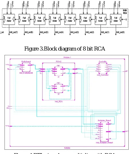
Figure 3.Block diagram of 8 bit RCA
Figure 4.RTL view-Array multiplier with RCA
III. ARRAYMULTIPLIERWITHDELETIONSCHEME
.Theproposed method involves deletion, which is done at the stage of partial product generation section. whenever a value of multiplier is ‘0’ ,the multiplier doesn’t added to the accumulator. Only bit level shifting was done at this stage. In other words the partial product bits are deleted when the mulplier bit is ‘0’. If the multiplier bit is ‘1’, then the multiplicand is added to the accumulator and finally the partial products is carried out by the carry propagation addder
A. Shift and add multiplier
[image:3.612.200.413.570.700.2]The general architecture of the shift and add multiplier for a 8-bit multiplication is shown in the figure below[6]. Depending on the value of multiplier LSB bit, a value of the multiplicand is added and accumulator. At each clock cycle the multiplier is shifted one bit to the left and its bit value is checked either it is ‘0’ or ‘1’. When the bit value of multiplier is ‘0’, the concerned partial product is not generated, only a bit level shift operation is performed in the accumulator register. If the bit value is ‘1’, then the multiplicand is added to the accumulator and one significant bit level is shifted to the left for receiving the next partial product. After all the multiplier bits have been tested, the partial product is added and the resultant product is stored in the accumulator. The accumulator is 2N (M+N) in size and initially the N, LSBs contains the Multiplier. The delay is N cycles maximum.
IV. ARRAYMULTIPLIERWITHCARRYSELECTADDER
[image:4.612.201.421.193.300.2]The project is about the implementation of array multiplier with deletion scheme and carry select adder for improving speed of operation of the multiplier. Array multiplier with deletion scheme offers significant improvement in area, delay & power. The combination of these two will got the preferred result. In the proposed method, the carry select adder circuit is employed instead of carry propagation adder circuit logic and thereby a set of adders could be replaced by one carry select adder. While implementing this proposed method experimentally, time of operation and area can saved.
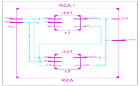
Figure 6.Block diagram of 8 bit RCA
A. Multiplier Using Carry Select Adder
Carry Select Adder (CSLA) is one of the fastest adders used in many data-processing processors to perform fast arithmetic functions[2][3]. From the structure of the CSLA, it is clear that there is scope for reducing the delay in the CSLA. The CLSA is used in many computational systems to alleviate the problem of carry propagation delay by independently generating multiple carries and then select a carry to generate the sum[7][8]. In this project carry select adder is used to reduce the delay and area. Figure shows the block diagram of the multiplier by using carry select adder. Here the main difference is the carry propagation adder is replaced by carry select adder. n x n bits multiplier computes the 2n bits output as a weighted sum of partial products. For the addition of partial products carry select adder is used it will reduce the time of operation.
Figure 7.Block diagram of the Array multiplier by using carry select adder
B. Block Details
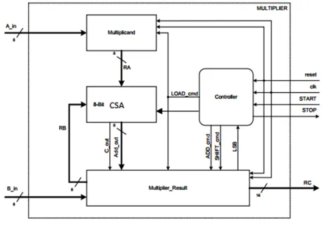
The design was implemented using a mixture of both structural design and RTL level design. In each case the choice of style is described. The block diagram showed in Figure details the breakdown of VHDL modules.
[image:4.612.190.420.464.624.2]shifting and counting operations
2) Multiplicand block design : The Multiplicand block is composed of 8 D Flip-Flop blocks, which store A byte for processing during the complete multiplication cycle. The register is loaded with the LOAD command signal from the Controller. 3) Multiplier/Result block design : The Multiplier/Result block stores the multiplier (.B. byte) as well as the accumulated
output of the adder. It allows the register to be logically shifted right and provides one of the adder’s inputs. The Multiplier/Result block consists of a 17-bit shift register and a multiplexer in order to provide this functionality.
4) Adder design : The adder design is the most influential part of the multiplier in terms of the area and speed achievable. This is due to the large iterations of additions performed in the multiplication cycle
5) Multiplier design : The complete multiplier is simply a top-level module which instantiates all the lower level functional modules described in the previous sections.
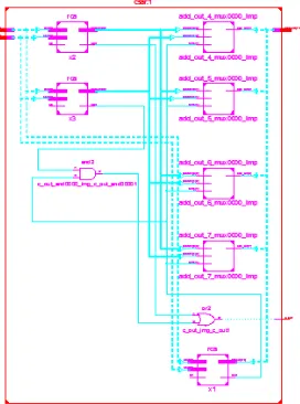
[image:5.612.260.396.326.509.2]6) Carry select adder : The concept of the carry-select adder is to compute alternative results in parallel and subsequently selecting the correct result with single or multiple stage hierarchical techniques. In order to enhance its speed performance, the carry-select adder increases its area requirements. In carry-select adders both sum and carry bits are calculated for the two alternatives: input carry “0” and “1” Once the carry-in is delivered, the correct computation is chosen(using a MUX) to produce the desired output. Therefore instead of waiting for the carry-in to calculate the sum, the sum is correctly output as soon as the carry-in gets there. The time taken to compute the sum is then avoided which results in a good improvement in speed.
[image:5.612.211.424.361.675.2]Figure 8.RTL View of Carry Select Adder
V. SOFTWAREUSED
The project is carried out in VHDL Language. And it was simulated in XILINX ISE 12.2 (Integrated Software Environment) design suit. Xilinx ISE is a software tool produced by Xilinx for synthesis and analysis of HDL designs, enabling the developer to synthesize ("compile") their designs, perform timing analysis, examine RTL diagrams, simulate a design's reaction to different stimuli, and configure the target device with the programmer.
VI. EXPERIMENTALRESULT
Table 1.Experimental Result
BIT LENGTH 8BIT DELAY (ns)
ARRAY MUL WITHOUT DELECTION SCHEME
220.5
ARRAY MUL USING CPA 184.3
ARRAY MUL USING CSLA
145.7
VII.CONCLUSION
advantage is delay increases slowly as the input bit increases. In this paper deletion is limited to partial product generation area so the result becomes absolutely free of error.
REFERENCES
[1] Srivastava, P.; Vishant, V.; Singh, R.K.; Nagaria, R.K., "Design and implementation of high performance array multipliers for digital circuits," Engineering and Systems (SCES), 2013 Students Conference on , vol., no., pp.1,5, 12-14 April 2013
[2] Basanth kumar mohanty and sujith kumar patel,”Area-Delay-Power Efficient Carry Select Adder” in IEEE Trans. On circuits and systems-II Express Briefs,Vol 61,No.6 June 2014.
[3] Low-Power and Area-Efficient Carry select Adder by B.Ram Kumar and Harish M Kittur in IEEE Transactions on Very Large scale Integration(VLSI) Systems, Volume 20 No.2, February 2012
[4] Gurumurthy, K.S.; Prahalad, M.S., "Fast and power efficient 16×16 Array of Array multiplier using Vedic Multiplication," Microsystems Packaging Assembly and Circuits Technology Conference (IMPACT), 2010 5th International , vol., no., pp.1,4, 20-22 Oct. 2010
[5] Ravi, N.; Subbaiah, Y.; Prasad, T.J.; Rao, T.S., "A novel low power, low area array multiplier design for DSP applications," Signal Processing, Communication, Computing and Networking Technologies (ICSCCN), 2011 International Conference on , vol., no., pp.254,257, 21-22 July 2011 [6] Sahoo, S.K.; Shekhar, C., "Delay optimized array multiplier for signal and image processing," Image Information Processing (ICIIP), 2011 International
Conference on , vol., no., pp.1,4, 3-5 Nov. 2011
[7] K.Swarnalatha, S.Mohan Das and P.Uday Kumar “An Efficient Carry Select Adder With Less Delay And Reduced Area Using Fpga Quartus Ii Verilog Design ” International Journal of Science, Engineering and Technology Research (IJSETR) Volume 2, Issue 8, August 2013