Technology (IJRASET)
The Modified SEPIC Converter with Extra Boost
Unit and Without Coupling Inductor for PV
Application
Akshay Kumar D1, Dr. R. V. Parimala2 1
PG student Department of Electrical and Electronics Engineering, BNMIT, Bengaluru, INDIA. 2
HOD, Department of Electrical and Electronics Engineering, BNMIT, Bengaluru, INDIA.
Abstract-In this paper, the modified SEPIC converter with extra boost circuit and without coupling inductor is proposed for PV application using perturb and observe mppt algorithm. The proposed DC-DC converter has only one MOSFET switch with minimum voltage stress and this reduces the complex circuit design. The proposed converter is connected in between PV panel and load to obtain high voltage without extreme duty ratio. In this paper input voltage of 40V is obtained from PV panel is fed to converter in order to obtained output voltage of 400V with switching frequency of 100kHz. Thecircuit operation and passive parameter design of this proposed converter are discussed in details.
Keywords-SEPIC, MPPT algorithm,PV panel.
I. INTRODUCTION
Today, Indian energy scenario is mainly focuses on harvesting and maximum usage of green energy resources such as fuel cell, wind energy and solar energy etc, due to depleting nature of conventional fuels and increasing energy demand of society. In order to meet demand the high voltage DC –DC converters must be incorporate between PV panels and grid. As PV panel have less output voltage of about 12 to 40 V, these must be boost to 440 V for grid applications. Therefore, DC-DC converter having high voltage output required to be placed between PV array and high voltage dc grid.Unfortunately, conventional high voltage converter are not available because of high duty ratio and complex circuit design .In order to have high voltage converters, following type of converter have been proposed by 1) addition of switching capacitors or switching inductors to conventional converters[1-2]; 2) series connection of outputs [3-4];3) combining output of several conventional converters[5];4) integrating coupled inductor and voltage-doubling circuit or switching inductor[6-11]; 5) interleaving technique[12-13].however ,all of these techniques have their own demerits. High setup gain, simple modified control structure, higher efficiency and minimum voltage stress are the features still needed.
In this paper, the modified SEPIC converter with extra boost unit circuit and without inductor coupled is proposed forPV application using Perturbs and observe MPPT algorithm.It produces higher voltage ratio, reduced voltage stress of switch and continuous operation of input current.
II. PV CELL MODELING AND MPPT ALGORITHM
A. PV CELL MODELLING
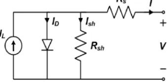
The circuit configuration of PV cell is shown in fig.1.In this circuit Rs is series resistance of PN junction cell and Rsh is shunt
resistance which is inversely in relation with leakage current to the ground. ID and Ish are diode current and shunt leakage current,
[image:2.612.220.389.618.701.2]where output current I is obtained by applying KCL.
Technology (IJRASET)
= −( + ) (1)
Above equation is simplified by taking + = Io and hence equation becomes
IL= − (2)
Photon current is generated on absorption of solar radiation; hence photocurrent is directly proportional to variation of solar irradiance and temperature, is given by.
= ( + ∆ ) (3)
Where Iscr is short circuit current at normal conditions (250C and 1000w/m2), ki is short circuit current temperature coefficient. G is
solar irradiance in W/m2 and Gr is nominal irradiance in normal conditions (250C and 1000w/m2).ΔT is difference ofoperating
temperature and nominal operating temperature (T – Tref).Reverse saturation current is given by.
= ∗ ∗ ∆ (4)
Where Irs is reverse saturation current for nominal temperature and irradiance and Ego is band gap energy of semiconductor material, current I is given by
= − (exp ( )-1) – (5)
B. Perturb and observe algorithm
This method is widely used, the operating output voltage is sampled and then it changes the operating output voltage in the required direction and samples the dP/dV. If is positive, then it increases the output voltage towards the MPP till is negative. This
iteration is continues till the algorithm reaches the final MPP.This is not applicable when then solar irradiation various continuously. The voltage never reaches the required value, but perturbs in between the maximum power point (MPP).
III. OPEATION OF PROPOSED CONVERTER
The proposed converter circuit configuration is shown below in Fig.2,It is obtained from a conventional SEPIC converter ,where capacitance C1, inductance L1,diodes D1 and D2 ,forms an extra boost unit circuit, while capacitance C3, and diode D3 are forms an
clamping circuit for MOSFET switch S .For the study of proposed converter ,let the following assumptions are made :1) converter is operated in steady state mode.2) all components are ideal;3) C2 andC3 are equal, Cout is more in order to make constant output voltage.
Fig.2.Single switch proposed converter.
Mode I [t0-t1]: When t=t0, switch S is switch on. Diode D1isforward biased, while diodes D2, D3 and D4 are reverse biased. The circuit
configuration and direction of current in this mode is shown in Fig. 3.Intitialy assumed that all capacitors are fully charged, in this mode, the input voltage Vinenergizes the inductor L1 viaD1 and switch S. Then the inductor voltage VL1 across L1 isVin. The capacitor
Technology (IJRASET)
viaswitch S, and then the inductor voltage VL3across L3 (VC3-VC2). So, the inductor currents iL1, iL2 and iL3linearlyincrease. The
capacitor Cout gives stored energy to the load R, and makes the output voltage Voconstant. When t=t1, Switch s is turned off, Mode I
[image:4.612.208.391.116.219.2]completed.
Fig .3.Circuit configuration of mode I in CCM.
Mode II [t1-t2]: When t=t1, switch S is turned off. D1 is reverse biased, while D2, D3 and D4 are forward biased. The circuit
configuration and direction of current in this mode is shown in Fig.5. Capacitor C1 is charges by the input voltage Vinand inductor
L1 viaD2 and VL1 is (Vin-VC1). At the same time, Vin, L1 and L2charges C3viaD2, then VL2 is (VC1-VC3). Moreover, the stored energy
of Vin, L1, L2 and L3 supply to Coutand load R,and VL3 is equal to -VC2.So, the inductor currents iL1, iL2and iL3 decrease linearly.When
[image:4.612.219.390.309.390.2]t=t2, switch S is turned on and mode II is completed.
Fig .4.circuit configuration of mode IIin CCM.
From inductor voltage second balanced principle, we have
D Vin= (1-D) (VC1-VIn) (6)
DVC1= (1-D) (VC3-VC2) (7)
D (VC3-VC2) = (1-D) VC2 (8)
Assuming capacitor voltage is constant during steady state operation from Equation (6), (7), (8), capacitor voltages are,
Vin= (1-D)VC1 (9)
VC1= (1-D)VC3 (10)
VC2=DVC3 (11)
During stage II
VO=VC2+VC3 (12)
Voltage gain in CCM mode is expressed by
= = ( )
( ) (13)
IV. PASSIVE PARAMETER DESIGN
A. Inductor design
From fig.3.inductor L1 current ripple in CCM is expressed by
∆ = (14)
=
∆ =∆% (15)
Technology (IJRASET)
=
∆ =∆% (16)
L3=
( )
∆ =∆% (17)
Fig.5.Theoretical wave form of CCM mode.
From Fig.4, the below current relationships are obtained, for mode I
iC3=-iL2 (18)
iC2=-iC3=iL3 (19)
From mode II
iC1=iL1-iL2 (20)
iC2=-iC3=iL3-Io (21)
Fromcapacitor ampere second balance principle, we have
IL2 = (1-D) IL3 (22)
IL3 = (1-D) IO (23)
If the power output Po, converter and resistive load R are known, as
IL1=Iin= (24)
IO= (25)
B. Capacitor design
Since capacitor C2 current is equal to that of C3 during mode I, the voltage potential of C2 or C3 is expressed by
∆ = (26)
∆V = (27)
Then
C2 = C3=∆ % (28)
Where, ∆V% = capacitor voltage ripple acceptance, in addition, the capacitorC1 and Coutare large in order to keep the constant output
voltage.
Technology (IJRASET)
From Fig.3 and Fig.4,VDS of the switch S in mode II is VC3, the diode voltage of D1 is VL2 in mode II or VC3 - VC1, that diode voltage
on D2 equals to VL2 or VC1 in mode I, diode voltage of D3 isVC3, and diode voltageD4 equals to the difference between Vo and VC2.
Then we have
VDS=VC3 =( ) = (29)
VD1 =VC3-VC1=( ) = (30)
VD2 = VL2 =VC1 = =
( )
( ) (31)
VD3 = VC3 = (32)
VD4 = Vo- VC2 = (33)
Since current via switch S in mode I is the summation of inductor currents iL1, iL2 and iL3, then peakcurrent in the switch will be
ISMAX =
∆%
( + + ) (34)
Both diode currentsiD1 and iD2 are part of inductor currentiL1, and then the peak diode currents of iD1 and iD2 will be
ID1MAX = ID2MAX =
∆%
(35)
It is known that iD3 = iL2 + iC2 = iL3 + iC3,iC2 = iC3in mode II,then peak current of diodeiD3 is
ID3MAX =
∆%
( + ) (36)
Finally, the current via D4 is output current Io
V. RESULTS AND DISCUSSION
In order to analyised the theoretical analysis, the operation of proposed Converter is simulated using MATLAB simulink and shown below Fig.6 and component design values are listed in table 1
Fig.6.MATLAB/simulink model for proposed converter.
The simulation waveforms of inductor currents IL1,IL2 and IL3, wave form of switching pulse generation and voltage across switch S
Technology (IJRASET)
Fig.7.Inductor current waveforms.
Fig.8. pulse generation and voltage waveform of switch S.
Fig.9.Output voltage waveform.
VI. CONCLUTION
In this paper,the modified SEPIC converter with extra boost unit circuit and without coupling inductor is proposed. It produces high voltage output without coupling inductor.Moreover, there is one MOSFET switch and the peak voltages of semiconductor switch are less than the output voltage, this makes the power switch with lower rating and all these features made this proposed converter suitable for PV application.
REFERENCES
[1] Xiong, Song, Siew-Chong Tan, and Siu-Chung Wong. “Analysis and design of a high-voltage-gain hybrid switched-capacitor buck converter”, IEEE Trans on
Circuits and Systems I: Regular Papers, vol.59, no.5, pp.1132-1141, May 2012.
[2] Axelrod, Boris, Yefim Berkovich, and Adrian Ioinovici. “Switched capacitor/switched-inductor structures for getting transformer less hybrid DC–DC PWM
Technology (IJRASET)
[3] Park, Ki-Bum, Gun-Woo Moon, and Myung-Joong Youn. “Non isolated high step-up stacked converter based on boost-integrated isolated converter”, IEEE
Trans on Power Electronics, vol.26, no.2, pp.577-587, Feb 2012
[4] Lee, J-Y, and Hwang, S-N, “Non-isolated high-gain boost converter using voltage-stacking cell”, Electronics Letters, vol.44, no.10, pp.644-646, Oct 2008
[5] Morales-Saldana, J. A., et al. “Multi loop controller design for a quadratic boost converter”, IET Electric Power Applications, vol.1, no.3, pp.362-367, 2007
[6] Zhao, Yi, et al. “High step-up boost converter with coupled inductor and switched capacitor”, 5th IET International Conference on Power Electronics,
Machines and Drives (PEMD 2010), 2010
[7] Spiazzi, Giorgio, Paolo Mattavelli, and Alessandro Costabeber. “High step-up ratio, fly back converter with active clamp and voltage multiplier”, IEEE Trans
on Power Electronics, vol.26, no.11, pp.3205-3214, Nov 2011
[8] Chen, Shih-Ming, et al. “A cascaded high step-up dc–dc converter with single switch for micro source applications”, IEEE Trans on Power Electronics, vol.26,
no.4, pp.1146-1153, Apr 2011
[9] Lee, Yuang-Shung, et al. “Quadratic boost converter with switched capacitor and coupled inductor for PV system applications”, 2013 IEEE10th International
Conference on. Power Electronic and Drive Systems (PEDS), 2013
[10] Hsieh, Yi-Ping, et al. “Novel high step-up DC–DC converter with coupled-inductor and switched-capacitor techniques”, IEEE Trans on Industrial Electronics,
vol.59, no.2, pp. 998-1007, Feb 2012
[11] Yang, Lung-Sheng, et al. “Novel high step-up DC–DC converter with coupled-inductor and voltage-doubler circuits”, IEEE Trans on Industrial Electronics,
vol.58, no.9, pp.4196-4206, Sep 2011
[12] Li, Weichen, et al. “Interleaved high step-up ZVT converter with built-in transformer voltage doubler cell for distributed PV generation system”, IEEE Trans
on Power Electronics, vol.28, no.1, pp.300-313, Jan 2013
[13] Henn, Gustavo AL, et al. “Interleaved-boost converter with high voltage gain”, IEEE Trans on Power Electronics, vol.25, no.11, pp. 2753-2761,Nov 2010.
BIOGRAPHY
AKSHAY KUMAR D1 obtained B.E (E&E) degree from AIT, Chikkamagaluru, under VTU, Belagavi and now pursuing M.TECH (CAID) from BNMIT, Bengaluru, under VTU Belagavi and area of interest are power electronics ,power system and control theory.Email id:[email protected]