Technology (IJRASET)
A Comparative Study of Scanning Electron
Microscopy (SEM) of Multilayer ZNS and CDS
Thin Films
Jitendra Singh1, Kapil Sirohi2, Pushpendra Singh3, Vishal Kumar Sharma4
1
Dept.of Physics,K.G.K.College,Moradabad (U.P.)
Abstract: The first thin solid films were obtained by electrolysis in 1864, B White Bunsen and Grover obtained metallic film in the year 1852, by thermal evaporation on explosion of a current carrying metal wire. The usefulness of optical properties of metal films and scientific curiosity about the behavior of two dimensional solid have been responsible for the immense interest in the study of the science and technology of thin films.In this paper we shall study the SEM of multilayer Zns and CdS thin films. Key Words:- Scanning Electron Microscopy(SEM),Multilayer Zns and CdS thin films
I. INTRODUCTION
The sulphide semiconductors are one of the most extensively investigated semiconductor in thin film form and a large variety of deposition techniques have been utilized to obtain solar cells.
ZnS is the II–VI family semiconductor, has wide band gap (3.65 eV) at room temperature and large excitation binding energy 60 meV, ZnS is an attractive semiconductor material especially in electronic and optoelectronic application. The dielectric constant of ZnS (wurtzite structure) is 8.75 at lower frequencies and 3.8 at higher frequencies. The molecular mass is 81.389 and the melting temperature is 1450 K.
ZnS was used by Ernest Rutherford and others in the early years of nuclear physics as a scintillation detector, because it emits light on excitation by x-rays or electron beam, making it useful for x-ray screens and cathode ray tubes.It also exhibits phosphorescence due to impurities on illumination with blue or ultraviolet light.
Zinc sulfide, with addition of few ppm of suitable activator, is used as phosphor in many applications, from cathode ray tubes through x-ray screens to glow in the dark products.When silver is used as activator, the resulting color is bright blue, with maximum at 450 nm. Manganese yields an orange-red color at around 590 nm. Copper provides long glow time and the familiar glow-in-the-dark greenish color. Copper doped zinc sulfide (ZnS+Cu) is also used in electroluminescent panels .
Zinc sulfide is also used as an infrared optical material, transmitting from visible wavelengths to over 12 micrometres. It can be used planar as an optical window or shaped into a lens. It is made as microcrystalline sheets by the synthesis from H2S gas and zinc vapor
and sold as FLIR (Forward Looking IR) grade ZnS in a pale milky yellow visibly opaque form.This material when hot isostatically pressed (HIPed) can be converted to a water-clear form known as Cleartran (trademark). Early commercial forms were marketed as Irtran-2 but this designation is now obsolete.
The Cadmium sulphide films grown by vacuum evaporation technique has been used as gas sensors for detection of oxygen and with a direct band gap it serve as a window material for heterojunction solar cells.
Sharma, R.P. et al, showed that CdS /polyaniline composite thin films can form tunable band gap heterostructure with vacuum evaporation CdS thin film on to glass substrate.
Jayachandran, M. et al, prepared Polyaniline layers onto porous structure by in-situ electrode position and showed photoluminescence at room temperature with a maximum current density 20 mA/Cm2, a possibility of polyaniline as ohmic contact. Schlamp, M.C. et al, demonstrated improved efficiency in LED's made with CdS and CdSe core / shell type nanocrystal incorporated in semiconducting polymers.
together with CdS.
II. SAMPLE PREPARATION OF ZNS AND CDS
Thin films of ZnS have been prepared by vacuum deposition technique. For sample preparation Zinc Sulphide powder of 99.99%. purity was evaporated at about 115°C from a deep narrow mouthed molybdenum boat. Deposition was made on to highly cleaned glass substrate held at 200°C in a vacuum of 10-5 torr. The substrate was cleaned in aquaregia washed in distilled water and isopropyl alcohol (IPA). We have used glass substrate for the preparation of Zinc Sulphide.
Thin films of CdS have been prepared by vacuum deposition technique. For sample preparation Cadmium Sulphide powder of 99.99%. purity was evaporated at about 115°C from a deep narrow mouthed molybdenum boat. Deposition was made on to highly cleaned glass substrate held at 200°C in a vacuum of 10-5 torr. The substrate was cleaned in aquaregia washed in distilled water and isopropyl alcohol (IPA). We have used glass substrate for the preparation of Cadmium Sulphide.
III. SAMPLE PREPARATION OF POLY ANILINE
Thin film of polyaniline have been prepared by vacuum evaporation technique, polyaniline is usually prepared by redox polymerization of aniline using ammonium perdisulphate, (NH4)2 S2O2 as on oxidant. Distilled aniline (0.02 M) is dissolved in 300
ml of pre-cooled HC1 (l.0M) solution, maintained at 0-50°C. A calculated amount of ammonium perdisulphate, (0.05M) dissolved in 200 ml of HCl (1M), pre-coated to 0-50° C, is added to the above solution. The dark green precipitate (ppt) resulting from this reaction is washed with HC1 (l.OM) uptil the green colour disappears. This ppt is further extracted with terta-hydofuran and NMP (N-Methyl Pyrolidinone) solution by soxhelf extraction and dried to yield the emeraldine salt. Emeraldine base can be obtained by heating the emeraldine salt with ammonia solution. Simultaneously, separate salt solution is prepared by dissolving the MX (M=Metal and X=Halide) in distilled water. The solution is then slowly added to the precooled polymer solution with constant stirring. The composite is then dried in an oven, at high temperature, to get the conducting polymer in the powder form. This powder is vacuum evaporated on to highly cleaned glass substrate as well as metallic substrate.
IV. SCANNING-ELECTRON MICROSCOPY (SEM)
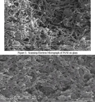
Scanning Electron Microscopy provides a direct structural evidence of the growth and perfection of the film. This is one of the most useful methods for the investigation of the surface topography, microstructural feature etc. It is based upon the fact that the electron are absorbed or diffracted at inhomogenities and thus reveals these inhomogenities as contrast effect. The secondary electrons are generated by the interaction of loosely bound electrons of the surface atoms. The emission of secondary electrons is sensitive to the incident beam direction and the topography of the surface layer. The contrast hence depends on the rate of secondary electron yields and the incident angle of primary beam to the surface being examined. The Scanning Electron micrographs obtained for Polyaniline on glass substrate and Polyaniline on ZnS thin film has been shown in fig.1 & 2, respectively. The results of the surface morphology are:
Polyaniline on ZnS shows a uniform morphology like pure Polyaniline film.
It shows some grain like structure due to the ZnS surface. The grains have become more regular and systematic for PANI on ZnS. The surface morphology of the samples has been investigated by scanning electron microscopy. To access the size and morphology the electron beam of 15 KV have been used the SEM image of CdS on glass substrate is shown in fig. (3). This indicate that the surface is smooth and grain boundaries are widens which are seen as thick black lines between the grains which are connecting together.
Technology (IJRASET)
[image:4.612.127.489.511.702.2]Figure 1: Scanning Electron Micrograph of PANI on glass
Fig.4. SEM image of Pani/CdS thin film on to glass substrate.
V. RESULTS AND DISCUSSIONS
The prepared films were subjected to scanning electron microscopy analysis to study surface morphology. The SEM studies of these thin films indicate a large increase in grain size up to 9
m, it is also observed that the substrate has a strong influence on thesurface morphology of the film. Pani on Zns shows a uniform morphology similar to pure polyaniline film. It shows some grain like structure due to the ZnS surface. The grains have become more regular and systematic for pani on ZnS. In case of CdS the surface is smooth and grain boundaries are widens which are seen as thick black lines between the grains which are connecting between while for pani/ CdS a large surface area and comparatively higher degree of crystalinity is observed.
REFERENCES
[1] R.P Sharma, M.S Raghuwanshi, and S.D Chavan Thin Films and Semiconductor laboratory research center. G.T Patil college Nandurbar [2] Jayachandram, M.; Paramasivam, M; Murali, K.R.; Trivedi, D.C.; Raghavan, M. Mater. Phys. Mech. 2001, 4, 143.
[3] Schlamp, M.C.; Xiaogang, P.; Alivisatos, A.P. J.Appl.Phys. 1997, 82, 5837. [4] Advincula, R.C et al. MRS Proceeding Fall 1997.
[5] N.F Foster etc. J.Appl. Phys.38, (197), 149.
[6] C. Hosokawa, H. Higashi and T. Kuaumoto, Appl. Phys; Lett. 62, 3238 (1993). [7] M. Berggren, G.Gustafgron, and T.Kusumto, Apll. Phys. Lett, 65, 1489 (1994). [8] P.E Burrrows amd S.R Forest, Appl. Phys. Lett 64, 2285 (1994).
[9] B.O Dabbousi, M.G Bawendi, O, Onitsuka, and MF Ritbbnr, Appl.Phys. Lett. 66, 1316 (1995).