2017 2nd International Conference on Communications, Information Management and Network Security (CIMNS 2017) ISBN: 978-1-60595-498-1
Design and Realization of FIR Digital Filter for
Optical IM/DD-OFDM System Using FPGA
Hao-ze LI, Hui-bin ZHANG, Jie ZHANG, Yong-li ZHAO,
Kai WANG and Yong SUN
State Key Laboratory of Information Photonics and Optical Communications, Beijing University of Posts and Telecommunications, China
Keywords: FIR Digital Filter, IM/DD, OFDM, FPGA.
Abstract. We present a finite impulse response (FIR) filter by using field programmable gate array (FPGA). It is designed in MATLAB, and we get filter coefficient from it. The implementation results showed decent performance in filtering.
Introduction
FIR digital filters are widely used due to their important role in various digital signal processing (DSP) applications. Digital filters modify signal characteristics in time domain, they are also used in many DSP systems to perform signal precondition, filtering, interpolation etc. [1]. Along with the advancement in orthogonal frequency division multiplexing (OFDM) technology, the DSP has become increasing popular over the years, the high-speed and high-flexibility realization of FIR filter with less power consumption has become much more demanding. For the last one decade, there has been a growing trend to implement DSP functions in FPGAs rather than application specific integrated circuits (ASIC) and DSP chips. FPGAs are preferred due to their high flexibility with the option to reconfigure, time-to-market, cost and performance [2].
For above reasons, several attempts have been made to realize reconfigurable architectures for FIR filters in FPGA platforms. However, those designs only focused on realization method and resource consumption [3], but didn’t consider the real-time communication systems which use FIR digital filter. In this paper, we’ll completely present a design and realization of FIR digital filter for intensity modulation/direct detection-OFDM (IM/DD-OFDM) system. This design adopts Xilinx zynq7020 FPGA to implement the system, including FIR digital filter. OFDM has been proposed for high-speed transmission over optical fiber due to the high utilization rate of frequency spectrum. In order to test performance of FIR filter, we also use optical fiber channel to transfer filtered OFDM symbols.
Filter Algorithm and Communication System Structure
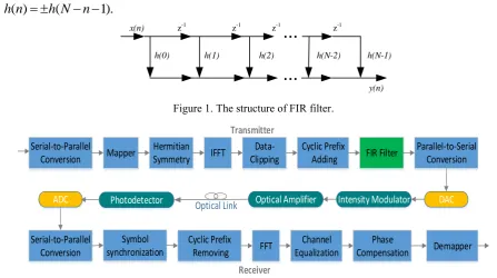
FIR digital filter is a key component in FPGA-based IM/DD-OFDM system, it can be realized conveniently in FPGAs because of its stability, linear phase and regular structure. FIR digital filter consist of finite sampling value, the output y(n) of an N-tap discrete-time FIR filter is represented as convolution form
1 0
( ) ( ) ( ) N ( ) ( ).
i
y n x n h n
h i x n i (1) where n represents the order of it, h(i) shows the fixed filter tap coefficients and x(n-i) is the input data which varies at every sampling instant. Furthermore, we can get its system function H(z) through z-transformation1 1
0
( ) N ( ) i [ (0) N (1) N ( 1)] N.
i
As can be known from Eq. 1 above, pole only exists in the origin point, so FIR filter has global stability. Besides, the filter has a linear phase, its impact sequence is real and satisfies odd symmetry or even symmetry, which can be expressed by Eq. 3.
( ) ( 1).
h n h N n (3) x(n) z-1 z-1 z-1 z-1
h(0) h(1) h(2) h(N-2) h(N-1)
y(n)
...
[image:2.595.69.517.124.374.2]...
Figure 1. The structure of FIR filter.
Serial-to-Parallel
Conversion Mapper
Parallel-to-Serial Conversion FIR Filter
Cyclic Prefix Adding Hermitian
Symmetry
Data-Clipping IFFT
DAC ADC Optical Amplifier Intensity Modulator
Serial-to-Parallel Conversion
Symbol synchronization
Phase Compensation Cyclic Prefix
Removing
Channel Equalization
FFT Demapper
Optical Link
Transmitter
Receiver Photodetector
Figure 2. The schematic diagram of optical IM/DD-OFDM system.
The regular structure of FIR filter is illustrated in Figure 1, this serial structure supports high speed operation and is easy to implement.
We use a schematic diagram to show transceiver structure of optical IM/DD-OFDM system, which is shown in Figure 2 In transmitter section, firstly, high-speed serial data stream transform into low-speed parallel bit stream through serial-to-parallel conversion, then map it with a certain modulation format. In order to perform intensity modulation after digital-to-analog converter (DAC) conveniently, we have to make sure that the output data of inverse fast Fourier transform (IFFT) is real, so it is necessary to process data with Hermitian symmetry module. To reduce peak to average power ratio (PAPR) of OFDM symbol we need data-clipping module. Adding cyclic prefix (CP) will improve ability to resist inter symbol interference (ISI) and inter carrier interference (ICI). The most important part of transmitter is FIR digital filter, since the DAC chip has zero-order hold characteristics and the output of the analog signal will remain a certain power of the mirror frequency, FIR filter can pre-filters the OFDM symbol to offset it. The performance of demodulation is very closely related to the performance of FIR filter.
which means we only need to do N/2 times multiplication to realize filter function rather N times. This operation is able to save the consumption of hardware resources, but also improve the processing speed.
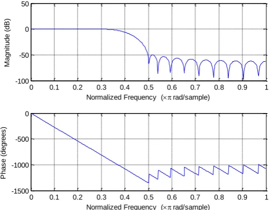
We choose Filter Design & Analysis Tool (FDATool) in signal process toolbox of MATLAB to make design of FIR filter. Filter’s essential parameter which can be obtained by analyzing the optical transmission system. The realization of it generally use window function method and equal corrugation approach. After comparison, Kaiser window function is more appropriate to our system. Passband boundary frequency p is 0.3, stopband boundary frequency s is 0.5, and stopband attenuation s is not less than 50dB. Obviously, is 0.2, the order approximation of the filter
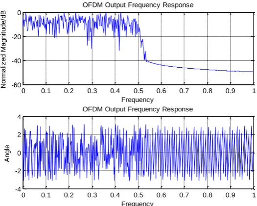
can be calculated with 30. So we can get suitable filter by using kaiserord function and fir1 function, then quantizing coefficients into canonic signed-digit, where nonzero elements are generally no more than two. Analyze compensation performance and modify parameters until we find the most appropriate coefficients for our system. After completion of design, we can analyze the performance of it by plot frequency response. The FIR’s magnitude, phase and normalized frequency relation chart is illustrated in Figure 3. As can be known from this figure, the characteristic of magnitude frequency response meets the requirement of optical IM/DD-OFDM system. Following the MATLAB simulation system model where can get OFDM output normalized magnitude frequency response and phase angle frequency response, which are shown in Figure 4. Where output normalized magnitude frequency response is consistent with the predicted result that output signal has already compensated the mirror frequency of DAC chip, and we can see from the figure that phase angle frequency response is homogeneous and steady. The final step in MATLAB is exporting coefficients as txt file. Then in order to import this file into FPGA we still need to change ‘txt’ filename suffix into ‘coe’.
0 0.1 0.2 0.3 0.4 0.5 0.6 0.7 0.8 0.9 1 -1500
-1000 -500 0
Normalized Frequency ( rad/sample)
P
h
a
s
e
(
d
e
g
re
e
s
)
0 0.1 0.2 0.3 0.4 0.5 0.6 0.7 0.8 0.9 1 -100
-50 0 50
Normalized Frequency ( rad/sample)
M
a
g
n
it
u
d
e
(
d
B
)
[image:3.595.155.424.404.613.2]
0 0.1 0.2 0.3 0.4 0.5 0.6 0.7 0.8 0.9 1 -60
-40 -20 0
OFDM Output Frequency Response
Frequency N o rm a liz e d M a g n it u d e /d B
0 0.1 0.2 0.3 0.4 0.5 0.6 0.7 0.8 0.9 1 -4
-2 0 2 4
OFDM Output Frequency Response
Frequency
A
n
g
le
Figure 4. OFDM output frequency response.
[image:4.595.164.427.77.287.2]d clk set q qf reset d clk set q qf reset d clk set q qf reset INV AND2 rsdff NOR2 rdy INV din(15:0) nd clk sclr rfd dout(37:0) chan_in(1,0) chan_out(1,0) rsdff rsdff FIR reader CS A2 A3 RD ai(37:0) b(15:0) VCC WR CS VCC VCC CLK RST ND w(15:0) RFD RDY A2 A3 CS RD R(15:0)
Figure 5. The realization of FIR filter in FPGA.
Table 1. FIR digital filter resource consumption.
Logic Utilization Used Available Number of Slice Registers 150 106400
Number of Slice LUTs 130 53200
Number of
LUT-FF pairs 62 218
[image:4.595.145.453.314.492.2]need to set input sampling frequency and clock frequency according to our OFDM system. The schematic diagram of implementation in FPGA is illustrated in Fig.5, where din represents input data and dout means output of FIR filter. ND signal is new data enable signal, input data will be sent into FIR calculation kernel when ND is high level. Obviously, CLK is the clock and RST is synchronous reset of this module. RST is active high and it can reset internal state machine of the filter but can’t empty the contents of the registers. RFD signal is filter work index signal, which means filter ignores any input signals when it is low level. RDY is output valid signal, bits width of output signal depends on taps, accuracy of filter and bits width of coefficient. Input data is controlled by ND signal, dout reads data in the meanwhile. Because input data bus is 16 bits, and output data is 38 bits, it is necessary for dout to read data repeatedly.
The proposed FIR digital filter has to be implemented on hardware at last. Programming file generation through Synthesize, Translate, Map, Place & Route processes in Xilinx ISE Design Suite, then it can be downloaded in target device. We can know about FIR digital filter resource consumption in Device Utilization Summary. The main logic utilization is shown in Table 1. That Number of Slice register, Slice LUTs, LUT-FF pairs and DSP48E1s are all sufficient for the filter. Comparing with other implementations, IP core use less hardware resource and has identical performance. We can also get filtered data from ChipScope Pro Analyzer through joint test action group (JTAG), the waveform we get is similar to Figure 4. Limitation of space prevents us from showing all the details of it.
Conclusions
In this paper, a FIR digital filter for optical IM/DD-OFDM system using FPGA is presented. The proposed design in MATLAB and implementation in FPGA is fully parameterizable, modular and scalable, so it is convenient to use IP core to complete our design. The implementation results of it showed decent performance in filtering and significant reduction in resource consumption.
References
[1] J. G. Proakis and D. G. Manolakis, Digital Signal Processing: Principles, Algorithms and Applications. Upper Saddle River, NJ: Prentice-Hall, (1996).
[2] G. R. Goslin, “A Guide to Using Field Programmable Gate Arrays (FPGAs) for Application-Specific Digital Signal Processing Performance”, XILINX, 1995.
[3] Patrick Longa and Ali Miri, “Area-Efficient FIR Filter Design on FPGAs using Distributed Arithmetic”, IEEE International Symposium on Signal Processing and Information Technology,