Flin-
HEWLETT
~~ PACKARD
HP 97060A Graphics Processor
Service Manual
Part No. 97060-90030
© Copyright 1984, Hewlett-Packard Company. All rights reserved.
This document contains proprietary information which is protected by copyright. All rights are reserved. No part of this document may be photocopied, reproduced or translated to another language without the prior written consent of Hewlett-Packard Company. The information contained in this document is subject to change without notice.
Restricted Rights Legend
Use, duplication, or disclosure by the Government is subject to restrictions as set forth in paragraph (b)(3)(8) of the Rights in Technical Data and Software clause in DAR 7-1 04.9(a).
ii
Printing History
New editions of this manual will incorporate all material updated since the previous edition. Update packages may be is'sued between editions and contain replacement and additional pages to be merged into the manual by the user. Each updated page will be indicated by a revision date at the bottom of the page. A vertical bar in the margin indicates the changes on each page. Note that pages which are rearranged due to changes on a previous page are not considered revised.
The manual printing date and part number indicate its current edition. The printing date changes when a new edition is printed. (Minor corrections and updates which are incorporated at reprint do not cause the date to change.) The manual part number changes when extensive technical changes are incorporated.
November 1983 ... First Edition
August 1984 ... First Edition with update
Warranty Statement
Hewlett-Packard products are warranted against defects in materials and workmanship. For Hewlett-Packard computer sys-tem products sold in the U.S.A. and Canada, this warranty applies for ninety (90) days from the date of shipment.* Hewlett-Packard will, at its option, repair or replace equipment which proves to be defective during the warranty period. This warranty includes labor, parts, and surface travel costs, if any. Equipment returned to Hewlett-Packard for repair must be shipped freight prepaid. Repairs necessitated by misuse of the equipment, or by hardware, software, or interfacing not provided by Hewlett-Packard are not covered by this warranty.
HP warrants that its software and firmware designated by HP for use with a CPU will execute its programming instructions when properly installed on that CPU. HP does not warrant that the operation of the CPU, software, or firmware will be uninter-rupted or error free.
NO OTHER WARRANTY IS EXPRESSED OR IMPLIED, INCLUDING BUT NOT LIMITED TO, THE IMPLIED WARRANTY OF MERCHANTABILITY AND FITNESS FOR A PARTICULAR PURPOSE. HEWLETT-PACKARD SHALL NOT BE LIABLE FOR CONSEQUENTIAL DAMAGES .
• For other countries, contact your local Sales and Support Office to determine warranty terms.
Table of Contents
Chapter 1. General Information
Introduction ... " 1-1 Description ... " 1-2 Environmental Specifications ... " 1-2 Electrical Characteristics ... " 1-3 Functional Specifications ... " 1-3 33/60 Hz Display Mode Selection ... " 1-4 Parallel Interface Pc Assembly Jumpers ... " 1-5 GPIO Interface Card Switch Settings ... " 1-6 Warnings, Cautions, and Notes ... " 1-6 Repair Philosophy ... " 1-6 Ac Components/Power Cord ... " 1-7 Voltage Options ... " 1-8 Grounding Requirements . . . .. 1-9 Safety ... 1-9
Chapter 2. Theory of Operation
Introduction ... " 2-1 System ... " 2-2 97060A Graphics Processor ... " 2-3 I/O ... 2-3 Processor . . . .. 2-3 Microcode PROM ... " 2-3 Processor Address Counters. . . .. 2-3 Screen Address Counters ... " 2-4 Pixel Memory. . . . .. 2-4 Pan/Zoom. . . .. 2-4 Color Map. . . . .. 2-4 Digital to Analog Converters ... " 2-4 Microcode Word Definition. . . . .. 2-5 Op Codes ... " 2-6
Chapter 3. Testing and Troubleshooting
Introduction ... " 3-1 Required Equipment ... " 3-1 Self Test ... " 3-1 Diagnostic LED Failure Indications ... " 3-2 Not Sequencing ... " 3-2 2901 Processor ... " 3-3 Data Bus ... " 3-3 Loop Counter ... " 3-3 I/O ... " 3-3 Scratch Pad ... " 3-3 Write/Read Back ... " 3-3 Signature ... " 3-3 RAM ... 3-4 Troubleshooting Hints ... " 3-5
iv
Chapter 4. Assembly Access
Introduction . . . 4-1 Electrostatic Discharge ... , , , , ... ' 4-2 Covers ... 4-4 Top Cover. . . . .. 4-5 Bottom Cover. . . . .. 4-6 Replaceable Assemblies ... 4-7 Parallel Interface Pc Assembly ... 4-8 GPIB Tablet Interface Pc Assembly. . . . .. 4-9 Controller Pc Assembly ... 4-10 Power Supply, - 5V, lOA ... 4-12 Power Supply,
+
5V, 20A ... 4-13 Fan ... 4-14Chapter 5. Replaceable Parts
Introduction . . . .. 5-1 Exchange Part. . . . .. 5-1 Non-Exchange Parts . . . .. 5-2 Figures 1-1 1-2 1-3 1-4 2-1 2-2 4-1 4-2 4-3 4-4 4-5 4-6 4-7 5-1 5-2 Tables 1-1 3-1 3-2 5-1 5-2
Controller Pc Assembly Jumpers ... 1-4 Parallel Interface Pc Asembly Jumpers. . . .. 1-5 Power Cords. . . . .. 1- 7 Power Supply Voltage Jumpers ... 1-8 System Block Diagram . . . .. 2-2 97060A Block Diagram ... 2-3 Top Cover . . . .. 4-5 Bottom Cover . . . .. 4-6 Parallel Interface Pc Assembly. . . . .. 4-8 GPIB Tablet Interface Pc Assembly ... 4-9 Controller Pc Assembly. . . . .. 4-11 - 5V, lOA Power Supply ... 4-12
+
5V, 20A Power Supply ... 4-13 Replaceable Parts, Top View. . . . .. 5-3 Replaceable Parts, Bottom View . . . .. 5-41-1
Chapter
1
General Information
Introduction
Note
Hewlett-Packard assumes no responsibility for customer repairs or modifications.
This manual contains servicing information for the Hewlett-Packard (HP) 97060A Graphics Proces-sor (hereinafter referred to as the 97060A). HP supports repairing the 97060A to the assembly level, that is, isolating the problem to the replaceable assembly. Then the defective assembly is exchanged for a new or rebuilt assembly.
This chapter contains general information about the 97060A and its servicing.
Additional information in this manual includes: • Theory of Operation
• Testing and Troubleshooting Procedures • Assembly Access Procedures
• Replaceable Parts
1-2 General Information
Description
The HP 97060A is a high-performance graphics processor. The 97060A has eight planes of 1024 X 1024 pixels.
Installation consists of unpacking, connecting power, connecting the RGB coax cables to the monitor, and connecting the interface cable to the GPIO card in the HP 9000 Series 500 computer.
The 97060A has refresh rate and voltage options which are preset at the factory. Refer to 33/60 Hz Display Mode Selection and Voltage Options which follow in this chapter for additional information.
Extensive self-test capability is built into the 97060A, and the READY light on the front panel gives a highly reliable indication that the self-tests have passed. Normally, the READY light turns on about 8 seconds after the ON light turns on at powerup. However, if a fault occurs, the READY
light does not turn on.
Environmental Specifications
Temperature: Humidity: Vibration: ( operating) Shock: (non-operating) Altitude: Drop Test:(non-operating, packaged)
EMI:
Safety:
- 40°C to + 75°C non-operating O°C to + 55°C operating
+ 40°C @ 95 % non-condensing operating Cycle range:
Amplitude (p-p): Sweeptime:
Dwell: Amplitude:
5-55-5 Hz 0.015 inch
1 minute per octave, 15 minutes total
10 minutes each resonance 0.125 inch @ 5-10 Hz 0.060 inch @ 10-25 Hz 0.015 inch @ 25-55 Hz
Magnitude: 30 G
Duration: 11 msec
No. of shocks: 18 (3 each on 6 surfaces)
Waveform: Half sine
Bench drop: 4-inch tilt
50,000 feet, 0-55°C, non-operating 15,000 feet, 0-55°C, operating
30 inches each face and corner
VDE Class A FCC Class A
UL 114 (Office Machines) UL478 (EDP)
CSA154 (EDP)
General Information 1-3
Electrical Characteristics
Rated Line Voltage:
Frequency Range:
Power Dissipated:
Supply Ratings:
Fuse:
Video:
Low Range: High Range:
47 to 66 Hz
90 to 132V ac 180 to 264V ac
<100W; 85W typical
+5V @ 20A
-5V @ 12A
4A Low Voltage Range, fast blow 6.3A High Voltage Range, fast blow
RS-343 compatible IV p-p with sync on Green. 0.7V video, 0.3V sync within 5%
Functional Specifications
Resolution:
Host Interface:
Tablet Interface:
Self Test:
Reset:
97060-90030, rev: 8/84
1024 X 768 @ 33 Hz interlaced 736 X 552 @ 60 Hz non-interlaced
Other options are soft programmable, such as 640 X 480,30 Hz, RS-170
Compatible with HP 27112A General Purpose 110 (GPIO) Interface Card with Option 001 interface cable
Compatible with HP 9111A Data Tablet
>90% of IC failures detected Data bus counter check
Bit slice register increment check Loop counter check
110 loop back check
Scratch pad RAM check, load with address Memory test: write allIs, Os, Is, Os; read back Write Mask, Write Data, check with read back Vector drawing test followed by signature read
1-4 General Information
33/60 Hz
Display Mode Selection
The 97060A may be set for either 33 or 60 Hz frame refresh rate (display mode), as follows:
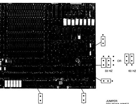
Access the controller pc assembly according to procedures in Chapter 4. Two jumpers near U291 on the controller pc assembly determine display mode selection. Ensure that both jumpers are in either the 33 Hz or the 60 Hz positions, depending on the monitor used. See Figure 1-1 for 33/60 Hz jumper positions. The other four jumpers are set at the factory and should not be changed. Ensure that they are in the positions shown in Figure 1-1.
•
[image:10.621.68.525.239.587.2]•
Figure 1-1. Controller Pc Assembly Jumpers
OR
•
I-ll-l.
~~.
• • •
60 HZ
JUMPER
General Information 1-5
Parallel Interface Pc Assembly Jumpers
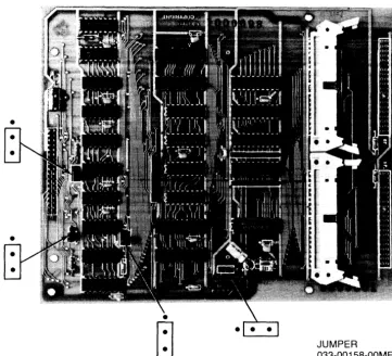
Four jumpers are contained on the parallel interface pc assembly (Figure 1-2). Three concern handshaking, the fourth concerns the INIT signal. The jumpers are set at the factory and should not be changed. Ensure that they are in the positions shown in Figure 1-2 .
•
•
~
JUMPER033-00158-00MET
[image:11.620.143.505.196.524.2]1-6 General Information
GPIO Interface Card Switch Settings
The HP 27112A General Purpose I/O (GPIO) Interface Card interfaces the HP 9000 Series 500 computer to the 97060A. The GPIO card switches should be set as follows. Note that a switch that is up is in the open position and represents a logic one; a switch that is down is in the closed position and represents a logic zero.
SWl: Sl through S8 - Down SW2: Sl, S2, and S5 - Up
S3 and S4 - Down
Warnings, Cautions, and Notes
Warnings, cautions, and notes are used in this manual. Warnings call attention to potential hazards for personnel. Cautions call attention to potential hazards for equipment. Notes emphasize impor-tant information or instructions.
Repair Philosophy
The 97060A is repaired at an assembly replacement level. Parts that are most commonly replaced are exchange parts and are on the Computer Support Division (CSD) exchange program. When an exchange part fails, it should be returned to CSD for repair, and a rebuilt part should be obtained. If
General Information 1-7
Ac Components/Power Cord
A detachable ac power cord plugs into an ac outlet to provide primary power to the 97060A. Other ac components are an on/off POWER switch, line fuse, line filter, fan, and wiring.
WARNING
IF IT IS NECESSARY TO REPLACE THE POWER CORD, THE RE-PLACEMENT CORD MUST HAVE THE SAME POLARITY AS THE ORIGINAL CORD. OTHERWISE, A SHOCK HAZARD MIGHT EXIST WHICH COULD RESULT IN INJURY OR DEATH. ALSO, THE EQUIPMENT COULD BE SEVERELY DAMAGED IF EVEN A RE-LATIVELY MINOR INTERNAL FAILURE OCCURRED.
[image:13.615.103.533.353.503.2]Power cords with different plugs are available for the 97060A; plug configurations are shown in Figure 1-3. Each plug has a ground connector. The cord packaged with the 97060A depends upon where the equipment is to be delivered. If your equipment has the wrong power cord for your area, please contact your local HP Sales and Support Office.
@
Australia
0
•
L•
NSouth Africa
&§j
0
•
•
€}
I
D
I
Country Part NumberE N L
• •
Australia 8120-1369•
L NDenmark 8120-2956 Denmark Europe Great Britain Europe 8120-1689 Great Britain 8120-1351 South Africa 8120-4211 Switzerland 8120-2104
<U>
QJ Q
United States 8120-1378L N United States 8120-0698
E
N L
•
Switzerland United States United States
120V 240V
NOTE: Plugs are viewed from connector end. Shape of molded plug may vary within country. Power cords supplied by HP have polarities matched to the power-input socket on the computer:
• L = Line or Active Conductor (also called "live" or "hot") • N = Neutral or Identified Conductor
• E = Earth or Safety Ground
Figure 1-3. Power Cords
1-8 General Information
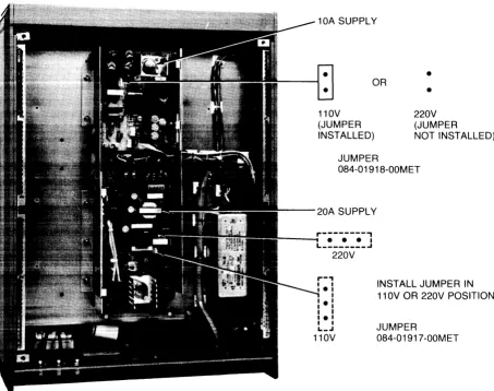
Voltage Options
The 97060A is configured at the factory for either 110V or 220V input line voltage. Table 1-1 lists the parts which are unique to the 110V and 220V options. Figure 1-4 shows power supply jumper configurations for the voltage options.
Table 1-1. Voltage Configuration Part Numbers
Description 110V
Power cord 8120-1378
Fan 050-00342-00MET
Line fuse 2110-0055
220V
Country dependent 050-00694-00MET 2110-0715
10A SUPPLY
•
OR
nov
(JUMPER INSTALLED)
•
220V (JUMPER
NOT INSTALLED)
JUMPER
084-01918-00MET
- - - 2 0 A SUPPLY
,.---,
- - -L ________ • • • I ..I
220V
INSTALL JUMPER IN 110V OR 220V POSITION
JUMPER
[image:14.613.70.523.293.651.2]084-01917-00MET
Figure 1-4. Power Supply Voltage Jumpers
General Information 1-9
Grounding Requirements
To protect operating personnel, the National Electrical Manufacturers' Association (NEMA) recom-mends that the 97060A chassis be grounded. The 97060A is equipped with a three-conductor power cable which, when connected to an appropriate power receptacle, grounds the computer chassis.
Safety
WARNING
LETHAL VOLTAGES ARE PRESENT INSIDE THE 97060A. OBSERVE ALL \VARNINGS IN THIS MANUAL, AND OBSERVE THE FOLLOWING SAFETY PROCEDURES.
• Do all possible operations with the 97060A unplugged from the power source.
• If installation, maintenance, or repair must be done with the 97060A energized, take the following precautions:
a. Never work alone in high-voltage areas. In case of accidental shock, a life may depend on rapid removal from the energized source and appropriate first -aid action.
b. Personnel working in high-voltage areas should know where to obtain respiratory resus-citation and/or cardiopulmonary resusresus-citation (CPR), in case a fellow worker needs assistance.
c. In case of burns, treat only after the person is breathing and has a normal heartbeat.
2-1
Chapter
2
Theory of Operation
Introduction
The HP 97060A is a high-performance raster graphics processor constructed from a mixture of MaS and bipolar Eel technology. The architectural components include:
• Bit-slice processor with 64-bit microword
• Megabyte of dynamic RAM (DRAM), organized as eight megabit planes of 1024 X 1024 • Integrated signature analyzer
• Hardware pan and zoom
2-2 Theory of Operation
System
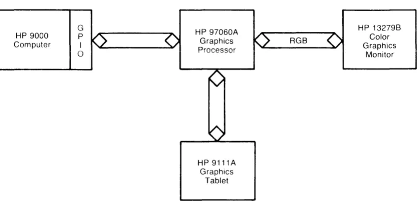
Communications with the HP 9000 computer is via the 16-bit parallel interface with the HP 27112A GPIO interface card and its Option 001 2.S-metre cable.
[image:18.613.78.489.233.436.2]An HPIB graphics tablet interface option is supported. allowing a local cursor to track the tablet stylus. The HP 9111A Data Tablet is the supported device.
Figure 2-1 shows a fully configured system.
HP 9000 Computer
G
P
I
o
HP 97060A Graphics Processor
HP 9111A Graphics
Tablet
RGB
Figure 2-1. System Block Diagram
HP 13279B Color Graphics
Monitor
The link between the computer and 97060A is bidirectional. The computer sends op codes and arguments in the 97060A syntax, and thus builds a picture in display memory. The computer may also read display memory or 97060A status.
The link to the graphics tablet is also bidirectional. although the tablet functions primarily as a sender. The tablet is software configurable and can be set under host control.
Theory of Operation 2-3
97060A Graphics Processor
Figure 2-2 is a block diagram of the 97060A hardware. Access to the dynamic RAM bit -map is shared by the processor and screen refresh circuitry.
To/From
GPIO I/O
Processor
I.l Code PROM
Internal 12-Bit Bus
Processor Address Counters
Other Circuitry
Screen Address Counters
1024 X 1024 X 8 Pixel Memory
Pan/Zoom Hardware
Color Map
Figure 2-2. 97060A Block Diagram
The functions of the 97060A blocks are as follows:
110
Digital to Analog Converters
Red Green Blue
This is the interface port to the HP 9000. The 97060A communicates with a "2-wire" handshake, PCTL and PFLG.
Processor
Composed of three 29018 bit slices, the 12-bit processor runs at a 220 ns cycle time.
Microcode PROM
[image:19.615.99.554.158.509.2]2-4 Theory of Operation
Processor Address Counters
These two 12-bit counters, one for X and one for Y, respond to the commands Load, Up/Down, and Count.
Screen Address Counters
These two counters, a 6-bit counter for X and a 10-bit counter for Y, only count up. However, they can be loaded with a start count other than zero to achieve the Pan function. They are automatically loaded on each vertical retrace. Counting can be prescaled by a modulo Zoom value.
Pixel Memory
Pixel memory consists of 128 DRAMs, 16 chips of 64K bits per plane. Memory is organized such that blocks of 16 adjacent pixels on a raster line are each contributed by a different DRAM output. Memory operates at a 220 ns write cycle and a 440 ns read cycle. The eight planes are indiVidually addressable through the Write Mask, Write Data, and Read Mask. These are each 8-bit registers with a flip-flop for each of the eight planes. Only when the Write Mask is set for a particular plane is its write enable line allowed to pulse. When written, the value of the particular Write Data flip-flop determines whether a 1 or a 0 is written. The Read Mask affects the planes read out and has no effect on data read by the processor.
In the following example, plane 0 is neither read nor written. Plane 1 is written with aI, and is viewed. Plane 2 is not written, but is viewed. Plane 3 is written with a 0, and viewed. Plane 4 is written with aI, and not viewed, and so forth.
Example:
Plane Write Mask Write Data Read Mask
0 0 1 0
1 1 1 1
2 0 1 1
3 1 0 1
4 1 1 0
5 0 0 1
6 1 0 1
7 1 1 0
Pan/Zoom
This circuitry contains modulo counters which essentially mirror the function of the screen address counters. Zoom is achieved by slowing down the entire pipeline from DRAM to the output digital-to-analog converters, causing pixel replication. Pan is achieved primarily by the screen address counters, but these only address 16 contiguous pixel blocks. To obtain a finer offset, a circular buffer is used as a programmable delay line.
Color Map
The 8-bit path through Pan/Zoom continues to the Color Map, a 256 X 24 RAM that allows the user to work with 256 colors Simultaneously from a palette of 16.7 million colors.
Digital to Analog Converters
Theory of Operation 2-5
Microcode Word Definition
The 64-bit microcode word resides in eight 16K PROMs, allowing 2048 steps of control memory. These PROMs are addressed by a 12-bit sequencer comprising two 2911As and a 2909A. The sequencer in turn is driven by microcode control bits and branching conditions from various sections of the hardware. The next section will explain these conditions in more detail.
The microcode word is subdivided into five major groups called fields:
• Control Field. These 13 bits of control lines regulate the processor address counters, the write enable generator for pixel memory, and other functions described below.
• Data Bus Source and Destination Control. Every instruction must specify a driver and a receiver for the internal data bus. This occurs even if no actual data transfer is required, in which case the destination is a dummy location. The sub-fields are:
Data Source Data Destination
3 bits 5 bits
• Conditional Branch Control. These 11 bits directly control the activity of the microcode se-quencer, which in turn selects the next microcode word decoded. There are three sub-fields:
Branch Type Condition Code
3 bits 8 bits
• Bit Slice ALU Controls. These 20 bits specify internal action of the three 2901B bit slice parts. There are five sub-fields:
External Carry/Borrow 3 bits ALU Destination 3 bits ALU Function 3 bits ALU Source 3 bits Register Address 8 bits
2-6 Theory of Operation
Op Codes
Unless othenvise specified, all writes to pixel memory observe the Write Data, Write Mask, and present Area Pattern. That is, a write in plane k occurs only if bit k of the Write Data Register and Write Mask Register are = 1 and the present Area Pattern function A(x,y) = 1.
Byte arguments are indicated by lower case, word arguments by upper case. Word arguments are read in the order: low byte, high byte.
The following are state variables:
PI (pointer 1) P2 (pointer 2)
WRITE DATA (also called "current color") WRITE MASK (determines planes written)
PATTERN REGISTER (including line and area patterns) READ MASK (planes viewed)
BLANK BLINK
CMAP (contents of 256 locations)
CONFIGURATION (33 Hz, 8 planes, tablet)
SETCORN, SETCSZ, FSIZE, CSPACE (character information) SZCUR (cursor size)
Mnemonic
AFILLI
AFILL2 <f>
ARC <I>
BLANK <b>
BLINK <b>
CHAR <cl,c2 ... cn>
CLEAR
CMAP <a,r,g,b>
COMPDR
CRTWR <r,d>
CSPACE <Ax,Ay>
CURS
DRAW
FFILL
FSIZE <Ax,Ay>
Theory of Operation 2-7
Hex Description
68 Read pixel at PI
69 62 4B 4D 6B 60 51 72 46 48 71 61 65 49
Do while neighbor color = PI pixel color Write neighbor with Write Data End
PI and P2 unmodified.
Read pixel at PI
Do until neighbor color = f Write neighbor with Write Data End
PI and P2 unmodified
Draw arc of length 1 using Write Data and center of curvature Pl. Begin at P2. P21eft at end of arc upon completion. 0<1<2047.
b is LSB of argument byte. If b = 1 then blank screen and give
proces-sor access. If b = 0 then return to screen-priority mode.
b is LSB of argument byte. If b = 1 then toggle plane 7 at 2 Hz, using Read Mask. If b = 0 then restore steady plane 7.
Draw text starting with PI pointing to the lower left corner of the 16 X 8 character cell. cl, c2, etc., are ASCII codes 0-127. cn is the ESC character (#27) and terminates text mode. See also SETCSZ, FSIZE, and CSPACE.
Control characters decoded:
CR Return to left margin
LF Move pointer down one line
BS Move pointer back one space ESC Exit text mode
Fill screen with Write Data.
Load color map location a with values r, g, and b.
Draw a vector between PI and P2 complementing present pixel values. Leave PI at P2. WRMASK and SETCOL not used.
Write the 6845-1 CRT Controller Register r with d.
Auto increment between successive characters. Apply increment Ax,Ay from lower left corner of cell, then apply transformation speci-fied by SETORN.
Draw cursor at Pl. Drawn in complement mode, with crosshair width and height as set by SZCUR. Automatically removed upon receipt of next op code. Write Mask and Area Pattern ignored.
Draw vector from PI to P2. Leave PI at P2.
Fill rectangle defined by diagonal Pl,P2. Approximately 16 times fast-er than RECT2; no pattfast-erns allowed.
2-8 Theory of Operation
Mnemonic
GRAFIN <f>
Hex Description
4A Set Graphic Input (from tablet). The argument (f), which is the GRA-FIN mode select byte, selects the current GRAGRA-FIN mode. It is one of the following:
o
Software INIT Mode. This mode resets all GRAFIN attributes to their default values and clears the coordinate queue. The offset and scale factors are also reset to their default values.The GPIB tablet interface pc assembly sends the following to the graphics tablet:
The DEVICE CLEAR signal.
The IN message--the Initialize (IN) messsage instructs the graphics tablet to run its self test and to return to the power-on condition.
The OF message - the Default (OF) message sets the graphics tablet to a predetermined power -on state.
Note
Refer to the Hewlett-Packard 9IIIA Graphics Tablet Us-er's Manual for information about messages sent to the graphics tablet.
I Local Cursor Control Mode. When in this mode, the tablet sends a continuous stream of x,y coordinates in the tablet's usual 8-bit, 6-byte format. The coordinates are buffered on the GPIB tablet interface pc assembly, and the stylus position is indicated by the cursor on the attached monitor. The cursor appears in the color complement of existing pixels.
A 5-byte message is sent to the host whenever the stylus on the tablet is depressed. The message format is shown in the following table. Bits I and 2 of byte I indicate the stylus position. When the stylus is depressed, the bits go high and the current stylus position is transmit-ted to the host.
Bit
Byte 7 6 5 4 3 2 1 0
I 0 I 0 0 0 sp sp 0
2 0 0 x5 x4 x3 x2 xl xO
3 0 0 0* 0* x9 x8 x7 x6
4 0 0 y5 y4 y3 y2 yl yO
5 0 0 0* 0* y9 y8 y7 y6
* Coordinates are those of the screen cursor, after applying offset and scaling. Transparent mode should be used if full tablet precision is required.
Theory of Operation 2-9
Mnemonic Hex Description
GRAFIN <f> 4A 2 Transparent Mode. Transparent mode allows the host to interact
( continued) directly with the graphics tablet, without converting the graphics tablet
data to the 97060A's 5-byte format. Full-duplex communications con-tinues until a delimiter (default: hex 80) is received to terminate Trans-parent mode. This mode is useful primarily in two cases:
Transparent mode may be used to run programs that were not specifi-cally written for use with the 97060A/9111A Graphics Tablet con-figuration. These programs may require graphics tablet data that has not been converted to the 97060A's 5-byte format.
Transparent mode may also be used to issue any of the commands described in the 9111A Graphics Tablet User's Manual, e.g., "RC;" or "RC" <LF>.
Note
When in Transparent mode, do not issue the Input Masks instruction using the Status Mask (S-mask) parameter. The S-mask parameter causes the graphics tablet to respond by activating SRQ (request service message) on the data line. The SRQ function on the data line is not supported on the GPIB tablet interface.
In Transparent mode, the graphics tablet sends one 6-byte message in response to each semicolon (;) it receives from the host.
In Transparent mode, all responses from the 9111A are padded to an even number of bytes. Responses that would normally have an odd byte count have a null character (OOH) appended to the end.
Commands sent to the tablet may be padded with as many ASCII space characters (20H) as desired. These are filtered from the charac-ter stream and not sent to the 9111A.
3 Set Offset and Scale Factors Mode. The device coordinates are subjected to an offset and scale operation in the 97060A for cursor position control. The next eight bytes specify the following in two's complement format:
1 - x offset low byte 2 - x offset high byte 3 - x multiplier fraction 4 - x multiplier integer 5 - y offset low byte 6 - y offset high byte 7 - y multiplier fraction 8 - y multiplier integer
2-10 Theory of Operation
Mnemonic Hex Description
GRAFIN <f> 4A 5 Sample Position - Screen Coordinates. This instruction causes the
(continued) full device status message to be sent to the host regardless of the
device's status message value. (No stylus switch closure is necessary.) See the preceding table under mode 1 for the full device status mes-sage format. The x,y values are returned in 97060A (5-byte) coordi-nates.
6 Sample Position - Tablet Coordinates. The full tablet coordinate mesage is relayed upon receipt of this command.
7 Set Mode Register. The mode register has the following bit defini-tions:
Bit IF = O(default) IF= 1
0 Wrap around Clip to screen Boundary
1 Level Buttons Edge Buttons
2 Button Xmit Button not Xmit
3 Report Button Depression No Output During
DUring GRAFIN 1 GRAFIN 1
These bits may be written as a group, by sending GRAFIN 7 followed by a byte with bits 0, 1, and 2 appropriately set and bit 7 = 1.
Alternately, one may set or clear an individual bit without modifying the others by setting bit 7 to a zero, bit 3 to zero or one (for clear or set, respectively) and bits 0, 1, and 2 to a pointer value (Le., 000 for bit 0, 001 for bit 1, and 010 for bit 2).
INIT 5E Soft Init. Receipt of this code causes the following:
Write Mask set to FF Write Data set to 0 Set solid pattern Set No Zoom and Pan
Turn on Read Mask for all planes Load Character Generator with ESC Clear line pattern counter
Clear Scratch pad RAM
Set default parameters in Scratchpad: Font Width = 8
Font Height = 16 Auto Increment Llx = 8 Auto Increment Lly = 0 Initialize tablet, delimiter, etc. Load Color Map with default values
The default Color Map values are most easily specified in terms of pixel value (address) for a given ratio of red, green, and blue:
pixel value =224*R +28*G +3*B where Rand G are chosen from the set (0,117,2/7, ... ,7/7) and B is chosen from (0,113,2/3,3/3)
MOVP1 52 Move PI from 10 x to hi x and from 10 y to hi y.
<lox,hix,loy,hiy>
MOVP2 53 Move P2 from 10 x to hi x and from 10 y to hi y.
Mnemonic
PATERN <p>
PIXBL T <Llx,Lly,d>
POLYC
Theory of Operation 2-11
Hex Description
50 Set pattern as specified in p. Area patterns remain in effect through all drawing operations except cursor and flash fill; in these instances drawing is in solid mode, i.e., line pattern O.
70
44
Bit
I
7I
6I
5I
4I
3I
2I
1I
a
I
\
.
I •• ' , ¥
.
mode invert line pattern
Bit 3 selects line pattern if a 1, area if a O. Bit 4 selects normal mode if 0, or swaps the foreground with background if = 1.
Mode: The pattern is considered a binary function of run length (line pattern) or x,y (area pattern). If the function = 1, then this is defined as Foreground (FG). Similarly, a value of
a
is defined as Background (BG). These definitions can be interchanged via bit 4 in the Pattern argument byte.Abbreviate the Write Data register byte as WD, and the Write Mask register byte as WM. Then the pattern mode options and mode bit values are:
Option Bit Value Meaning
FG~WD Bit 6=0 write all
FG~WD*WM Bit 6= 1 write selected
BG~BG*WM' Bit 7 = 1 zero selected
BG~ Bit 7 = 0; Bit 5 =
a
zero allBG~BG Bit 7=0; Bit 5= 1 no change
Copy a rectangle of pixels of width Llx and height Lly relative to PI to a rectangle of identical size relative to P2. The direction byte is used to prevent problems with overlapped regions; one must avoid writing a pixel before it is read.
Direction Bit
a
1 2 3 4IF=O IF= 1
normal swap x,y axes on destination
increment destination y decrement destination y increment destination x decrement destination x increment source y
increment source x
decrement source y decrement source x
Sub polygon delimiter command; used for concatenated polygons,
holes, etc. Inserted after POLYS, POLYV<XO,YO>,
POLYV<X1,Y1>, ... POLYV<Xk,Yk> to define a k + 1 vertex figure. The following POLYV<Xk+ 1,Yk+ 1>, POLYV<Xk+2,Yk+2>, ... POL YV<Xn,Yn>, POL YC will define another sub polygon of n-k vertices. This process may continue up to the stack limit (900 vertices).
2-12 Theory of Operation
Mnemonic
POLYF
POLYM <x,y>
POLYO
POLYS
POLYV <x,y>
PPAN
RDCONF
RDMASK <m>
RDR
RECTI
RECT2
RLFILL <~x>
RMOVPl <~x,~y>
RMOVP2 <ux.ily>
RPIXEL
SETCOL <c>
Hex Description
67 Polygon Fill. The current list of sub polygons in the stack will be scan converted and filled inclusive of edges. A parity fill occurs, meaning that only those regions are filled which are reached from the screen boundary via an odd number of edge crossings.
45 Polygon Move. The polygon edge from the previous point to x,y is flagged so as not to be drawn during POL YO. It is'in other respects treated as a normal polygon edge.
66 Polygon Outline. Outline the individual sub polygons, except where POL YM occurs.
56 Polygon Start. Clears polygon working area.
57 Polygon Vertex. Adds vertex X,y to the present sub polygon.
5B Set origin of display to PI. Confined to 16 pixel increments in X when no zoom. 5D 4C 6E 63 64 6A 54 55 6C 4E
Read Configuration. Upon receipt, the 97060A returns two bytes. The first is an 18 hex, signifying 33 Hz and Grafin installed. The second byte specifies the microcode release level as two hex numbers. For example, the byte 33 hex means version 3.3 microcode is installed.
Read Mask. The byte m specifies which planes are to be viewed, and has no effect on readback functions such as RDR, RPIXEL, AFlLL, COMPDR, or XDRAW. Overridden by blink function.
Read Rectangle. The 97060A returns a stream of pixel values from the rectangle defined by Pl,P2 beginning at the upper left corner and progressing left to right within top to bottom. Read is exclusive of right and bottom edges, so that the total number of pixels transferred is:
ABS(PIX - P2X)*ABS(PI Y - P2Y)
PI and P2 are not modified.
Outline the rectangle defined by Pl,P2 diagonal. PI and P2 are left unmodified.
Fill rectangle defined by P1,P2 diagonal, inclusive of edge. PI and P2 are left unmodified.
Run Length Fill. Write ilx successive pixels from PI, including PI, and leave PI one pixel past the sequence. O~~x~1023.
Relative move of Pl. Argument is 2s complement.
- 2048~~x,~y~2047.
Relative move of P2. Argument is 2s complement.
- 2048~~x,~y~2047.
Read pixel at Pl. A single byte is returned.
Theory of Operation 2-13
Mnemonic Hex Description
SETORN <d> 59 Set Character Orientation. The direction byte assigns meaning to the
lower three bits; these indicate character rotation and mirror inversion. Assume a relative 360-degree axis with ccw angle:
d Rotation Inversion
0 0 no
1 -90 yes
2 180 yes
3 -90 no
4 0 yes
5 90 no
6 180 no
7 90 yes
Transformations applied by CSPACE happen after this one.
SETCSZ <x,y> 58 Set Character Size. In text mode, characters are drawn within the constraints of FSIZE, CSPACE, SETORN, and this parameter. Its effect is to zoom characters via pixel replication, and the bytes x and y specify the replication number in the x and y directions prior to rota-tion. 0~x,y~255.
SIGRD 5C Read signature. A CRC polynomial is returned as two sorted bytes. In
non-interlace mode the two bytes are identical; in interlace mode they are odd and even field signatures.
SYNCH <f> 5F Wait until f fields have occurred before accepting further commands.
Useful for animation.
SZCUR <dx,dy> 47 Set Cursor Size. The cursor is displayed either in response to the CURS command, or during GRAFIN cursor tracking mode. It is a complementing crosshair with dimensions set by dx and dy of this command. The cursor dimensions will be twice these values. dx,dy~4095.
WPIXEL 60 Write pixel at PI using current color.
WRMASK <m> 4F Set Write Mask to byte value m; this determines the particular planes written for most drawing operations. It is ignored in cursor drawing and under certain pattern conditions.
WRR <bl,b2 ... bn> 6F Write Rectangle defined by PI and P2, beginning in the upper left and proceeding left to right within top to bottom. Fill is exclusive of the bottom and right edges, and the number of pixels expected is the same as for RDR. Pl,P2 unmodified.
XDRAW 73 Exclusive OR vector draw from PI to P2. The pixel written is the
EXOR of the previous value and the Write Data register. PI is left at P2 afterwards.
ZOOM <z> 5A Zoom screen via pixel replication by a count of z. The position of the
3-1
Chapter
3
Testing and Troubleshooting
Introduction
This chapter contains a list of the equipment required to test and troubleshoot the 97060A. It
describes the self test and all LED error indications.
Required Equipment
• Multimeter
• Monitor, color graphics, HP 13279B
Self Test
The built-in self test starts on powerup. Nine LEOs on the controller board indicate the results of self test. They are labeled 05 through 013. 012 indicates Hardware Clock (HWCLK) and 013,
Processor Clock (PROCCLK). If these LEOs are off, the clock circuit is faulty or -5 volts is not present. If the self test terminates without error, all nine LEOs are on and the READY LED on the front panel is lit.
3-2 Testing and Troubleshooting
Diagnostic LED Failure Indications
Table 3-1 defines the various failures indicated by the LEOs. A lit LED is indicated by an "X". Failures are more thoroughly described in text following the tables.
[image:32.615.97.472.205.577.2]LEOs 05 and 06 are not used to interpret an error. They are normally on but go off when an error occurs.
Table 3-1. Diagnostic LED Failure Indications
LEOs
05 06 07 08 09 010 011 012 013 Error
X X X Not Sequencing
X X X 2901 Processor
X X X X Data Bus
X X X Loop Counter
X X X X 110
X X X X Scratch Pad
X X X X X (Undefined)
X X X Write/Read Back
X X X X Signature
X X X RAM Row 0
X X X X RAM Row 1
X X X X RAM Row 2
X X X X X RAM Row 3
X X X X RAM Row 4
X X X X X RAM Row 5
X X X X X RAM Row 6
X X X X X X RAM Row 7
X X X X RAM Row 8
X X X X X RAM Row 9
X X X X X RAM Row A
X X X X X X RAM Row B
X X X X X RAM Row C
X X X X X X RAM Row D
X X X X X X RAM Row E
X X X X X X X RAM Row F
Not Sequencing
Testing and Troubleshooting 3-3
2901 Processor
The 2901 processor (U21, U22, U23) is faulty.
Data Bus
The self test counts up the data bus. This error is indicated if two data lines are shorted together or shorted to ground or
+
5 volts, or if two devices are driving the data bus at the same time.Loop Counter
The self test counts down the loop counter.
I/O
The microcode loops, sending Os and Is to the parallel interface pc assembly and reading them back.
Scratch Pad
Scratch pad test loops passing address to data and then writes. Then, address 1 contains data 1, address 2 contains data 2, etc. It then reads back. If an error occurs, the test stops. If there is no error, the data is complemented, written, and checked.
Write/Read Back
The test writes to memory and reads it back through the read back shift registers. If they don't match, an error is indicated. Possible causes of this error are outputs of two RAMs shorted together, RAS or CAS bad, or shift register bad.
Signature
This part of the self test displays the star pattern and checks it against the signature in PROM. If
3-4 Testing and Troubleshooting
RAM
If LEO 07 is lit, there is a RAM error. The combination of LEOs 08 through 011 indicate the row in which the error occurred. The address lines on a scratch pad RAM indicate which bank of RAMs is failing.
[image:34.615.76.496.265.508.2]Table 3-2 is a matrix which indicates the specific failing RAM. To find the failing RAM, determine the row according to LEOs 07 through 011 and determine the bank according to the high scratch pad address line as indicated by the U341 pins. For example, if LEOs 07, 09, and 011 are lit, and U341 pin 4 is high, U103 is the failing RAM. If more than one scratch pad address line is high, the problem is probably with the control lines, such as the address lines, write, enable, RAS, or CAS.
Table 3-2. Failed RAM Locater
LEOs
07 08 09 010 011 ROW
X 0
X X 1
X X 2
X X X 3
X X 4
X X X 5
X X X 6
X X X X 7
X X 8
X X X 9
X X X A
X X X X B
X X X C
X X X X 0
X X X X E
X X X X X F
* High scratch pad address line is determined as follows: AO - U341 pin S high
Al - U341 pin 6 high A2 - U341 pin 7 high A3 - U341 pin 4 high A4 - U341 pin 3 high AS - U341 pin 2 high A6 - U341 pin 1 high A7 - U341 pin 17 high
AO U18, U17, U16, U15, U14, U13, U12, U11, U10, U9, U8, U7, U6, US, U4, U3,
SCRATCH PAO AOORESS* Al A2 A3 A4 AS A6
49, 77 108 140 172 192 48, 76 107 139 171 191 47, 75 106 138 170 190 46, 74 105 137 169 189 45, 73 104 136 168 188 44, 72 103 135 167 187 43, 71 102 134 166 186 42, 70 101 133 165 185 41, 69 100 132 164 184 40, 68, 99 131 163 183 39, 67, 98 130 162 182 38, 66, 97 129 161 181 37, 65, 96 128 160 180 36, 64, 95 127 159 179 35, 63, 94 126 158 178 34, 62, 93 125 157 177
Testing and Troubleshooting 3-5
Troubleshooting Hints
The parallel interface pc assembly must be connected to the GPIO interconnect assembly for the 97060A to execute self test. If the GPIO host interface cables are not properly connected, the controller pc assembly hangs at an I/O error.
J3 is the 16-bit OMA into the 97060A, and J4 is the 16-bit OMA to the GPIO.
If LEOs 09 and 011 are on, indicating an I/O problem, and all others except clock LEOs 012 and 013 are off, check the following in the order indicated:
• Parallel interface pc assembly not plugged in • GPIO host interface cables not connected • Parallel interface pc assembly bad
• Controller pc assembly bad
During self test the 2901 processor writes a byte of Os and then a byte of Is to the parallel interface pc assembly, and then reads them back. If the handshake or data readback is bad, the 97060A hangs at I/O error.
4-1
Chapter
4
Assembly Access
Introduction
This chapter describes how to access all the replaceable 97060A assemblies. The table of contents of this manual lists the replaceable assemblies and the corresponding page numbers in this chapter where the access procedures are located. Read this introduction carefully before performing assem-blyaccess.
The procedures help you to disassemble the 97060A in order to access the assemblies. Reassembly procedures are the reverse of disassembly procedures. Special instructions required for reassembly are clearly noted.
This chapter is organized in several sections, as follows: • General Safety Procedure
• Electrostatic Discharge • Covers
• Replaceable Assemblies
The Covers subsection describes how to remove the top and bottom covers. The Replaceable Assemblies subsection describes how to access and replace assemblies.
The following tools are required to disassemble the 97060A:
• # 1 Pozidriv screwdriver • Flat -blade screwdriver • 1I4-inch nutdriver
• 3/8-inch nutdriver or wrench • 5/16-inch wrench
• Portable conductive antistatic kit, PN 9300-0933
CAUTION
4-2 Assembly Access
Electrostatic Discharge
Electrostatic discharge (ESO) causes failure in many PC assemblies, other assemblies, and compo-nents. Static electricity doesn't appear to be dangerous because much of the ESO that can cause component or assembly failure is too small to be felt. Humans can sense ESO of 3500-5000V. However, a discharge of 300V is enough to destroy some components.
Assemblies and equipment containing ESO-sensitive parts are often as sensitive as the most sensi-tive part they contain. Protecsensi-tive circuitry in these assemblies and equipment provides varying degrees of protection from ESO applied to their terminals. Such assemblies and equipment, how-ever, are still vulnerable to induced ESO caused by strong electrostatic fields or by contact of electrical connections or paths with a charged object.
Static damage is not always catastrophic. Sometimes a part slowly degrades, resulting in deteriorat-ing performance. For example, internal resistance changes cause speed or voltage changes. Results include intermittent or latch up problems (for example, a line printer prints bad data).
When disassembling the 97060A, a portable conductive field service antistatic kit should be used to eliminate ESO when handling or temporarily setting aside ESO-sensitive parts. The kit contains a wrist strap, antistatic mat, and ground cable.
Carefully observe the following procedures when disassembling the 97060A:
• Components, PC assemblies, and other assemblies and equipment should always be stored, transported, and shipped in antistatic or conductive containers.
• ESO-sensitive items must never be handled by ungrounded personnel, nor should they ever be stored on non conductive surfaces or near nonconductive materials.
• Field support should keep all replacement PC assemblies and components in antistatic or conductive bags. The failed board should be placed in a static-free bag for return to manufac-turing site.
• Removal of ESO-sensitive devices from an assembly must be done at a static-safe work station using all precautions. Suspect or rejected components, PC boards, and subassemblies are to be treated with the same care as good devices. Otherwise, further damage may result which prevents tracing the cause of the original failure.
Before removing devices from protective container:
a. Clear work area of static hazards such as plastic cups, bags, envelopes, and papers. b. Connect wrist strap.
c. Neutralize charges of ESO protective packaging containing an ESO-sensitive item and of tools by placing the packaged item on an ESO-grounded work bench surface to remove any charge prior to opening the packaging material. Alternately, charges can be re-moved by grounded personnel touching the package.
d. Ensure that the 97060A is properly grounded before inserting ESO-sensitive items. e. Remove ESO-sensitive item from ESO protective packaging using finger or metal
Assembly Access 4-3
• Place PC boards and components on table mat when not in static-shielding bags or other protective containers.
• Clothing must never contact ESD-sensitive parts. Wrist strap does not bleed off charges from clothing.
• Personnel handling ESD-sensitive items should avoid physical activities which are static pro-ducing in the vicinity of those items. Such activities include wiping feet and removing or putting on jackets or sweaters.
• Where ground straps cannot be used, personnel should ground themselves prior to removing ESD-sensitive items from their protective packaging.
• Tools and test equipment used in ESD-protective areas should be properly grounded; hand tools should not contain insulation on the handles or, if used, tools with insulated handles should be treated with a topical antistat.
• Ensure that all containers, tools, test equipment, and fixtures used in ESD-protective areas are grounded before and during use either directly or by contacting with a grounded surface. Grounding of electrical test equipment should be via a grounded plug, not through the con-ductive surface of the ESD-grounded work station.
• Do not assume that insulators are fully discharged when placed on a conductive work surface. Once the insulator is lifted off the surface, it retains its charge.
4-4 Assembly Access
Covers
WARNING
TURN POWER SWITCH OFF AND UNPLUG POWER CORD FROM AC OUTLET BEFORE REMOVING ANY ASSEMBLY.
The top and/or bottom covers must be removed to provide access to replacable assemblies. Follow the procedures and CAUTIONS carefully to avoid damaging covers.
CAUTION
Assembly Access 4-5
Top Cover
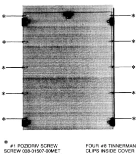
1. Turn off the POWER switch and unplug power cable from ac outlet.
2. Remove the 10 #1 Pozidriv screws and washers that attach top cover to chassis (Figure 4-1). 3. Lift cover slightly at the back and slowly pull cover away from the chassis, ensuring that the
RFI gasketing does not bind.
REASSEMBLY CAUTION
WHEN REPLACING TOP COVER, HOLD COVER AT A SLIGHT ANGLE AND INSERT COVER FLANGE INTO CHASSIS SLOT. THEN LOWER COVER INTO PLACE. THIS PREVENTS DAMAGE TO RFI GASKETING FROM SIDEWAYS MOTION OF COVER AND CHASSIS.
FROM OUTSIDE OF FRONT PANEL, VISUALLY CHECK RFI GASKETING FOR PROPER SEATING BEFORE TIGHTENING COV-ERSCREWS.
*--*---1
*---1
*---1
*--*
#1 POZIDRIV SCREW SCREW 038-01507-00MET WASHER 039-00367-00MET--*
--*
--*
--*
--*
[image:41.613.183.452.366.630.2]FOUR #8 TINNERMAN CLIPS INSIDE COVER
4-6 Assembly Access
Bottom Cover
1. Turn off the POWER switch and unplug power cable from ac outlet. Disconnect power cable and interface cables from 97060A.
2. Place 97060A on its top. Be careful to avoid damaging the top.
3. Remove the 10 # 1 Pozidriv screws and washers that attach bottom cover to chassis (Figure
4-2).
4. Lift cover slightly at the back and slowly pull cover away from the chassis, ensuring that the RFI gasketing does not bind.
REASSEMBLY CAUTION
WHEN REPLACING BOTTOM COVER, HOLD COVER AT A SLIGHT ANGLE AND INSERT COVER FLANGE INTO CHASSIS SLOT. THEN LOWER COVER INTO PLACE. THIS PREVENTS DAMAGE TO RFI GASKETING FROM SIDEWAYS MOTION OF COVER AND CHASSIS.
FROM OUTSIDE OF FRONT PANEL, VISUALLY CHECK RFI GASKETING FOR PROPER SEATING BEFORE TIGHTENING COV-ERSCREWS.
*--*----1
*---i
*--*
#1 POZIDRIV SCREW SCREW 038-01507-00MET WASHER 039-00367-00MET--*
--*
--*
--*
--*
[image:42.617.162.434.393.700.2]FOUR #8 TINNERMAN CLIPS INSIDE COVER
Assembly Access 4-7
Replaceable Assemblies
The following procedures describe the removal of replaceable assemblies. The reassembly proce-dures are the reverse of the removal proceproce-dures. If specific procedures are required for reassembly they are provided.
A list of the assemblies that have replacement procedures in this chapter follows: • Parallel Interface Pc Assembly
• GPIB Tablet Interface Pc Assembly • Controller Pc Assembly
• Power Supply, -5V, lOA • Power Supply, +5V, 20A • Fan
4-8 Assembly Access
Parallel Interface Pc Assembly
1. Prerequisite removal: • Top Cover
2. Disconnect both GPIO host interface cables from the parallel interface pc assembly (Figure
4-3).
3. Remove the four slotted screws and washers from the parallel interface pc assembly (Figure
4-3).
CAUTION
USE CARE WHEN REMOVING THE PARALLEL INTERFACE PC ASSEMBLY TO AVOID DAMAGING THE CONNECTORS WHICH INTERCONNECT IT WITH THE GPIB TABLET INTERFACE PC ASSEMBLY.
4. Lift the parallel interface pc assembly from the GPIB tablet interface pc assembly.
GPIO HOST INTERFACE CABLES 056-01119-00MET, 12-INCH 056-01120-00MET, 8.5-INCH
PARALLEL INTERFACE PC ASSEMBLY
080-00784-02M ET
SCREW
038-01473-00MET
WASHER
[image:44.615.130.488.351.707.2]039-00366-00M ET
Assembly Access 4-9
GPIB Tablet Interface Pc Assembly
1. Prerequisite removals: • Top Cover
• Parallel Interface Pc Assembly
2. Disconnect the GPIB cable from the GPIB tablet interface pc assembly (Figure 4-4).
[image:45.612.104.546.353.702.2]3. Remove the four slotted screws and washers from the GPIB tablet interface pc assembly (Figure 4-4).
CAUTION
USE CARE WHEN REMOVING THE GPIB TABLET INTERFACE PC ASSEMBLY TO AVOID DAMAGING THE CONNECTORS WHICH INTERCONNECT IT WITH THE CONTROLLER PC ASSEMBLY.
4. Lift the GPIB tablet interface pc assembly from the controller pc assembly.
GPIB TABLET INTERFACE PC ASSEMBLY 080-00841-05MET
STANDOFF 044-02040-00M ET SCREW
038-01473-00MET WASHER
039-00366-00M ET
Figure 4-4. GPIB Tablet Interface Pc Assembly
CREW
038-01473-00MET WASHER
039-00366-00MET
4-10 Assembly Access
Controller Pc Assembly
1. Prerequisite removals: • Top Cover
• Parallel Interface Pc Assembly • GPIB Tablet Interface Pc Assembly
CAUTION
RECORD ALL CABLE POSITIONS BEFORE DISCONNECTING CABLES FROM ASSEMBLY. NOTE ESPECIALLY THE R, G, AND B VIDEO CABLES AND THE POSITION OF THE LED CABLE CON-NECTOR.
2. Remove the power cable, LED cable, and the three video cables from the controller pc assembly (Figure 4-5).
3. Remove the four hex standoffs and washers from the controller pc assembly (Figure 4-5). 4. Remove the 12 slotted screws and washers from the controller pc assembly (Figure 4-5). 5. Bend cables out of the way and remove controller pc assembly from chassis.
REASSEMBLY CAUTION
*
POWER CABLE 056-01825-00MET
*
*
SCREW 038-01473-00MET WASHER039-00366-00M ET
Assembly Access 4-11
VIDEO CABLE 056-01806-00MET
CONTROLLER PC ASSEMBLY 080-01201-01 MET
STANDOFF 044-00056-00M ET WASHER
039-00367 -OOM ET
SLEEVE OVER STANDOFFS
UNDER CONTROLLER PC ASSEMBLY
[image:47.613.82.559.98.524.2]044-01745-00MET
4-12 Assembly Access
Power Supply, - 5V,
lOA
1. Prerequisite removal: • Bottom Cover
2. Disconnect connectors PI and P2 and ground wire from supply (Figure 4-6). 3. Remove the two slotted screws from the side bracket (Figure 4-6).
4. Loosen the two 5/I6-inch hex nuts opposite the removed screws to enable easy removal and replacement of the power supply (Figure 4-6).
5. Lift power supply by tabs and remove from chassis (Figure 4-6).
5/16"
HEX NUTS GROUND WIRE
P1
- 5V, 10A POWER SUPPLY
[image:48.615.77.536.265.671.2]048-01787-00MET SIDE BRACKET
Figure 4-6. - 5V, lOA Power Supply
SCREW
6-32 x 5/16" PAN HEAD, #1 POZIDRIV
TABS
SCREW
6-32 x 5/16" PAN HEAD #1 POZIDRIV
Power Supply,
+
5V, 20A
1. Prerequisite removal: • Bottom Cover
Assembly Access 4-13
CAUTION
TAG ALL WIRES AS YOU DISCONNECT THEM SO YOU CAN RECONNECT WIRES TO THE CORRECT TERMINALS.
2. Disconnect
+
OUT and -OUT wires and six wires from TB1 (Figure 4-7). [image:49.612.96.554.362.656.2]3. Remove the two slotted screws, washers, and 5/16-inch hex nuts from the side bracket (Figure 4-7).
4. Loosen the two 5/16-inch hex nuts opposite the removed screws to enable easy removal and replacement of the power supply (Figure 4-7).
5. Lift power supply by tabs and remove from chassis (Figure 4-7).
+OUT
SCREW
6-32 x 5/16" PAN HEAD #1 POZIDRIV
TAB
SIDE BRACKET
SCREW
6-32 x 5/16" PAN HEAD #1 POZIDRIV
TAB
Figure 4-7.
+
5V, 20A Power Supply-OUT
TBI
5/16" HEX NUTS (HIDDEN)
4-14 Assembly Access
Fan
1. Prerequisite removals: • Top Cover
• Bottom Cover
2. Disconnect the power cable from the fan.
5-1
Chapter
5
Replaceable Parts
Introduction
This chapter lists and locates all of the replaceable parts in the 97060A and provides information required to order replacement parts. All parts listed can be ordered from the Corporate Parts Centers except for the Controller Pc Assembly, an exchange assembly which is ordered from the Computer Support Division.
Figures 5-1 and 5-2 identify most replaceable parts.
Exchange Part
[image:51.618.175.474.485.529.2]The Controller Pc Assembly is the only part on the Computer Support Division (CSD) exchange program. When it fails, it should be returned to CSD for repair, and a rebuilt part should be obtained. Table 5-1 provides the part number.
Table 5-1. Exchange Part
Part Number Description
97060-69500 Controller Pc Assembly
5-2 Replaceable Parts
Non-Exchange Parts
[image:52.613.128.469.159.752.2]Table 5-2 lists the non-exchange parts.
Table 5-2. Non-Exchange Parts
Part Number Description
038-01507 -OOMET Screw, 6-32 X 3/4" flat head, #1 Pozidriv
039-00367 -OOMET Washer, #6 nylon, 0.03"
038-01473-00MET Screw, 6-32 X 5/16" pan head, slotted
039-00366-00MET Washer, #6 nylon, 0.06"
044-02040-00MET Standoff, 6-32 X 112", femalelfemale
044-00056-00MET Standoff, 6-32 X 112", malelfemale
044-01745-00MET Sleeve, standoff
033-00158-00MET Jumper, 2-pin
084-01918-00MET Jumper, lOA power supply configuration
084-01917-00MET Jumper, 20A power supply configuration
048-01787-00MET Power supply, - 5V, lOA
048-01788-00MET Power supply, + 5V, 20A
045-00347 -OOMET Switch, ac power, DPST, with cable
056-01825-00MET Power cable
056-01806-00MET Video cable, 26"
056-00512-00MET Coax cable
026-00417 -OOMET LED, red, ON
026-00418-00MET LED, green, READY
085-01189-00MET Front panel
085-01190-00MET Rear panel, 110V
085-01824-00MET Rear panel, 220V
080-00841-05MET GPIB tablet interface pc assembly
056-00673-02MET GPIB cable
080-00784-02MET Parallel interface pc assembly
056-01119-00MET GPIO host interface cable, 12-inch
056-01120-00MET GPIO host interface cable, 8.5-inch
080-01129-01MET GPIO interconnect assembly
042-01198-00MET Line filter
050-00342-00MET Fan, 110V
050-00694-00MET Fan, 220V
023-01387 -OOMET Area pattern PROM, U148
023-00916-01 MET Line pattern PROM, U149
023-00914-00MET Character set PROM, U150
078-01200-00MET Microcode kit PROM, U83-U90
0363-0170 RFI gasketing, strip fingers, 16 inches
2110-0715 Fuse, line, 6.3A, 220V
2110-0055 Fuse, line, 4A, 110V
2110-0003 Fuse, power supply, 3A
2110-0010 Fuse, power supply, 5A
8120-1351 Power cord, Great Britain
8120-1369 Power cord, Australia
8120-1689 Power cord, Europe
8120-1378 Power cord, U.S.A., 110V
8120-0698 Power cord, U.S.A., 220V
8120-2104 Power cord, Switzerland
8120-2956 Power cord, Denmark
8120-4211 Power cord, South Africa
VIDEO CABLE
LED CABLE
POWER CABLE -...i!!I.IPIi
Replaceable Parts 5-3
CONTROLLER PC ASSEMBLY
PARALLEL INTERFACE PC ASSEMBLY
...ofIM--GPIB TABLET
INTERFACE PC ASSEMBLY
GPIO HOST
INTERFACE CABLES
GPIB CABLE
GPIO
[image:53.613.139.569.148.522.2]INTERCONNECT ASSEMBLY
5-4 Replaceable Parts
- 5V, 10A POWER SUPPLY
3A FUSE
RFI
GASKETING
REAR PANEL
FRONT PANEL
[image:54.612.110.526.142.498.2]FAN
Figure 5-2. Replaceable Parts, Bottom View
POWER SWITCH
+ 5V, 20A POWER SUPPLY
5A FUSE
LINE FILTER
Part No. 97060-90030
E0884
Microfiche No. 97060-99030
Fli;-
HEWLETT
~~
PACKARD
Printed in U.S.A.