ANALOG-DIGITAL CONVERSION
1. Data Converter History
2. Fundamentals of Sampled Data Systems
3. Data Converter Architectures
4. Data Converter Process Technology
5. Testing Data Converters
6. Interfacing to Data Converters
6.1 Driving ADC Analog Inputs
6.2 ADC and DAC Digital Interfaces
6.3 Buffering DAC Analog Outputs
6.4 Driving ADC and DAC Reference Inputs
6.5 Sampling Clock Generation
7. Data Converter Support Circuits
8. Data Converter Applications
9. Hardware Design Techniques
I. Index
CHAPTER 6
INTERFACING TO DATA CONVERTERS
SECTION 6.1: DRIVING ADC ANALOG INPUTS
Walt Kester
Introduction
Before considering the detailed issues involved in driving ADCs, some general comments about trends in modern data converters are in order. Data converter performance is first and foremost, and maintaining that performance in a system application is extremely important. In low frequency measurement applications (10-Hz bandwidth signals or lower), Σ-∆ ADCs with resolutions up to 24 bits are now quite common. These
converters generally have automatic or factory calibration features to maintain required gain and offset accuracy. In higher frequency signal processing, ADCs must have wide dynamic range (low distortion and noise), high sampling frequencies, and generally excellent ac specifications.
In addition to sheer performance, other characteristics such as low power, single supply operation, low cost, and small surface mount packages also drive the data conversion market. These requirements result in a myriad of application problems because of reduced signal swings, increased sensitivity to noise, etc. As has been mentioned
previously in Chapter 3, the analog input to a CMOS ADC is usually connected directly to a switched-capacitor sample-and-hold (SHA), which generates transient currents that must be buffered from the signal source. This can present quite a challenge when selecting a drive amplifier. On the other hand, high performance data converters fabricated on BiCMOS or complementary bipolar processes are more likely to have internal buffering, but generally have higher cost and power consumption than their CMOS counterparts. The general trends in data converters are summarized in Figure 6.1.
Figure 6.1: Some General Trends in Data Converters
Higher sampling rates, higher resolution, excellent AC performance
Single supply operation (e.g., +5V, +3V, +2.5V, +1.8V) Lower power, shutdown or sleep modes
Smaller input/output signal swings Differential inputs/outputs
Maximize usage of low cost foundry CMOS processes Small surface mount packages
It should be clear by now that selecting an appropriate drive circuit for a data converter application is highly dependent on the particular converter under consideration.
Generalizations are difficult, but some meaningful guidelines can be followed. To begin with, one shouldn't necessarily assume that a driver amplifier is always required. Some converters have relatively benign inputs and are designed to interface directly to the signal source. In many applications, transformer drive may be preferable. Because there is practically no industry standardization regarding ADC input structures, each ADC must be carefully examined on its own merits before designing the input interface circuitry.
If an amplifier is required, a fundamental requirement is that it not degrade the dc or ac performance of the converter. One might assume that a careful reading of the op amp datasheets would assist in the selection process—simply lay the data converter and the op amp datasheets side by side, and compare each critical performance specification. It is true that this method will provide some degree of success; however in order to perform an accurate comparison, the op amp must be specified under the exact operating conditions required by the data converter application. Such factors as gain, gain setting resistor values, source impedance, output load, input and output signal amplitude, input and output common-mode (CM) level, power supply voltage, etc., all affect op amp performance to some degree.
It is highly unlikely that even a well written op amp datasheet will provide an exact match to the operating conditions required in the data converter application.
Extrapolation of specified performance to fit the exact operating conditions can give erroneous results. Also, the op amp may be subjected to transient currents from the data converter, and the corresponding effects on op amp performance are rarely found on datasheets.
Converter datasheets themselves can be a good source for recommended op amps and other application circuits. However, this information can become obsolete when newer op amps are introduced after the converter's initial release.
Analog Devices offers a parametric search engine which facilitates part selection (see http://www.analog.com). For instance, the first search might be for minimum power supply voltage, e.g., +3 V. The next search might be for bandwidth, and further searches on relevant specifications will narrow the selection of op amps even further. While not necessarily suitable for the final selection, this process can narrow the search to a manageable number of amplifiers whose individual datasheets can be retrieved, then reviewed in detail before final selection. Figure 6.2 summarizes the overall selection process.
Figure 6.2: ADC Driver (DAC Buffer) Selection Criteria
Amplifer DC and AC Performance Considerations
As discussed above, the amplifier (if required) should not degrade the performance specifications of the data converter. Today, ac specifications are generally paramount— especially with high-speed data converters. Chapter 2 of this book has discussed ADC and DAC specifications in detail, but it is useful to summarize the popular converter dynamic performance specifications in Figure 6.3.
Figure 6.3: Popular Converter Dynamic Performance Specifications
Signal-to-Noise-and-Distortion Ratio (SINAD, or S/N +D) Effective Number of Bits (ENOB)
Signal-to-Noise Ratio (SNR)
Analog Bandwidth (Full-Power, Small-Signal) Harmonic Distortion
Worst Harmonic
Total Harmonic Distortion (THD)
Total Harmonic Distortion Plus Noise (THD + N) Spurious Free Dynamic Range (SFDR)
Two-Tone Intermodulation Distortion Multi-tone Intermodulation Distortion
Some ADCs (DACs) do not require special input drivers (output buffers) The amplifier / transformer should not degrade the performance of the ADC (DAC)
AC specifications are usually the most important Noise
Bandwidth Distortion
Settling time from transient currents
Selection based on op amp data sheet specifications difficult due to varying conditions in actual application circuit with ADC (DAC):
Power supply voltages
Signal range (differential and common-mode) Loading (static and dynamic)
Gain and gain-setting resistor values Parametric search engines may be useful
ADC (DAC) data sheets often recommend op amps but may not include newly released products
For comparison, the fundamental op amp dc and ac specifications are summarized in Figure 6.4. Not all op amps will have these specifications, however they should certainly have most of them listed on the data sheet if the op amp is to be a serious contender for a high performance data converter application.
Figure 6.4: Key DC and AC Op Amp Specifications for ADC/DAC Applications Regardless of the importance of the ac specifications, the fundamental dc specifications must not be overlooked—especially in light of the implications of low voltage single-supply operation so popular today. The allowable input and output signal range becomes critically important in single supply applications as illustrated in the fundamental
application circuit shown in Figure 6.5.
Figure 6.5: Input/Output Signal Swing and Common-Mode Range is Critical in Single-Supply ADC Driver Applications
DC
Input/Output Signal Range Offset, offset drift
Input bias current Open loop gain Integral linearity
1/f noise (voltage and current) AC (Highly application dependent!)
Wideband noise (voltage and current) Small and Large Signal Bandwidth Harmonic Distortion
Total Harmonic Distortion (THD)
Total Harmonic Distortion + Noise (THD + N) Spurious Free Dynamic Range (SFDR) Third Order Intermodulation Distortion
+VS – + BIPOLAR INPUT R2 R1 ADC RT V1 VCM= V1 1 + R2R1 A1 A1 PROVIDES GAIN AND LEVEL SHIFTING INPUT CM RANGE
OUTPUT SWING
INPUT RANGE
The circuit of Figure 6.5 shows an op amp as a simple dc-coupled single-supply ADC driver which provides the proper gain and level shifting for the bipolar (ground-referenced) input signal such that it matches the input range of the ADC. Several
important points are illustrated in this popular circuit. The first consideration is the input range of the ADC, which in turn determines the output voltage swing requirement of the op amp. There are a number of single-supply CMOS ADCs with inputs that go from 0 V to the positive supply voltage. As will be illustrated shortly, even rail-to-rail output op amps cannot drive the signal completely to each rail. If, however, the ADC input range can be set so that the signal only goes to within a few hundred millivolts of each rail, then a single-supply "almost" rail-to-rail output op amp can often be used.
On the other hand, ADCs fabricated on BiCMOS or complementary bipolar processes typically have fixed input ranges that are usually at least several hundred millivolts from either rail, although many are not centered at the mid-supply voltage of VS/2.
Equally important is the input common-mode voltage of the op amp. In the circuit of Figure 6.5, the input common-mode voltage is set by V1, which level shifts the amplifier output to the correct value. Obviously, V1 must lie within the input common-mode voltage range of the op amp in order for the circuit to work properly.
These restrictions can become quite severe when operating the entire circuit on a single low-voltage supply, and therefore a brief discussion of rail-to-rail op amps follows in order to better understand how to properly select the drive amplifier. We will discuss the input and output stage considerations separately.
Rail-Rail Input Stages
Today, there is common demand for op amps with input common-mode voltage that includes both supply rails, i.e., rail-to-rail common-mode operation. While such a feature is undoubtedly useful in some applications, engineers should recognize that there are still relatively few applications where it is absolutely essential. These applications should be distinguished from the many more applications where a common-mode input range close
to the supplies, or one that includes one supply is necessary, but true input rail-to-rail operation is not.
In many single-supply applications, it is required that the input common-mode voltage range extend to one of the supply rails (usually ground). High-side or low-side current-sensing applications are typical examples of this. Many amplifiers can handle 0-V common-mode inputs, and they are easily designed using PNP differential pairs (or N-channel JFET pairs or PMOS pairs) as shown in Figure 6.6. The input common-mode range of such an op amp generally extends from about 200 mV below the negative rail (–VS, or ground), to within 1 V to 2 V of the positive rail (+VS).
Figure 6.6: PNP, PMOS, or N-Channel JFET Stages Allow Common-Mode Inputs to Include the Negative Rail
An input stage could also be designed with NPN transistors (or P-channel JFET pairs or NMOS pairs), in which case the input common-mode range would include the positive rail, and go to within about 1 V to 2 V of the negative rail. This requirement typically occurs in applications such as high-side current sensing.
A simplified diagram of what has become known as a true rail-to-rail input stage is shown in Figure 6.7. Note that this requires use of two long-tailed pairs, one of PNP bipolar transistors Q1-Q2, the other of NPN transistors Q3-Q4. Similar input stages can also be made with CMOS or JFET pairs.
Figure 6.7: A True Rail-to-Rail Input Stage
PNPs +VS N-CH JFETs +VS –VS –VS OR PMOS +VS Q1 Q2 Q3 Q4 –VS PNP OR PMOS PNP OR PMOS NPN OR NMOS
It should be noted that these two pairs will exhibit different offsets and bias currents, so when the applied common-mode voltage changes, the amplifier input offset voltage and input bias current does also. In fact, when both current sources remain active throughout most of the entire input common-mode range, amplifier input offset voltage is the
average offset voltage of the two pairs. In those designs where the current sources are
alternatively switched off at some point along the input common-mode voltage, amplifier input offset voltage is dominated by the PNP pair offset voltage for signals near the negative supply, and by the NPN pair offset voltage for signals near the positive supply. As noted, a true rail-to-rail input stage can also be constructed from CMOS transistors, for example as in the case of the CMOS AD8531/8532/8534 op amp family.
Amplifier input bias current, a function of transistor current gain, is also a function of the applied input common-mode voltage. The result is relatively poor common-mode
rejection (CMR), and a changing mode input impedance over the common-mode input voltage range, compared to familiar dual-supply devices. These specifications should be considered carefully when choosing a rail-to-rail input op amp, especially for a non-inverting configuration. Input offset voltage, input bias current, and even CMR may be quite good over part of the common-mode range, but much worse in the region where operation shifts between the NPN and PNP devices, and vice versa.
True rail-to-rail amplifier input stage designs must transition from one differential pair to the other differential pair, somewhere along the input common-mode voltage range. Some devices like the OP191/291/491 family and the OP279 have a common-mode crossover threshold at approximately 1 V below the positive supply (where signals do not often occur). The PNP differential input stage is active from about 200 mV below the negative supply to within about 1 V of the positive supply. Over this common-mode range, amplifier input offset voltage, input bias current, CMR, input noise voltage/current are primarily determined by the characteristics of the PNP differential pair. At the
crossover threshold, however, amplifier input offset voltage becomes the average offset voltage of the NPN/PNP pairs and can change rapidly.
Also, as noted previously, amplifier bias currents are dominated by the PNP differential pair over most of the input common-mode range, and change polarity and magnitude at the crossover threshold when the NPN differential pair becomes active.
Op amps like the OP184/284/484 family, utilize a rail-to-rail input stage design where both NPN and PNP transistor pairs are active throughout most of the entire input common-mode voltage range. With this approach to biasing, there is no common-mode crossover threshold. Amplifier input offset voltage is the average offset voltage of the NPN and the PNP stages, and offset voltage exhibits a smooth transition throughout the entire input common-mode range, due to careful laser trimming of input stage resistors. In the same manner, through careful input stage current balancing and input transistor design, the OP184 family input bias currents also exhibit a smooth transition throughout the entire common-mode input voltage range. The exception occurs at the very extremes of the input range, where amplifier offset voltages and bias currents increase sharply, due to the slight forward-biasing of parasitic p-n junctions. This occurs for input voltages within approximately 1 V of either supply rail.
When both differential pairs are active throughout most of the entire input common-mode range, amplifier transient response is faster through the middle of the common-mode range by as much as a factor of 2 for bipolar input stages and by a factor of √2 for JFET input stages. This is due to the higher transconductance of two operating input stages. The AD8027/8028 op amp family (Reference 1) has a pin-selectable crossover threshold which allows the user to choose the crossover point between the PNP/NPN input
differential pairs. Depending upon the state of the select pin, the threshold can be set for 1.2 V from the positive rail (select pin open) or 1.2 V from the negative rail (select pin connected to positive supply voltage).
Input stage gm determines the slew rate and the unity-gain crossover frequency of the
amplifier, hence response time degrades slightly at the extremes of the input common-mode range when either the PNP stage (signals approaching the positive supply rail) or the NPN stage (signals approaching the negative supply rail) are forced into cutoff. The thresholds at which the transconductance changes occur are approximately within 1 V of either supply rail, and the behavior is similar to that of the input bias currents.
In light of the many quirks of true rail-to-rail op amp input stages, applications which do require true rail-to-rail inputs should be carefully evaluated, and an amplifier chosen to ensure that its input offset voltage, input bias current, common-mode rejection, and noise (voltage and current) are suitable.
Output Stages
The earliest IC op amp output stages were NPN emitter followers with NPN current sources or resistive pull-downs, as shown in Figure 6.8A and B. Naturally, the slew rates were greater for positive-going than they were for negative-going signals.
While all modern op amps have push-pull output stages of some sort, many are still asymmetrical, and have a greater slew rate in one direction than the other. Asymmetry tends to introduce distortion on ac signals and generally results from the use of IC processes with faster NPN than PNP transistors. It may also result in an ability of the output to approach one supply more closely than the other in terms of saturation voltage. In many applications, the output is required to swing only to one rail, usually the negative rail (i.e., ground in single-supply systems). A pulldown resistor to the negative rail will allow the output to approach that rail (provided the load impedance is high enough, or is also grounded to that rail), but only slowly. Using an FET current source instead of a resistor can speed things up, but this adds complexity, as shown in Fig. 6.8B.
Figure 6.8: Some traditional Op Amp Output Stages
With modern complementary bipolar (CB) processes, well matched high speed PNP and NPN transistors are readily available. The complementary emitter follower output stage shown in Fig. 6.8C has many advantages, but the most outstanding one is the low output impedance. However, the output voltage of this stage can only swing within about one VBE drop of either rail. Therefore, a usable output voltage range of +1 V to +4 V is
typical of such a stage, when operated on a single +5-V supply.
The complementary common-emitter/common-source output stages shown in
Figure 6.9A and B allow the op amp output voltage to swing much closer to the rails, but these stages have much higher open-loop output impedance than do the emitter follower-based stages of Fig. 6.8C
In practice, however, the amplifier's high open-loop gain and the applied feedback can still produce an application with low output impedance (particularly at frequencies below 10 Hz). What should be carefully evaluated with this type of output stage is the loop gain within the application, with the load in place. Typically, the op amp will be specified for a minimum gain with a load resistance of 10 kΩ (or more). Care should be taken that the application loading doesn't drop lower than the rated load, or gain accuracy may be lost. It should also be noted these output stages can cause the op amp to be more sensitive to capacitive loading than the emitter-follower type. Again, this will be noted on the device data sheet, which will indicate a maximum of capacitive loading before overshoot or instability will be noted.
NPN NPN NPN PNP +VS +VS VOUT VOUT NMOS NMOS +VS VOUT (A) (B) (C) –VS –VS –VS
The complementary common emitter output stage using BJTs (Fig. 6.9A) cannot swing completely to the rails, but only to within the transistor saturation voltage (VCESAT) of the
rails. For small amounts of load current (less than 100 µA), the saturation voltage may be as low as 5 to 10 mV, but for higher load currents, the saturation voltage can increase to several hundred mV (for example, 500 mV at 50 mA).
Figure 6.9: "Almost" Rail-To-Rail Output Stages
On the other hand, an output stage constructed of CMOS FETs (Fig. 6.9B) can provide nearly true rail-to-rail performance, but only under no-load conditions. If the op amp output must source or sink substantial current, the output voltage swing will be reduced by the I×R drop across the FET's internal "on" resistance. Typically this resistance will be on the order of 100 Ω for precision amplifiers, but it can be less than 10 Ω for high
current drive CMOS amplifiers.
For the above basic reasons, it should be apparent that there is no such thing as a true
rail-to-rail output stage, hence the caption of Fig. 6.9 ("Almost" Rail-to-Rail Output Stages). The best any op amp output stage can do is an "almost" rail-to-rail swing, when it is lightly loaded.
Gain and Level-Shifting Circuits Using Op Amps
In dc-coupled applications, the drive amplifier must provide the required gain and offset voltage, to match the signal to the input voltage range of the ADC. Figure 6.10
summarizes various op amp gain and level shifting options. The circuit of Figure 6.10A operates in the non-inverting mode, and uses a low impedance reference voltage, VREF, to
offset the output. Gain and offset interact according to the equation:
VOUT = [1 + (R2/R1)] • VIN – [(R2/R1) • VREF] Eq. 6.1 PNP NPN PMOS NMOS +VS +VS VOUT VOUT SWINGS LIMITED BY SATURATION VOLTAGE AND OUTPUT CURRENT
SWINGS LIMITED BY FET "ON" RESISTANCE AND OUTPUT CURRENT
(A) (B)
–VS –VS
The circuit in Figure 6.10B operates in the inverting mode, and the signal gain is independent of the offset. The disadvantage of this circuit is that the addition of R3 increases the noise gain, and hence the sensitivity to the op amp input offset voltage and noise. The input/output equation is given by:
VOUT = – (R2/R1) • VIN – (R2/R3) • VREF Eq. 6.2
Figure 6.10: Op Amp Gain and Level Shifting Circuits
The circuit in Figure 6.10C also operates in the inverting mode, and the offset voltage VREF is applied to the non-inverting input without noise gain penalty. This circuit is also
attractive for single-supply applications (VREF > 0). The input/output equation is given
by:
VOUT = – (R2/R1) • VIN + [R4/(R3+R4)][ 1 +(R2/R1)] • VREF Eq. 6.3
Note that the circuit of Fig. 6.10A is sensitive to the impedance of VREF, unlike the
counterparts in B and C. This is due to the fact that the signal current flows into/from VREF, due to VIN operating the op amp over its common-mode range. In the other two
circuits the common-mode voltages are fixed, and no signal current flows in VREF.
The circuit of Figure 6.10C is ideally suited to a single-supply level shifter and is identical to the one previously shown in Figure 6.5. It will now be examined further in light of single-supply and common-mode issues. Figure 6.11 shows this type of level shifter driving an ADC with an input range of +1.5 V to +3.5 V. Note that the circuit operates on a single +5-V supply.
VIN
VREF
Vout RR Vin RR Vref NOISE GAIN R R = + − = + 1 2 1 2 1 1 2 1
Vout RR Vin RR Vref NOISE GAIN R R R = − − = + 2 1 2 3 1 2 1|| 3
Vout RR Vin R R R RR Vref NOISE GAIN R R = − + + + = + 2 1 4 3 4 1 2 1 1 2 1 + + + VIN VIN VREF VREF -R1 R2 R3 R1 R2 R4 R3 C B A R1 R2
Figure 6.11: Single-Ended Single-Supply DC-Coupled Level Shifter The input range of the ADC (+1.5 V to +3.5 V) determines the output range of the A1 op amp. Since most complementary emitter follower output stages (see Figure 6.8C) will drive to within 1 V of either rail, a rail-to-rail output stage is not required.
The input common-mode voltage of A1 is set at +1.25 V which generates the required output offset of +2.5 V. Note that many non rail-to-rail single-supply op amps (such as the AD8057) can accommodate this input common-mode voltage when operating on a single +5-V supply. This circuit is an excellent example of where careful analysis of dc voltages is invaluable to the amplifier selection process. However, if we modify the circuit slightly as shown in Figure 6.12, an entirely different set of input/output requirements is placed on the op amp.
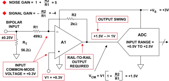
The input range of the ADC in Figure 6.12 is now +0.5 V to +2.5 V, and the entire circuit must operate on a +3-V power supply. A rail-to-rail output op amp is therefore required for A1 in order to ensure adequate output signal swing. Note that in addition, the input common-mode voltage of A1 is now +0.3 V in order to set the output common-mode voltage of +1.5 V (noise gain = +5, signal gain = –4). In order to allow an input common-mode voltage of +0.3 V, A1 must have either a PNP or PMOS input stage or a rail-to-rail input stage as previously shown in Figure 6.7.
This simple example serves to illustrate the importance of carefully examining the input/output signal level requirements placed on the op amp by the circuit conditions and the ADC interface. After the amplifier signal level requirements are established, then ac performance should be determined.
+VS – + BIPOLAR INPUT R2 R1 ADC RT V1 = +1.25V VCM= V1 1 + R2R1 A1 A1 PROVIDES BUFFERING, GAIN (IF DESIRED),
AND LEVEL SHIFTING
= +5V 1kΩ 1kΩ ±1V = +2.5V 52.3Ω +2.5V – /+ 1V INPUT RANGE = +1.5V TO +3.5V NOISE GAIN = 1 + R2 R1 SIGNAL GAIN = – R2 R1
SOME NON RAIL-TO-RAIL SINGLE-SUPPLY OP AMPS MAY BE USED FOR A1
INPUT COMMON-MODE VOLTAGE = +1.25V OUTPUT SWING = 2 = –1
Figure 6.12: Single-Ended Level Shifter with Gain Requires Rail-to-Rail Op Amp
Op Amp AC Specifications and Data Converter Requirements
Modern op amps come with what may appear to be a relatively complete set of dc and ac specifications—however fully specifying an op amp under all possible circuit conditions is almost impossible. For example, Figure 6.13 shows some key specifications taken from the table of specifications on the datasheet for the AD8057/AD8058 high speed, low distortion op amp (Reference 2). Note that the specifications depend on the supply voltage, the signal level, output loading, etc. It should also be emphasized that it is customary to provide only typical ac specifications (as opposed to maximum and
minimum values) for most op amps. In addition, we have seen that there are restrictions
on the input and output common-mode signal ranges, which are especially important when operating on low voltage dual (or single) supplies.
Figure 6.13: AD8057/AD8058 Op Amp Key Specifications, G = +1
+VS – + BIPOLAR INPUT R2 R1 ADC RT V1 = +0.3V VCM= V1 1 + R2R1 A1 = +3V 499Ω 2kΩ ±0.25V = +1.5V 56.2Ω +1.5V – /+ 1V INPUT RANGE = +0.5V TO +2.5V NOISE GAIN = 1 + R2 R1 SIGNAL GAIN = – R2 R1 INPUT COMMON-MODE VOLTAGE = +0.3V OUTPUT SWING RAIL-TO-RAIL OUTPUT REQUIRED = 5 = –4
Input Common Mode Voltage Range Output Common Mode Voltage Range
Input Voltage Noise Small Signal Bandwidth
THD @ 5MHz, VO= 2V p-p, RL= 1kΩ THD @ 20MHz, VO= 2V p-p, RL= 1kΩ VS= ±5V VS= +5V –4.0V to +4.0V –4.0V to +4.0V 7nV/√Hz 325MHz – 85dBc – 62dBc +0.9V to +3.4V +0.9V to +4.1V 7nV/√Hz 300MHz – 75dBc – 54dBc SPECIFICATION
Most op amp datasheets contain a section that provides supplemental performance data for various other conditions not explicitly specified in the primary specification tables. For instance, Figure 6.14 shows the AD8057/AD8058 distortion as a function of
frequency for G = +1 and VS = ±5 V. Unless it is otherwise specified, the data represented
by these curves should be considered typical (it is usually marked as such).
Figure 6.14: AD8057/AD8058 Op Amp Distortion Versus Frequency G = +1, RL = 150 Ω, VS = ±5 V
Note however that the data in both Figure 6.14 (and also the following Figure 6.15) is given for a dc load of 150 Ω. This is a load presented to the op amp in the popular
application of driving a source and load-terminated 75-Ω cable. Distortion performance is generally better with lighter dc loads, such as 500 Ω to 1000 Ω (more typical of many ADC inputs), and this data may or may not be found on the datasheet.
On the other hand, Figure 6.15 shows distortion as a function of output signal level for a frequencies of 5 MHz and 20 MHz.
Whether or not specifications such as those just described are complete enough to select an op amp for an ADC driver application depends upon the ability to match op amp specifications to the actually required ADC operating conditions. In many cases, these comparisons will at least narrow the op amp selection process. The following sections will examine a number of specific driver circuit examples using various types of ADCs, ranging from high resolution measurement to high-speed, low distortion applications.
Figure 6.15: AD8057/AD8058 Op Amp Distortion Versus Output Voltage G = +1, RL = 150 Ω, VS = ±5 V
Driving High Resolution
Σ-∆Measurement ADCs
The AD77xx family of ADCs is optimized for high resolution (16–24 bits) low frequency transducer measurement applications. Details of operation for this family can be found in Reference 3, and general characteristics of the family are listed in Figure 6.16.
Figure 6.16: Characteristics of AD77xx-family High Resolution Σ-∆ Measurement ADCs
Some members of this family, such as the AD7730, have a high impedance input buffer which isolates the analog inputs from switching transients generated in the front-end programmable gain amplifier (PGA) and the Σ-∆ modulator. Therefore, no special
THD @
THD @
Resolution: 16 - 24 bits
Input signal bandwidth: <60Hz Effective sampling rate: <100Hz
Designed to interface directly to sensors (< 1 kΩ) such as bridges with no external buffer amplifier (e.g., AD77xx - series)
On-chip PGA and high resolution ADC eliminates the need for external amplifier
If buffer is used, it should be precision low noise (especially 1/f noise) OP1177
OP177 AD797
precautions are required in driving the analog inputs. Other members of the AD77xx family, however, either do not have the input buffer, or if one is included on-chip, it can be switched either in or out under program control. Bypassing the buffer offers a slight improvement in noise performance.
The equivalent input circuit of the AD77xx family without an input buffer is shown below in Figure 6.17. The input switch alternates between the 10-pF sampling capacitor and ground. The 7-kΩ internal resistance, RINT, is the on-resistance of the input
multiplexer. The switching frequency is dependent on the frequency of the input clock and also the internal PGA gain. If the converter is working to an accuracy of 20-bits, the 10-pF internal capacitor, CINT, must charge to 20-bit accuracy during the time the switch
connects the capacitor to the input. This interval is one-half the period of the switching signal (it has a 50% duty cycle). The input RC time constant due to the 7-kΩ resistor and the 10-pF sampling capacitor is 70 ns. If the charge is to achieve 20-bit accuracy, the capacitor must charge for at least 14 time constants, or 980 ns. Any external resistance in series with the input will increase this time constant.
Figure 6.17: Driving Unbuffered AD77xx-Series Σ-∆ ADC Inputs
There are tables on the datasheets for the various AD77xx ADCs, which give the
maximum allowable values of REXT in order to maintain a given level of accuracy. These
tables should be consulted if the external source resistance is more than a few kΩ. Note that for instances where an external op amp buffer is found to be required with this type of converter, guidelines exist for best overall performance. This amplifier should be a precision low-noise bipolar-input type, such as the OP1177, OP177, or the AD797.
HIGH IMPEDANCE
> 1GΩ
SWITCHING FREQ
DEPENDS ON fCLKINAND GAIN
CINT 10pF TYP REXT RINT 7kΩ
~
REXTIncreases CINTCharge Time and May Result in Gain Error Charge Time Dependent on the Input Sampling Rate and Internal PGA Gain Setting
Refer to Specific Data Sheet for Allowable Values of REXTto Maintain Desired Accuracy
Some AD77xx-Series ADCs Have Internal Buffering Which Isolates Input from Switching Circuits
AD77xx-Series
(WITHOUT BUFFER) VSOURCE
Driving Single-Ended Input Single-Supply 1.6-V to 3.6-V Successive
Approximation ADCs
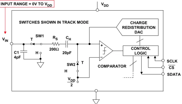
The need for low power, low supply voltage ADCs in small packages led to the development of the AD7466/AD7467/AD7468 12-/10-/ and 8-bit family of converters (Reference 4). These devices operate on supply voltages from 1.6 V to 3.6 V and utilize a successive approximation architecture which allows sampling rates up to 200 kSPS. The converters are packaged in a 6-lead SOT-23 package and offer this performance at only 0.62 mW with a 3-V supply and 0.12 mW with a 1.6-V supply. An automatic power-down mode reduces the supply current to 8 nA. Data is transferred via a simple serial interface. It is useful to examine these converters in more detail, because they illustrate some of the tradeoffs which must be made in designing appropriate interface circuits. A simplified block diagram of the series is shown in Figure 6.18. As mentioned, the ADC utilizes a standard successive approximation architecture based on a switched capacitor CMOS charge redistribution DAC. The input CMOS switches, SW1 and SW2, comprise the sample-and-hold function, and are shown in the track mode in the diagram. Capacitor C1 represents the equivalent parasitic input capacitance, CH is the hold capacitor, and RS
is the equivalent on-resistance of SW2. In the track mode, SW1 is connected to the input, and SW2 is closed. In this condition, the comparator is balanced, and the hold capacitor CH is charged to the value of the input signal. Assertion of the CS (convert start) starts
the conversion process: SW2 opens, and SW1 is connected to ground, causing the comparator to become unbalanced. The control logic and the charge redistribution DAC are used to add and subtract fixed amounts of charge from the hold capacitor to bring the comparator back into balance. At the end of the appropriate number of clock pulses, the conversion is complete.
Figure 6.18: Input Circuit of AD7466 1.6-V to 3.6-V, 12-Bit, 200-kSPS SOT-23-6 ADC
T H T H CONTROL LOGIC CHARGE REDISTRIBUTION DAC VDD 2 + – C1 4pF RS 200Ω CH 20pF COMPARATOR SW1 SW2 VIN
SWITCHES SHOWN IN TRACK MODE
VDD INPUT RANGE = 0V TO VDD
SCLK SDATA
The switching action of CMOS switches SW1 and SW2 places certain requirements on the input drive circuit with respect to the transient currents. In addition, the input signal must charge and discharge CH in the track mode. In most cases, no input drive amplifier
is required provided the source impedance is less than 1 kΩ (although a slight degradation in THD will be observed at input frequencies approaching 100 kHz). The input voltage range of the AD746x ADC is from 0 V to the supply voltage, and the supply also acts as the reference. If more accuracy or stability is required, the supply voltage can be derived from a voltage reference or an LDO.
Although single-supply rail-to-rail 1.8-V op amps are available (such as the AD8515, AD8517, and AD8631), these op amps will not drive signals completely to either rail due to the saturation voltage of the output transistors (this has previously been discussed in detail). If these are used as drive amplifiers to the AD746x, the usable input range of the ADC will be reduced by an amount which depends not only on this saturation voltage but the amount of additional headroom required at the amplifier output in order to give acceptable distortion performance at the higher input frequencies.
The overall conclusion of this discussion is that low voltage single-supply ADCs such as the AD746x are best driven directly from low impedance sources (< 1 kΩ). If a drive amplifier is required, it must operate on a higher supply voltage in order to utilize the full input range of the ADC.
Driving Single-Supply ADCs with Scaled Inputs
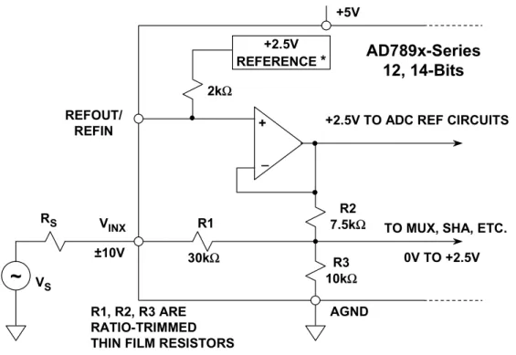
Even with the widespread popularity of single-supply systems, there are still applications where it is desirable for the ADC to process bipolar input signals. This can be handled in a number of ways, but a simple method is to provide an appropriate thin-film resistive divider/level-shifter at the input of the ADC. The AD789x and AD76xx family of single supply SAR ADCs (as well as the AD974, AD976, and AD977) include such a thin film resistive attenuator and level shifter on the analog input to allow a variety of input range options, both bipolar and unipolar.
A simplified diagram of the input circuit of the AD7890-10 12-bit, 8-channel ADC is shown in Figure 6.19 (Reference 5). This arrangement allows the converter to digitize a
±10-V input while operating on a single +5-V supply.
Within the ADC, the R1/R2/R3 thin film network provides attenuation and level shifting to convert the ±10-V input to a 0-V to +2.5-V signal that is digitized. This type of input requires no special drive circuitry, because R1 isolates the input from the actual converter circuitry that may generate transient currents due to the conversion process. Nevertheless, the external source resistance RS should be kept reasonably low, to prevent gain errors
Figure 6.19: Driving Single-Supply Data Acquisition ADCs With Scaled Inputs
Driving Differential Input CMOS Switched Capacitor ADCs
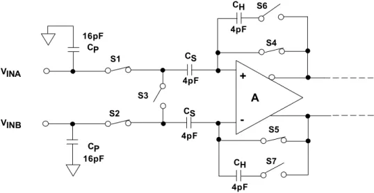
CMOS ADCs are quite popular because of their low power, high performance, and low cost. The equivalent input circuit of a typical CMOS ADC using a differential sample-and-hold is shown in Figure 6.20. While the switches are shown in the track mode, note that they open/close at the sampling frequency. The 16-pF capacitors represent the effective capacitance of switches S1 and S2, plus the stray input capacitance. The CS
capacitors (4 pF) are the sampling capacitors, and the CH capacitors are the hold
capacitors. Although the input circuit is completely differential, this ADC structure can be driven either single-ended or differentially. Optimum performance, however, is generally obtained using a differential transformer or differential op amp drive.
In the track mode, the differential input voltage is applied to the CS capacitors. When the
circuit enters the hold mode, the voltage across the sampling capacitors is transferred to the CH hold capacitors and buffered by the amplifier A (the switches are controlled by the
appropriate sampling clock phases). When the SHA returns to the track mode, the input source must charge or discharge the voltage stored on CS to the new input voltage. This
action of charging and discharging CS, averaged over a period of time and for a given fs
sampling frequency, makes the input impedance appear to have a benign resistive component. However, if this action is analyzed within a sampling period (1/fs), the input impedance is dynamic, and certain input drive source precautions should be observed.
+2.5V REFERENCE * + _
~
REFOUT/ REFIN VINX AGND RS 2kΩ R2 7.5kΩ R3 10kΩ 30kΩ+2.5V TO ADC REF CIRCUITS
TO MUX, SHA, ETC.
±10V 0V TO +2.5V AD789x-Series 12, 14-Bits VS R1 R1, R2, R3 ARE RATIO-TRIMMED THIN FILM RESISTORS
Figure 6.20: Simplified Input Circuit for a Typical Switched Capacitor CMOS Sample-and-Hold
The resistive component of the input impedance can be computed by calculating the average charge that is drawn by CH from the input drive source. It can be shown that if CS
is allowed to fully charge to the input voltage before switches S1 and S2 are opened that the average current into the input is the same as if there were a resistor equal to 1/(CSfS)
connected between the inputs. Since CS is only a few picofarads, this resistive component
is typically greater than several kΩ for an fS = 10 MSPS.
Over a sampling period, the SHA's input impedance appears as a dynamic load. When the SHA returns to the track mode, the input source should ideally provide the charging current through the RON of switches S1 and S2 in an exponential manner. The
requirement of exponential charging means that the source impedance should be both low and resistive up to and beyond the sampling frequency.
A differential input CMOS ADC can be driven single-ended with some ac performance degradation. An important consideration in CMOS ADC applications are the input switching transients previously discussed. Typical single-ended transients for a CMOS ADC are shown in Figure 6.21 for the AD9225 12-bit, 25-MSPS ADC. This data was taken driving the ADC with an equivalent 50-Ω source impedance. During the sample-to-hold transition, the input signal is sampled when CS is disconnected from the source.
Notice that during the hold-to-sample transition, CS is reconnected to the source for
recharging. The transients consist of linear, nonlinear, and common-mode components at the sample rate.
VINB
+
-SWITCHES SHOWN IN TRACK MODE A VINA CP 16pF CP 16pF S1 S2 S3 S4 S5 S7 S6 CS 4pF CS 4pF CH 4pF CH 4pF
Figure 6.21: Single-Ended Input Transients for a Typical CMOS ADC Sampling at 25 MSPS
Single-Ended Drive Circuits for Differential Input CMOS ADCs
A few simple single-ended drive circuits suitable for CMOS ADCs will now be
examined. Although differential drive is preferable for best ac performance, single-ended drivers are often adequate in less demanding applications.
Figure 6.22 shows a generalized single-ended op amp driver for a CMOS ADC. In this circuit, series resistor RS has a dual purpose. Typically chosen in the range of 25-100 Ω,
it limits the peak transient current from the driving op amp. Importantly, it also decouples the driver from the ADC input capacitance (and possible phase margin loss).
Figure 6.22: Optimizing a Single-Ended Switched Capacitor ADC Input Drive Circuit
Hold-to-Sample Mode Transition
Sample-to-Hold Mode Transition
Hold-to-Sample Mode Transition- CSReturned to Source for "recharging". Transient Consists of Linear, Nonlinear, and Common-Mode Components at Sample Rate .
Sample-to-Hold Mode Transition- Input Signal Sampled when CSis disconnected from Source.
Note: Data Taken with 50Ω
Source Resistance VINA VINB VREF AD92xx + – RS RS CF CF 10µF 0.1µF VIN
Another feature of the circuit are the dual networks of RS and CF. Matching both the dc
and ac source impedance for the ADC's VINA and VINB inputs ensures symmetrical settling
of common-mode transients, for optimum noise and distortion performance. At both inputs, the CF shunt capacitor also acts as a charge reservoir and steers the common-mode
transients to ground.
In addition to the buffering of transients, RS and CF also form a lowpass filter for VIN,
which limits the output noise of the drive amplifier into the ADC input VINA. The exact
values for RS and CF are generally optimized within the circuit, and the recommended
values given on the ADC datasheet.
Many important factors should be considered in selecting an appropriate drive amplifier. As discussed previously, common-mode input and output voltages must be compatible with the ADC power supply and input range. The op amp noise and distortion
performance should be compatible with the expected performance of the ADC. In addition, the settling time of the op amp should be fast enough so that the output can settle from the transient currents produced by the ADC. A good guideline is that the 0.1% settling time of the op amp should be no more than one-half the period of the maximum sampling frequency. The most important factor is simply to consult the ADC data sheet for recommended drive op amps and the associated circuits.
A generalized dc-coupled single-ended op amp driver and level shifter for the AD922x-series of ADCs is shown in Figure 6.23. The values in this circuit are suitable for sampling rates up to about 25 MSPS. This circuit interfaces a ±2-V ground-referenced input signal to the single-supply ADC, and also provides transient current isolation. The ADC input voltage range is 0 to +4-V, and a dual supply op amp is required, since the ADC minimum input is 0 V.
Figure 6.23: Single-Ended DC-Coupled Level Shifter and Driver for the AD922x ADC 52.3Ω +5V VINA VINB + -AD8057 +5V 1kΩ 0.1µF 0.1µF 1kΩ 1kΩ 1kΩ 1kΩ 10µF 0.1µF + –5V VREF 100pF 100pF INPUT ±2V +1.0V +2.0V – /+2V +2.0V AD922x 33.2Ω 33.2Ω
INPUT RANGE SET FOR 0V to +4V
The non-inverting input of the AD8057 is biased at +1 V, which sets the output common-mode voltage at VINA to +2 V for a bipolar input signal source. Note that the VINA and
VINB source impedances are matched for better common-mode transient cancellation. The
100-pF capacitors act as small charge reservoirs for the input transient currents, and also form lowpass noise filters with the 33.2-Ω series resistors.
A similar single-ended level shifter and driver is shown in Figure 6.24, however this circuit is designed to operate on a single +5-V supply. In this circuit the bipolar ±1-V input signal is interfaced to the input of the ADC whose range is set for 2 V about a +2.5-V common-mode voltage. The AD8061 rail-to-rail output op amp is used, although others are suitable depending upon bandwidth and distortion requirements (for example, the AD8027, AD8031, or AD8091). The +1.25-V input common-mode voltage for the AD8061 is developed by a voltage divider from the external AD780 2.5-V reference.
Figure 6.24: Single-Ended DC-Coupled Single-Supply Level Shifter for Driving AD922x ADC
Differential Input ADC Drivers
As previously discussed, most high performance ADCs are now being designed with differential inputs. A fully differential ADC design offers the advantages of good common-mode rejection, reduction in second-order distortion products, and simplified factory trimming algorithms. Although most differential input ADCs can be driven single-ended as previously described, a fully differential driver usually optimizes overall performance.
In the following discussions, it is useful to keep in mind that there are currently two popular IC processes used for high performance ADCs, and each one has certain application implications. Many medium-to-high performance ADCs are fabricated on high density foundry CMOS processes, and these typically use switched capacitor
10µF +5V 52.3Ω INPUT + +5V AD922x VINA VINB + -AD8061** +5V 0.1µF 1kΩ 0.1µF 1kΩ ADR431 2.5V REF. 1kΩ 1kΩ 10µF + 100pF 100pF ± 1V +2.5V – /+ 1V +1.25V +2.5V 33.2Ω 33.2Ω
**ALSO AD8027, AD8031, AD8091 (SEE TEXT)
INPUT RANGE SET FOR +1.5V to +3.5V
sample-and-hold techniques (previously described) which tend to generate transient currents at the ADC inputs. In many cases, however, ultra high performance ADCs are designed on either BiCMOS (bipolar and CMOS devices on the same process) or CB (complementary bipolar) processes. ADCs designed on BiCMOS or CB processes typically provide input buffers as part of a more conventional diode-switched sample-and-hold circuit which minimize the effects of input transient currents—however, the input range is generally less flexible than in CMOS-based designs.
In order to understand the advantages of common-mode rejection of input transient currents, we will next examine the waveforms at the two inputs of the AD9225 12-bit, 25-MSPS CMOS ADC as shown in Figure 6.25A, designated as VINA and VINB. The
balanced source impedance is 50 Ω, and the sampling frequency is set for 25 MSPS. The diagram clearly shows the switching transients due to the internal ADC switched
capacitor sample-and-hold. Figure 6-25B shows the difference between the two waveforms, VINA− VINB.
Figure 6.25: Typical Single-Ended (A) and Differential (B) Input Transients of CMOS Switched Capacitor ADC Sampling at 25 MSPS
Note that the resulting differential charge transients are symmetrical about mid-scale, and that there is a distinct linear component to them. This shows the reduction in the
common-mode transients, and also leads to better distortion performance than would be achievable with a single-ended input.
Transformer coupling into a differential input ADC provides excellent common-mode rejection and low distortion, provided performance to dc is not required. Figure 6.26 shows a typical circuit. The transformer is a Mini-Circuits RF transformer, model #ADT4-1WT which has an impedance ratio of 4 (turns ratio of 2). The 3-dB bandwidth of this transformer is 2 MHz to 775 MHz (Reference 6). The schematic assumes that the signal source impedance is 50 Ω. The 1:4 impedance ratio requires the 200-Ω secondary termination for optimum power transfer and low VSWR. The center tap of the
VINA
VINB
VINA-VINB
(A) (B)
Differential charge transient is symmetrical around mid-scale and dominated by linear component
Common-mode transients cancel with equal source impedance
transformer secondary winding provides a convenient means of level shifting the input signal to the optimum VC/2 common-mode voltage of the ADC (some ADCs may have a
common-mode voltage different than VC/2, so the data sheet should be consulted).
Figure 6.26: Transformer Coupling into a Differential Input CMOS ADC Transformers with other turns ratios may also be selected to optimize the performance for a given application. For example, a given input signal source or amplifier may realize an improvement in distortion performance at reduced output power levels and signal swings. Hence, selecting a transformer with a higher impedance ratio effectively "steps up" the signal level thus reducing the driving requirements of the signal source.
The network consisting of RS, C1, and C2 is relatively common when driving CMOS
switched capacitor ADC inputs with a transformer. The RS resistors serve to isolate the
transformer secondary winding from the switching transients, and the optimum value (determined empirically) generally ranges from 25 to 100 Ω. The C1 capacitors serve as common-mode charge reservoirs for the switching transients and also provide noise filtering (in conjunction with the RS resistors). The C1 capacitors should have no greater
than 5% tolerance to prevent common-mode to differential signal conversion. If needed, C2 can be added for additional differential filtering. Data sheets for most CMOS ADCs typically recommend optimum values for RS, C1, and C2 and should be consulted in all
cases.
As previously mentioned, BiCMOS or complementary bipolar ADCs typically provide some amount of input buffering, and therefore have lower input transient currents than CMOS converters. Figure 6.27 shows two typical input configurations for buffered BiCMOS or CB ADCs. Although this can simplify the interface, the fixed input
common-mode level may limit flexibility. In Figure 6.27A the common-mode voltage is developed with a resistive divider connected between ground and the positive analog supply voltage. In Figure 6.27B, the common-mode voltage is generated by an internal reference voltage. +VC AD92xx VIN+ VIN– 0.1µF 200Ω 1Vp-p 1:2 Turns Ratio 1:4 Impedance Ratio RF TRANSFORMER: MINI-CIRCUITS ADT4-1WT 1kΩ 1kΩ HIGH INPUT Z CMOS ADC C1 C1 C2 RS RS VCM 50Ω
Figure 6.27: ADCs with Buffered Differential Inputs (BiCMOS or Complementary Bipolar Process)
Figure 6.28 shows a transformer drive circuit for the AD9430 12-bit, 170-/210-MSPS BiCMOS ADC (Reference 7). For best performance at high input frequencies, two transformers are connected in series as shown to minimize even-order harmonic
distortion. The first transformer converts the single-ended signal to a differential signal— however the grounded input on the primary side degrades the amplitude balance on the secondary winding because of the stray capacitive coupling between the windings. The second transformer improves the amplitude balance, and thus the harmonic distortion. A wideband transformer, such as the Mini Circuits ADT1-1WT is recommended for these applications. The 3-dB bandwidth of the ADT1-1WT is 0.4 MHz to 800 MHz. Note that the bandwidth through the two transformers is equal to the bandwidth of a single
transformer divided by √2.
The net impedance seen by the secondary winding of the second transformer is the sum of the ADC input impedance (6 kΩ) and the two 24.9-Ω series resistors, or approximately 6050 Ω. The 51.1-Ω termination resistor in parallel with 6050 Ω yields the desired
impedance of approximately 50 Ω.
There is no requirement for input filtering, since the BiCMOS buffered input circuit generates minimal transient currents. The 24.9-Ω series resistors simply buffers the transformer from the small input capacitance of the ADC (~5 pF). The input common-mode voltage is set at +2.8 V by the 3.5-kΩ/20-kΩ resistive divider (when operating on a +3.3-V supply). This serves to illustrate the point made earlier that BiCMOS and
complementary bipolar ADCs may not have a common-mode voltage that is exactly mid-supply. In this circuit, the most positive input voltage on either input is 2.8 V + 0.384 V = 3.184 V which is only 116 mV from the +3.3-V supply. The implication therefore is that for low distortion performance in a 3.3-V system, the AD9430 must either be driven from a transformer or from an ac-coupled differential amplifier.
GND AVDD VINB R1 R1 R2 R2 INPUT BUFFER SHA
VINA BUFFERINPUT SHA
VREF VINA
VINB
Input buffers typical on BiCMOS and bipolar processes Difficult on CMOS
Simplified input interface - low transient currents Fixed common-mode level may limit flexibility
If dc coupling is required, the driving amplifier must operate on a higher supply voltage, because even rail-to-rail output stages will give poor high frequency distortion
performance if only 116-mV of headroom is available.
Figure 6.28: Transformer Coupling into the AD9430 12-Bit, 170-/210-MSPS BiCMOS ADC
Note that the center tap of the secondary winding of the transformer is decoupled to ground to ensure a balanced drive.
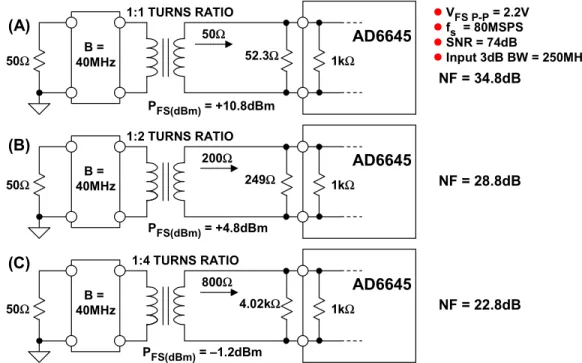
A similar transformer drive circuit for the AD6645 14-bit, 80-/105-MSPS (bipolar process) ADC is shown in Figure 6.29 (Reference 8). Note that the input common-mode voltage is developed by the two 500-Ω resistors connected to each input from the internal 2.4-V reference. The differential input resistance of the ADC is therefore 1 kΩ. As in the previous circuit, the 24.9-Ω series resistors isolate the transformer secondary winding from the small input capacitance of the ADC. The net differential impedance seen by the secondary winding of the transformer is therefore 1050 Ω.
In this circuit, a Mini Circuits ADT4-1WT 1:4 impedance ratio (1:2 turns ratio)
transformer is used to match the 1050-Ω differential resistance to the 50-Ω source. The 1050-Ω resistance is 262.5 Ω referred to the primary winding, and the 61.9-Ω
termination resistor in parallel with 262.5 Ω is approximately 50 Ω. The 3-dB bandwidth of the transformer is 2 MHz to 775 MHz. MINICIRCUITS ADT1-1WT +3.3V 0.1µF 3.5kΩ 3.5kΩ 20kΩ 20kΩ 24.9Ω 24.9Ω 3kΩ 3kΩ 51.1Ω 1:1 1:1 ±0.768V +2.8V +/– 0.384V +2.8V –/+ 0.384V AD9430
Theoretically, a 1:20 impedance ratio (corresponding to a 1 : 4.47 turns ratio) transformer would perfectly match the AD6645 1000-Ω input to the 50-Ω source and provide a "noise-free" voltage gain of 4.47 (+13 dB). However, this large turns ratio could result in unsatisfactory bandwidth and distortion performance.
Figure 6.29: Transformer Coupling into the AD6645 14-Bit, 80-/105-MSPS Complementary Bipolar Process ADC
To illustrate the effects of utilizing transformers for voltage gain on system noise figure (NF), Figure 6.30 shows the AD6645 sampling a 40-MHz bandwidth signal at 80 MSPS for turns ratios of 1:1 (Figure 6.30A), 1:2 (Figure 6.30B) and 1:4 (Figure 6.30C). (Refer back to Chapter 2 for the basic definitions and calculations of ADC noise figure).
Notice that each time the turns ratio is doubled, the noise figure decreases by 6 dB. In practice, however, empirical data indicates that bandwidth and distortion are
compromised when driving the AD6645 with a turns ratio of greater than 1:2.
MINICIRCUITS ADT4-1WT +5V 0.1µF 500Ω 500Ω 24.9Ω 24.9Ω 500Ω 500Ω 61.9Ω 1:2 TURNS RATIO ±0.58V +2.4V +/– 0.55V +2.4V –/+ 0.55V AD6645 VREF= +2.4V 1:4 IMPEDANCE RATIO
Figure 6.30: Using RF Transformers to Improve Overall ADC Noise Figure
Driving ADCs with Differential Amplifiers
Certainly for most RF and IF applications, transformer ADC drivers yield the best overall distortion and noise performance, especially if the transformer can be utilized to achieve some amount of "noise free" voltage gain. There are, however, many applications where differential input ADCs cannot be driven with transformers because the frequency response must extend to dc. In these cases, the op amp common-mode input and output voltage, gain, distortion, and noise must be carefully considered in designing dc-coupled drive circuitry. The following two subsections discuss two types of differential op amp drivers: the first is based on utilizing dual op amps, and the second utilizes fully integrated differential amplifiers.
Dual Op Amp Drivers
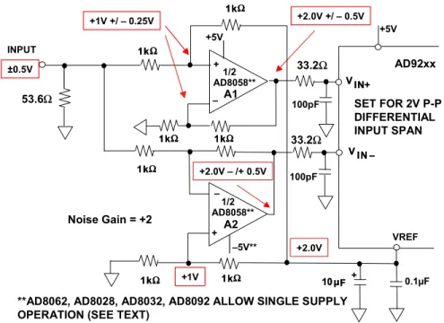
Figure 6.31 shows how the dual AD8058 op amp can be connected to convert a single-ended bipolar signal to a differential one suitable for driving the AD92xx family of CMOS ADCs. Utilizing a dual op amp provides better gain and phase matching than would be achieved by simply using two single op amps. The input range of the ADC is set for a 2-V p-p differential input signal (1-V p-p on each input), and a common-mode voltage of +2 V. As shown for previous CMOS ADCs, the 100-pF capacitors serve as charge reservoirs for the transient currents, and also act as lowpass noise filters in conjunction with the 33.2-Ω resistors.
The A1 amplifier is configured as a non-inverting op amp. The 1-kΩ divider resistors level shift the ±0.5-V input signal to +1 V ±0.25 V at the non-inverting input of A1. The output of A1 is therefore +2 V +/–0.5 V, because the non-inverting gain of A1 is 2.
50Ω 52.3Ω 1kΩ 1:1 TURNS RATIO AD6645 50Ω 249Ω 1kΩ 1:2 TURNS RATIO AD6645 200Ω 4.02kΩ 1kΩ 1:4 TURNS RATIO AD6645 800Ω NF = 34.8dB NF = 28.8dB NF = 22.8dB PFS(dBm)= +10.8dBm PFS(dBm)= +4.8dBm PFS(dBm)= –1.2dBm (A) (B) (C) VFS P-P= 2.2V fs = 80MSPS SNR = 74dB Input 3dB BW = 250MHz B = 40MHz 50Ω 40MHzB = 50Ω 40MHzB =
Figure 6.31: Op Amp Single-Ended to Differential DC-Coupled Driver with Level Shifting
The A2 op amp inverts the input signal, and the 1-kΩ divider resistors establish a +1-V common-mode voltage on its non-inverting input. The output of A2 is therefore +2 V –/+0.5 V.
This circuit provides good matching between the two op amps because they are duals on the same die and are both operated at the same noise gain of 2. However, the input voltage noise of the AD8058 is 20 nV/√Hz, and this appears as 40 nV/√Hz at the output of both A1 and A2 thereby, introducing possible SNR degradation in some applications. In the circuit of Figure 6.31, this is mitigated somewhat by the input RC network which not only reduces the input noise, but also absorbs some of the transient currents.
The AD8058 op amp does not have rail-to-rail inputs or outputs, and the following simple analysis shows that the circuit as shown in Figure 6.31 must use dual supplies. The output common-mode voltage of the AD8058 operating on a single +5-V supply is +0.9 V to +3.4 V, which would be acceptable in this circuit, because the required signal swing is only +1.5 V to +2.5 V. However, the input common-mode voltage of the AD8058 operating on a single +5-V supply is specified as +0.9 V to +4.1 V; but the circuit requires that the input common-mode voltage go to +0.75 V, which is outside the allowable range. Therefore, a dual supply is required for the op amp.
If single supply operation is required, however, there are a number of dual rail-to-rail op amps which should be considered, such as the AD8062, AD8028, AD8032, and the AD8092. Noise Gain = +2 +5V V IN – V IN – V IN+ V IN+ + – AD8058** 10 µF 10 µF + 0.1µF 1kΩ 1kΩ VREF 100pF 100pF 1kΩ 1kΩ 1kΩ 1kΩ 1kΩ 1kΩ 1kΩ 1kΩ 1kΩ 1kΩ + – AD8058** +2.0V – /+ 0.5V +2.0V 1kΩ 1kΩ INPUT AD92xx +1V +/ – 0.25V SET FOR 2V P-P DIFFERENTIAL INPUT SPAN +5V –5V** A1 A2 1/2 1/2 ±0.5V +2.0V +/ – 0.5V +1V 53.6Ω 33.2Ω 33.2Ω
**AD8062, AD8028, AD8032, AD8092 ALLOW SINGLE SUPPLY OPERATION (SEE TEXT)
Fully Integrated Differential Amplifier Drivers
A block diagram of the AD813x family of fully differential amplifiers optimized for ADC driving is shown in Figure 6.32 (see Reference 9). Figure 6.32A shows the details of the internal circuit, and Figure 6.32B shows the equivalent circuit. The gain is set by the external resistors RF and RG, and the common-mode voltage is set by the voltage on
the VOCM pin. The internal common-mode feedback forces the VOUT+ and VOUT– outputs
to be balanced, i.e., the signals at the two outputs are always equal in amplitude but 180° out of phase per the equation,
VOCM = ( VOUT+ + V OUT– ) / 2. Eq. 6.4
The AD813x uses two feedback loops to separately control the differential and common-mode output voltages. The differential feedback, set with external resistors, controls only the differential output voltage. The mode feedback controls only the common-mode output voltage. This architecture makes it easy to arbitrarily set the output
common-mode level in level shifting applications. It is forced, by internal common-mode feedback, to be equal to the voltage applied to the VOCM input, without affecting the
differential output voltage. The result is nearly perfectly balanced differential outputs of identical amplitude and exactly 180° apart in phase over a wide frequency range. The circuit can be used with either a differential or a single-ended input, and the voltage gain is equal to the ratio of RF to RG.
Figure 6.32: AD813x Differential ADC Driver Functional Diagram and Equivalent Circuit
~ RF RF RG RG VOUT– VOUT+ + – GAIN = RF RG VIN+ VIN– EQUIVALENT CIRCUIT: VOCM + – + – – + + – RF RF RG RG VIN+ VIN– VOUT+ VOUT– VOCM V+ V– (A) (B)