ABSTRACT
Title of Document: Performance Analysis of
NAND Flash Memory Solid-State Disks
Cagdas Dirik
Doctor of Philosophy, 2009
Directed By: Professor Bruce Jacob
Department of Electrical and Computer Engineering University of Maryland, College Park
As their prices decline, their storage capacities increase, and their endurance improves, NAND Flash Solid-State Disks (SSD) provide an increasingly attractive alternative to Hard Disk Drives (HDD) for portable computing systems and PCs. HDDs have been an integral component of computing systems for several decades as long-term, non-volatile storage in memory hierarchy. Today’s typical hard disk drive is a highly complex electro-mechanical system which is a result of decades of research, development, and fine-tuned engineering. Compared to HDD, flash memory provides a simpler interface, one without the complexities of mechanical parts. On the other hand, today’s typical solid-state disk drive is still a complex storage system with its own peculiarities and system problems.
Due to lack of publicly available SSD models, we have developed our NAND flash SSD models and integrated them into DiskSim, which is extensively used in
academe in studying storage system architectures. With our flash memory simulator, we model various solid-state disk architectures for a typical portable computing
environment, quantify their performance under real user PC workloads and explore potential for further improvements. We find the following:
• The real limitation to NAND flash memory performance is not its low per-device bandwidth but its internal core interface.
• NAND flash memory media transfer rates do not need to scale up to those of HDDs for good performance.
• SSD organizations that exploit concurrency at both the system and device level improve performance significantly.
• These system- and device-level concurrency mechanisms are, to a significant degree, orthogonal: that is, the performance increase due to one does not come at the expense of the other, as each exploits a different facet of concurrency
exhibited within the PC workload.
• SSD performance can be further improved by implementing flash-oriented
queuing algorithms, access reordering, and bus ordering algorithms which exploit the flash memory interface and its timing differences between read and write requests.
PERFORMANCE ANALYSIS OF NAND FLASH MEMORY SOLID-STATE DISKS
by
Cagdas Dirik
Dissertation submitted to the Faculty of the Graduate School of the University of Maryland, College Park, in partial fulfillment
of the requirements for the degree of Doctor of Philosophy
2009
Advisory Committee:
Professor Bruce Jacob, Chair Professor Donald Yeung Professor Gang Qu
Professor Jeff Hollingsworth Professor Prakash Narayan
© Copyright by Cagdas Dirik
To my parents, Zehra and Engin Dirik
Acknowledgements
First, I would like to thank my advisor, Professor Bruce Jacob. This thesis would not have been possible without his guidance, support, and endless patience.
I had the privilege to be friends and work with many great people. Mustafa Tikir has always been there for me through good times and bad times. He always listened to my drama and shared his valuable thoughts. I am very grateful to him for all the things he has done. Professor Yavuz Oruc has been a great mentor to me. He provided his advice throughout my struggles and kept me challenged. Thanks to Okan Kolak, Murat Ungor, Nihal Bayraktar, Betul Atalay, Parag Kulkarni, Samuel Rodriguez, Hongxia Wang, Amol Gole, Akin Akturk, Aydin Balkan, Fusun Yaman, Evren Sirin, Burcu Karagol, Fazil Ayan, Yakup Bayram for their friendship and emotional support.
Special thanks to my wife, Allyson. She had to witness the last years of a PhD student and I am afraid this has irreversibly damaged her perception of graduate school. I am grateful for her endless love and support, without which I could not survive.
Foremost, I would like to thank to my mother and father for their love and
support. They have always been there for me, every step of my education. Long time ago they stopped asking me "when I will be graduating". This is the biggest relief for a graduate student. Thank you for believing in me.
Table of Contents
... Chapter 1: Introduction 1 ... 1.1. Problem Description 1 ...1.2. Contribution and Significance 5
...
1.3. Organization of Dissertation 8
...
Chapter 2: Overview of NAND Flash Memory 10
...
2.1. Non-Volatile Memory 10
...
2.2. Flash Memory Cell 13
...
2.3. NOR vs. NAND FLASH 14
...
2.4. Industry Trends 17
...
Chapter 3: NAND Flash Solid-State Disks 23
... 3.1. SSD vs. HDD: Cost, Performance and Power Comparison 23
...
3.2. Endurance: Reality or Myth? 27
...
3.3. SSD Organization 29
...
Chapter 4: Related Work 45
...
4.1. Flash Memory Simulations 45
...
4.2. Flash Memory Architectures and Performance 48
...
4.3. Hybrid Memory Systems 52
...
4.4. Flash Memory Data Structures and Algorithms 53
...
Chapter 5: Methodology 62
...
5.1. DiskSim Disk Simulator 62
...
5.2. NAND Flash Solid-State Disk Simulator 63
...
...
5.4. Simulation Parameters 72
...
Chapter 6: Experimental Results 82
...
6.1. Banking and Request Interleaving 82
...
6.2. Superblocks 97
...
6.3. Concurrency: Banking vs. Superblocks 103
...
6.4. Media Transfer Rate 113
...
6.5. System Bandwidth and Concurrency 118
...
6.6. Improving I/O Access 136
...
6.7. Request Scheduling 148
...
6.8. Block Cleaning 163
...
6.9. Random Writes and Mapping Granularity 175
...
Chapter 7: Conclusions and Future Work 181
...
Chapter 1: Introduction
1.1. Problem Description
Flash-based solid-state disks are rapidly becoming a popular alternative to hard disk drives as permanent storage, particularly in netbooks, notebooks and PCs, because of flash's faster read access, low power consumption, small size, shock resistance, and reliability compared to hard disks. SSDs are commercially available in numerous commodity PC models today; they are considered a high-end option due to price-per-bit that is higher than HDDs, but that price gap is closing very quickly.
Flash technology has additional characteristics that have slowed its takeover of hard disks, including a lower bit density relative to HDDs, limited endurance (i.e., its limited number of write cycles), and write performance. Solutions have reached a level of maturity to place flash on a near-term crossover with disks. Rapid migration to later technology has been driving the bit cost of NAND flash significantly lower and its density higher. NAND flash capacity has doubled every year since 2001 and is expected to continue at that rate until 2010; by 2010 it is expected to reach 32/64 Gb single chip density [39, 58, 74]. Over the same period, cost of NAND flash memory has decreased 40-50% per year [69]. In addition, technological enhancements and architectural mechanisms have improved flash memory endurance - currently, NAND flash from several vendors is commercially available with an endurance rating of more than 50 years at 50 GB write per day. Soon, the limit on the number of writes will become a fading memory.
Today’s typical hard disk drive is a highly complex electro-mechanical system which is a result of decades of research, development, and fine-tuned engineering. Despite this complexity, extremely detailed and accurate models of HDDs are publicly available [33]. Compared to HDD, flash memory provides a simpler interface, especially one without the complexities of mechanical parts. On the other hand, today’s typical solid-state disk drive is still a complex storage system with its own peculiarities and system problems. NAND flash solid-state disks employ multiple flash memory arrays in parallel to increase storage system bandwidth and performance. When multiple flash memory arrays are available, data placement becomes a critical problem for performance and load balancing. Flash memory programming rate is considerably slow and in-place update of data is not allowed. Asymmetric read and write rates make solid-state disk performance more dependent on user workload. Effective wear leveling and block cleaning are two other issues unique to flash memory systems. As it is stated by Agrawal et. at., issues that arise in flash memory solid-state disk design mimic complex system problems that normally appear higher in the storage stack, or even in distributed systems [1].
The relationship between flash memory system organization and its performance is both complex and very significant [1, 40, 24]. Very little has been published on the internals of solid-state disk drives; even less has been published on the performance resulting from various flash memory design options. The most in-depth study to date has been by Agrawal et. al. [1], who analyzed different mapping and ganging/striping policies at the device level (i.e., assuming a flash device exported multiple array-select lines to
enable concurrent access within the device) and ganging at the system level, targeting both enterprise workloads and synthetic workloads. In this dissertation we study the full design space of system-level organization choices for solid-state disks, investigate device-level design trade-offs, and provide a model on how SSDs work. We address the following issues:
• Concurrency: By system-level organization we mean the design of the SSD, treating the individual flash devices as constants. Variables in this space include the number of independent busses, their organizations (widths, speeds, etc.), banking strategies, and management heuristics that connect the SSD’s flash controller to the flash devices. As shown by Agrawal et al., increasing the level of concurrency in the flash SSD system by striping across the planes within the flash device can amortize the write overhead and increase throughput significantly [1]. Concurrency has been shown in the HDD space to provide tremendous bandwidth increases in interleaved organizations (e.g. RAID). Flash is interesting because unlike disks, its form factor need not change when accommodating interleaved organizations: one can achieve significant levels of concurrency in an SSD without significantly changing its overall size and shape. We investigate the effects of concurrent access to different flash banks via the same channel or by replicating resources and providing multiple independent channels to different flash banks, or by a combination of two.
• Bandwidth issues: Common wisdom holds that SSD performance is limited by its media transfer rate. Currently, access to a single flash memory chip is provided by
an 8-bit bus which limits the available bandwidth to 33 MB/s (30 ns bus speed is common) for read access. For write requests, single chip bandwidth can be much lower at 6-10 MB/s due to slow programming time (200 µs for programming 2KB page). As interface transfer rates increase with the introduction of serial I/O interfaces and fiber channel, HDD performance will continue to scale, but SSD performance is expected to be limited by the device’s media transfer rate. Samsung's solution to this problem has been to move to a wider and higher performance bus, which can sustain 108 MB/s (16 bit, 54 MHz). Other vendors have followed suit. Two to three years ago, an 8-bit bus clocked at 50 ns was typical, whereas today most flash solid-state disks come with clocks speeds of 20– 30 ns. There is also a push by other vendors to improve read/write performance of flash disks by access via 800 MB/s bus in a ring topology [37].
• Write performance: Another approach to improving flash performance is to reduce the programming time, thus improving the throughput of write requests. For example, Micron proposed using two-plane flash devices which can
simultaneously read and program two pages (2 KBytes each) in the same flash die [59]. This effectively doubles sustainable read and write bandwidth (reported page program performance increases from 8.87 MB/s to 17.64 MB/s). Another
approach taken by Micron is combining flash memory blocks into so-called superblocks, enabling the simultaneous read or write of 2 or 4 pages within a flash device or even across different flash dies [57]. This mechanism is similar to Agrawal’s ganging and striping mechanisms. Samsung supports similar
architecture to hide programming latency wherein the flash controller controls 2 separate channels and supports 4-way interleaving (write throughput of 30 MB/s is reported) [64, 69].
In this dissertation we address the question; which of these issues is the most significant - i.e., what approaches to improving solid-state disk drive performance provide the best performance at the lowest cost? We model various flash solid-state disk architectures for a typical portable computing environment and quantify their performance under diverse user applications such as browsing, listening to music, watching videos, editing pictures, editing text and document creation, office application, and email applications. This dissertation also explores the potential for improvements to SSD organizations by flash oriented heuristics and policies. We study flash oriented queuing algorithms, access reordering, and bus ordering algorithms to accommodate asymmetric nature of read and write requests. We also address the question; how to optimize the internal I/O access to SSD storage system without significant changes to its physical organization?
1.2. Contribution and Significance
The contributions of this dissertation are three-fold:
1) We develop a solid-state disk simulator which can be used to measure performance of various NAND flash memory architectures. Our SSD simulator is designed as an extension to DiskSim v2.0 and models a generalized NAND flash solid-state disk by implementing flash specific read, program, erase commands, block cleaning and logical-to-physical address mapping, all while providing the illusion of an HDD. Our simulator is highly configurable and can simulate various solid-state disk architectures
while maintaining a view of a single disk drive to host system. We have used our own disk traces collected from portable computers and PCs running real user workloads to drive the SSD simulator. Our workloads represent typical multi-tasking user activity, which includes browsing files and folders, emailing, text editing and document creation, surfing the web, listening to music and playing movies, editing pictures, and running office applications. These workloads consist of not only I/O traffic generated by user applications, but also I/O read and write requests generated by system and admin processes [24].
2) We study NAND flash SSD architectures and their management techniques, quantifying SSD performance as a function of bandwidth, concurrency, device
architecture, and system organization. We explore full design space of system-level organization choices for solid-state disks. Variables in this space include number of flash memory chips, number of independent busses, their organizations (widths, speeds, etc.), banking strategies, and management heuristics that connect the SSD's flash controller to the flash devices. We also investigate device-level design trade-offs as well, including pin bandwidth and I/O width [24]. We find the following:
• The flash memory bus does not need to scale up to HDD I/O speeds for good performance. Average read response times, a good indicator of system-level CPI [40, p. 52], do not improve much beyond 100 MB/s bus bandwidth.
• The real limitation to flash memory performance is not its bus speed but its core interface: the movement of data between the flash device's internal storage array and internal 2 KB data and cache registers.
• SSD organizations that exploit concurrency at both the system and device level (e.g. RAID-like organizations and Micron-style superblocks) improve
performance significantly.
• These system- and device-level concurrency mechanisms are, to a significant degree, orthogonal: that is, the performance increase due to one does not come at the expense of the other, as each exploits a different facet of concurrency
exhibited within the PC workload.
• NAND flash interface provides drastically different read and write timing which results in large performance disparities between reads and writes. Increasing the level of concurrency in SSD systems amortizes write overhead and increases write throughput significantly. However, asymmetry between reads and writes and the scale factor between their performance persists.
3) We explore the potential for further improvements to SSD organizations by flash oriented heuristics and policies. When distinctive differences between reading from and writing to flash memory and the impact of system- and device-level concurrency techniques are taken into account, there is potential for exploiting the performance disparity between reads and writes. We study flash oriented queueing algorithms, access reordering, and bus ordering algorithms to accommodate asymmetric reads and writes. Specifically:
• Request scheduling heuristics: Most disk-scheduling algorithms attempt to reduce seek time, since the majority of time spent in servicing an I/O request in
solid-state disks do not have any mechanical components and therefore have a
deterministic, uniform request service time. We show that; even with this limited potential, one can improve SSD storage system performance significantly by implementing flash-specific request-scheduling algorithms that exploit the flash memory interface and its timing differences between read and write requests. • I/O bus access policies: We show that for a typical SSD physical organization
(which provides concurrent access to different flash memory banks via the same I/O channel or multiple independent channels to different flash banks, or by a combination of the two), timing of I/O access requests and bus utilization is an important factor in performance. By taking into account the differences between read and write timing and using different I/O access policies, I/O bus utilization can be improved considerably.
• Data burst size: With a significant level of request interleaving, I/O bus utilization becomes critical, especially for read requests. By increasing the burst size in transferring data from/to the flash memory array, the number of I/O access requests can be reduced, thereby reducing I/O bus congestion.
1.3. Organization of Dissertation
The dissertation is organized as follows: Chapter 2 provides an overview of NAND flash memory. Characteristics of NAND flash memory is summarized and compared against other types of flash memory. Details of NAND flash memory solid-state disk
architectures, including flash memory array organization, NAND flash interface, and flash specific algorithms, are covered in Chapter 3. Chapter 4 discusses related works for
the dissertation. Chapter 5 presents the methodology followed in the dissertation. Details of the SSD simulator designed and parameters for the simulations performed are also covered in chapter 5. Chapter 6 discusses the experimental results, mainly on the
performance of NAND flash memory solid-state disks. Chapter 7 provides the conclusion to the dissertation.
Chapter 2: Overview of NAND Flash Memory
Flash memory is a type of electrically erasable programmable read only memory (EEROM) invented by Dr. Fujio Masuoka in the 1980s while working at Toshiba. Main characteristics of flash memory, which differentiate it from other types of EEPROM, are its ability to program in large blocks and its low cost per bit. NAND type flash memory was first introduced by Toshiba in the late 1980s, following NOR type flash memory by Intel [63]. Although other types of flash memory have been developed, NAND and NOR types are the two dominant ones in volume production. Starting from mid 1990s
development of battery operated portable electronic appliances, such as PDAs and mobile phones, dramatically increased the popularity of flash memory and its market share. Driven by personal computer market and portable communications systems, flash memory will continue rise in popularity.
2.1. Non-Volatile Memory
Semiconductor memories can be grouped in two categories: volatile and non-volatile. Content of volatile memory (e.g., Random Access Memory) can be changed fast, easy, and unlimited number of times, but it is lost when the power is switched off. On the other hand, non-volatile memory (e.g., Read Only Memory and flash memory) can retain its content even when it is not powered. Early designs of non-volatile semiconductor memory were fabricated with permanent data and did not provide the ability to modify data content. Current designs can be erased and re-programmed a number of times although at a comparatively slow speed compared to RAM [12].
The very first non-volatile ROM was the mask-programmed ROM which was programmed during fabrication and could not be changed. Then in 1956, PROM was invented. PROM allowed engineers to program its content by using silicon or metal fuses. These fuses could be blown by a programmer to change the state of a memory cell from 0 to 1 exactly once. In the early 1970s EPROM was invented, which can be erased by exposure to ultraviolet light and programmed by applying high voltage. EPROM uses one transistor memory cell, thus it is a high density and low cost non-volatile memory. For example, early PC designs employed EPROM as their BIOS chip. In the 1980s EEPROM (Electrically erasable programmable ROM) introduced electrical erase capacity at byte granularity. Although a single byte could not be rewritten an unlimited number of times as in RAM, EEPROM provides good endurance - typically over 1 million program/erase cycle. However, EEPROM uses two transistors per memory cell and cell size cannot be easily scaled, therefore it is expensive and its density is much lower. Usually EEPROM has been used for storing parameters, user data, and
configuration settings of a device. Flash memory provides a good compromise between EPROM and EEPROM. Its single transistor per cell architecture provides low cost per bit and high density comparable to EPROM. At the same time its ability to erase and
program in large blocks provides flexibility comparable to EEPROM. Due to these characteristics, flash memory can be used both as code and user data storage and it has been successful in delivering to increasing demand for permanent storage driven by personal computer market and portable communications systems [12]. Figure 2.1 provides a comparison of various non-volatile memories.
Since the introduction of flash memory, many different flash technologies have been proposed. Among these, 4 types of flash memory have been adopted by industry: NOR type, divided bit line NOR (DINOR) type, NAND type, and AND type flash memory. Figure 2.2 shows a historical development of various flash memory
technologies. Out of these four types of flash memory, NOR and NAND flash have been dominant in volume production and the most widely used among industry - NOR and NAND flash can be considered as the industry standard. DINOR type flash memory was introduced by Mitsubishi and AND type was introduced by Hitachi [12, 11]. NOR flash is mostly utilized as code and parameter storage in embedded systems due to is high speed random access, and ability to program at byte level. NAND flash is usually used for data storage in memory cards due to its high speed programming and high speed serial access [12]. Most recently, NAND flash solid-state disks (SSDs) are becoming popular as hard disk drive (HDD) replacements in the mobile personal computer market.
pro Fit
TRIAL
version
ROM
EPROM
1T / cell Programmable and
electrically erasable Cost
Flexibility
FLASH Programmable and
erasable in system EEPROM
1T / cell
2T / cell Byte rewrite
capability
Not electrically programmable
Figure 2.1: Comparison of non-volatile memories. Flash memory provides a good compromise between EPROM and EEPROM and can be used both as code and user data storage. Figure adopted from [12, 5].
2.2. Flash Memory Cell
Flash memory cell is a single transistor cell using a dual gate MOS device. A floating gate exists between the control gate and silicon substrate. Floating gate is completely isolated by dielectrics, therefore can trap electrons and keep its charge [5].
For programming memory cell, NOR flash uses channel-hot-electron (CHE) injection while NAND flash uses Fowler-Nordheim (FN) tunneling. With the CHE injection method, MOSFET is properly biased in drain and gate and a large current flows into the cell. Due to this large current, electrons in the channel gain sufficient energy to overcome the gate oxide barrier and get trapped in the floating gate. In FN tunneling, only drain of MOS device is biased and less current is used for programming. Therefore programming by FN tunneling takes longer than CHE injection but allows many cells to
pro Fit TRIAL version `84 FLASH MEMORY Invention SanDisk-type `85 `86 `87 `91 NAND-type ACEE-type AND-type `92 NOR-type Split-gate-type SST-type `93 DINOR-type SanDisk-type NAND-type AND-type NOR-type SST-type DINOR-type x x File Storage Code Storage
Figure 2.2: History of flash memory technologies. NOR and NAND type have been
dominant flash memory types in volume production and the most widely used among industry. Figure adopted from [56].
be programmed simultaneously. Once electrons are trapped in the floating gate, they cannot escape high energy silicon dioxide barrier even after the device is powered off. When a flash memory cell is programmed, it is considered logic “0” because when it is read it cannot conduct a current due to increased threshold voltage by the trapped charges in the floating gate [11, 63, 5].
In both NAND and NOR flash, cell erasure is performed by FN tunneling. With negative biasing of the cell gate, a high electric field is formed across gate oxide helping trapped electrons to overcome the high energy barrier and depart the floating gate. When a flash memory cell is erased, it is considered storing logic “1” value [11, 63, 5].
2.3. NOR vs. NAND FLASH
In NOR flash memory, memory cells are connected in parallel with common ground node. NOR type array organization as shown in Figure 2.4. Bitlines are formed by memory cells sharing the same drain contact and wordlines are formed by flash cells
S D FG CG 10V Substrate 5V 0V S D FG CG 18V Substrate 0V 0V
CHE Injection FN Tunneling
S D FG CG -18V Substrate 5V 0V FN Tunneling
(a) Program (b) Erase
Figure 2.3: Flash memory programming and erase mechanisms. (a) In CHE injection, MOSFET is properly biased in drain and gate and electrons overcome the gate oxide barrier and get trapped in the floating gate. in FN tunneling, only drain of the MOS device is biased and less current is used. Once electrons are trapped in the floating gate, flash memory cell is programmed. (b) To erase flash memory cell, a high electric field is formed across gate oxide. This electric fields causes electrons to depart floating gate. Figure adopted from [78].
sharing gate contact. This array organization provides high speed direct access to a memory cell and high noise immunity - 100% guaranteed good bits [12, 5]. On the other hand, NAND flash memory employs a different array organization. In NAND flash, several memory cells are connected in series between bit line and ground, thus increasing the density compared to NOR flash - e.g., 4-5F2 NAND flash memory cell size vs. 9-10F2
memory cell size in NOR flash [63]. Actual sizes of two 64 MB flash memory dies are shown in figure 2.5 for comparison. Larger NOR flash memory cell size is due to bit line contact and ground contact for every two memory cells.
Although series connection of memory cells increases density in NAND flash, it reduces the current for read operation. Reading a single memory cell requires reading other cells in the same bit line, therefore NAND flash memory cannot provide fast random access and is usually employed as a serial memory. Moreover, reduced current in
Bit line Word line Source Bit line Word line Source Bit line sel.
Bit line sel.
(a) NOR array (b) NAND array
Figure 2.4: NOR and NAND flash memory array organizations. (a) In NOR flash memory, cells are connected in parallel. (b) In NAND flash, memory cells are connected in series resulting in increased density. Figure adopted from [12].
read operation makes NAND flash memory much more sensitive to noise and interference [12].
Fast random access time of NOR flash memory makes it ideal for code storage since the execution of code requires branching from one memory location to another. NOR flash memory can provide fully memory mapped random access interface with dedicated address and data lines, which also makes it better suited for code execution [5, 63]. Moreover, NOR flash memory is very reliable and guarantees 100% good bits. This eliminates the possibility of system faults and the need for error detection logic. On the other hand, NAND flash memory is used for data storage due to its serial access
characteristics. Also NAND flash memory provides higher storage density at a lower cost compared to NOR flash, which makes it better suited for data storage [5].
M-Systems 64 MBytes NAND
!
! ! "! #$%!#&'()%*%+,&-!.%/012&34!567!8-9!5:5;<!7&89!=9=! >=?@7?A=B?AC?"D! !"#$%&'(&)*+%&",-&.%,/*01(&.*/23,45*6&78&9/&:3;& ! "#$%&'()!*+,-$./')0!! 1/)23456/7!89!! *%:)(;!<4!$=5!>?>10! "#$%&'()!*+,-$./')0! $=5!>3@!AB:)6! ;,&! 0(%E%+210(! F-,G&!21E,%! /1,)E1,)&3H! !!!!!!!!!!! !!!!!!!!! ! ! !!!!!!!!!!! ! ;&)-,EI!J! =>KJ!L&EE&2!E(1)!567! ! ! ?'!:!CB:4D(E! 5:5;!,-!181,*1L*&!M2%/!=NOP!E%!Q=BOP! 567!,-!181,*1L*&!M2%/!=OP!E%!RBOP! NCOP!OD.!5:5;?L1-&3!;,-S6).(,0!,-!1L%TE!1!E(,23!%M!E(&!-,G&!! %M!&UT,81*&)E!NCOP!@E21E1!M*1-(!! 5:5;!,-!L&EE&2!02,'&3! 567!02%8,3&-!1!+%%3!-%*TE,%)!,)!*%$!'101',E,&-!M2%/!=OP!E%!COP!Q=BOL,E-V
BQNOL,E-BQNOL,E-!
! ! "! #$%!#&'()%*%+,&-!.%/012&34!567!8-9!5:5;<!7&89!=9=! >=?@7?A=B?AC?"D! !"#$%&'(&)*+%&",-&.%,/*01(&.*/23,45*6&78&9/&:3;& ! "#$%&'()!*+,-$./')0!! 1/)23456/7!89!! *%:)(;!<4!$=5!>?>10! "#$%&'()!*+,-$./')0! $=5!>3@!AB:)6! ;,&! 0(%E%+210(! F-,G&!21E,%! /1,)E1,)&3H! !!!!!!!!!!! !!!!!!!!! ! ! !!!!!!!!!!! ! ;&)-,EI!J! =>KJ!L&EE&2!E(1)!567! ! ! ?'!:!CB:4D(E! 5:5;!,-!181,*1L*&!M2%/!=NOP!E%!Q=BOP! 567!,-!181,*1L*&!M2%/!=OP!E%!RBOP! NCOP!OD.!5:5;?L1-&3!;,-S6).(,0!,-!1L%TE!1!E(,23!%M!E(&!-,G&!! %M!&UT,81*&)E!NCOP!@E21E1!M*1-(!! 5:5;!,-!L&EE&2!02,'&3! 567!02%8,3&-!1!+%%3!-%*TE,%)!,)!*%$!'101',E,&-!M2%/!=OP!E%!COP!Q=BOL,E-V
BQNOL,E- BQNOL,E-M-Systems 64 MBytes NOR (2 x 32 MBytes) Die photograph (size ratio maintained)Figure 2.5: NAND and NOR flash density comparison. 64 MB NAND chip is about a third of the size of a 64 MB NOr chip [msystems2003comparison].
Different programming mechanisms and array organizations of NAND and NOR flash memory result in different performance characteristics. Random access (read) time of NOR flash memory is significantly better than NAND - 60 ns compared to 10 µs. NOR flash memory allows writing at byte or word granularity at around 10 µs per byte or word. Although NAND flash memory write speed is much slower than NOR (200 µs per byte), simultaneous programming of cells is allowed. When this ability to program cells in parallel is accounted, NAND flash memory becomes much faster than NOR (200 µs per sector equivalent to 0.4 µs per byte) [78].
Power consumption and endurance of NAND and NOR flash memories is also different due to their programming mechanisms. Programming with CHE injection requires 0.3 to 1 mA of current, whereas FN tunneling uses less than 1 nA per cell for programming. NAND flash memory consumes less power during write operation even though it programs multiple cells in parallel. Since FN tunneling is used both for erase and program operations in NAND flash, its endurance is up to 10 times better compared to NOR flash [11, 63]. Endurance of flash memory is measured in number of cycles a memory cell can be erased and reprogrammed. Endurance cycles of 1,000,000 is typical for NAND flash memory [63]. Table 2.1 provides a comparison of two flash memory technologies.
2.4. Industry Trends
Flash memory is expected to keep its popularity in the digital consumer electronics market. At the same time, NAND type flash memory is expanding into high density storage media market as its bit cost is becoming comparable to the bit cost of
conventional storage media such as HDD. In 1994, 16 Mbit NAND flash memory was available and today 64 GByte NAND flash solid-state disks are replacing hard disks in high end portable computers. Moore’s law in memory suggests two fold increase in density every one and a half years. While NOR flash memory scaling has been according to Moore’s law, NAND flash density has been growing at a rate of two fold increase
NOR NAND
Access Random Serial
Read Performance 60 - 120 ns
15 - 30 ns in burst mode 25 - 50 ns in page mode10 - 50 µs
Write Performance
10 µs/byte or word 200 µs/page in page mode200 µs/byte
(0.4 µs/byte)
Cell Size (F2) 10 5
Execute in Place (XIP)
Capability Yes No
Erase Speed Slow Fast
Erase Cycles 10 K - 100 K 100 K - 1M
Interface Full memory interface I/O interface
Capacity Low High
Cost per Bit High Low
Active Power High Low
Standby Power Low High
Reliability High Low
1-4 bit EDC/ECC required
System Integration Easy Hard
every year - Hwang’s law [39, 74]. Figure 2.6 shows the historical trend of NAND flash scaling. This scaling of technology has reduced memory cell size more than 50 times in 10 years [41]. Major factors helping this aggressive scaling of NAND flash memory are: 30% lithographic shrinkage with each generation; new floating gate structure and device isolation, which scaled the cell area down by 50% in each generation; and increase in the number of memory cells in a string from 16 to 32, which reduced cell overhead by 15% [74]. Latest developments in NAND and NOR flash memory market by major
manufacturers are listed in Table 2.2. By 2013, NAND flash memory technology is expected to move beyond 30 nm [6].
Despite this impressive growth, flash memory is also facing its technological challenges in scaling. More severe floating gate interference, lower coupling ratio, and less tolerant charge loss will limit NAND flash capacity to scale. Maintaining narrow erase cell threshold voltage, scaling drain program voltage, and gate length scaling are some of the technical challenges for NOR flash [74].
Design Rule [um] 0.01
0.001 0.1
1996 1998 2000 2002 2004 2006 2008 2010 2012 1
Cell Size (um2)
10
1
0.1
1990 1991 1992 1993 1994 1995 1996 1997 1998 1999 2000 2001 2002 2003 Figure 2.6: NAND flash scaling. Historical trend of NAND flash memory technology and cell size reduction [39, 74]
As flash memory is facing these limitations, another way to continue scaling of cell size per bit is offered by multilevel cell (MLC) concept. In a single level cell (SLC), bit 0 is stored if electrons are trapped within the floating gate and bit 1 is stored
otherwise. In MLC memory cells, the amount of electrons trapped in the floating gate are precisely controlled. This results in a set of threshold voltages for the memory cell. When the memory cell is read, various threshold voltages cause current value to change within predetermined levels. Thus a MLC memory cell designed with 2n different levels can
April 2006 90 nm, 512 Mbit NOR flash memory chips are available from Intel [49]
December 2006 Intel introduces 65 nm, 1 Gbit NOR flash memory chips [54]
March 2007 STMicroelectronics is offering 110 nm 32 Mbit NOR flash memory in
automotive grade [75]
October 2007 Samsung develops 30 nm, 64 Gb NAND flash memory. 16 of these
memory chips can be combined to achieve 128 GB memory card [27]
December 2007 Hynix will begin mass production of 48 nm, 16 Gb NAND flash memory
chips in early 2008 [22]
February 2008 Toshiba and SanDisk co-developed 43 nm 16 Gb NAND flash memory
chips (NAND strings of 64 cells aligned in parallel, resulting in 120 mm2
chip area) [61]
May 2008 Intel and Micron introduced 34 nm 32 Gbit NAND flash chip. Each chips
is 172 mm2 and 16 of them can be combined for 64 GB data storage. [51]
December 2008 Toshiba unveils 512 GB NAND flash solid state disk based on 43 nm
technology [73]
December 2008 Spansion ships 65 nm 1Gbit NOR flash memory [77]
January 2009 SanDisk and Toshiba expect to ship 32 nm NAND flash memory by the
end of 2009 [52].
store n bits [5]. Figure 2.7 shows the impact of the MLC concept, especially in increasing flash memory density in recent years. Today 8Gbit MLC NAND flash memory is
commercially available as a single chip at 0.0093 µm2 per bit [74]. Figure 2.8 shows
various SLC and MLC NAND flash memory chips commercially available from different vendors [78]. Although MLC has the potential to further increase density by using 4 or more bits per memory cell, it increases complexity and introduces new challenges to flash memory design. In order to precisely control the amount of electrons trapped in the floating gate, programming accuracy should be very high. Also reading a memory cell will require high precision current sensors and error correction circuitry. These additional circuitry and the requirement for high precision slows down programming and reading speeds (up to 3 - 4x) compared to SLC flash memory [5]. Moreover, endurance of MLC flash is not as good as SLC flash memory. Typically the number of endurance cycles for MLC flash with 2 bits per cell is 10 times less than SLC flash memory and further goes down with increasing number of bits per cell [28].
Fig. 7. A 2-GbitNANDFlash memory using 90 nm technology. Volume production is in 2003.
Fig. 8. NANDFlash memory technology roadmap.
Fig. 9. High-density memory production roadmap.
Flash memory technology, ArF will be used for lithography, while KrF is for the 90-nm technology. The pure tungsten is being considered to reduce the resistance of the word line. For the cutting-edge multilevel cell (MLC), the threshold voltage (Vth) uniformity must be ensured.
Fig. 10. High-density memory growth will surpass the prediction from Moore’s law.
III. NEWMEMORYGROWTHMODEL IN THEERA OF
NANOTECHNOLOGY
Based on the discussions in Section II, the overall memory production roadmap is shown in Fig. 9. Even though the
HWANG: NANOTECHNOLOGY ENABLES A NEW MEMORY GROWTH MODEL 1769
Authorized licensed use limited to: University of Maryland College Park. Downloaded on October 18, 2008 at 09:59 from IEEE Xplore. Restrictions apply. Figure 2.7: High density memory growth. Figure adopted from [39].
Flash memory scaling and density increase provides new applications and new directions in the consumer electronics market. For example, scaling of NOR flash enables the design of mobile DDR interfaced memory. Smaller memory cells make it possible to manufacture 1 Gbit or more die size with DDR interface speed, allowing chipsets with single memory controller and common execution bus (DRAM and flash memory operating at the same frequency). This high performance memory architecture can be used in the next generation of mobile phones and devices, which can support newer data transmission standards such as 3G [74]. Another popular item in the consumer electronics market is NAND flash solid-state disk (SSD). As NAND flash scales and its cost per bit decreases, SSD’s are becoming a high performance, low power alternative to
conventional hard disks (HDD). Today, consumers can buy 64 GB SSD in high end portable computers by paying an additional $400-500. Also NAND flash solid-state disks are in almost all netbooks, which are sold with 4 to 8 GB storage for under $500.
9 !"#$%&'$()(* +,-. /01..2 !"#$%&'$()(* +,-. /!0..2 3"#$4&'$()(* +,-. /!1..2 %5.67-8 9:-;< =>6?;#5 3"#$@75A$(BC4 +0-. /2,..2 %5;D7-E.58F6G$%F.;H>-A7HI>J$E-6;8?I6K$E-HLK$%5;D7-$%F.;H>-A7HI>J6K$=>6?;#5 /1"#$!#MH$()(* +,-. /13..2 =>6?;#5
Multi-level Cell Storage Cost
Advantage
Samsung 4 Gbit SLC NAND 70 nm 156 mm2 9 !"#$%&'$()(* +,-. /01..2 !"#$%&'$()(* +,-. /!0..2 3"#$4&'$()(* +,-. /!1..2 %5.67-8 9:-;< =>6?;#5 3"#$@75A$(BC4 +0-. /2,..2 %5;D7-E.58F6G$%F.;H>-A7HI>J$E-6;8?I6K$E-HLK$%5;D7-$%F.;H>-A7HI>J6K$=>6?;#5 /1"#$!#MH$()(* +,-. /13..2 =>6?;#5Multi-level Cell Storage Cost
Advantage
4 Gbit SLC NAND 70 nm 145 mm2 Hynix 9 !"#$%&'$()(* +,-. /01..2 !"#$%&'$()(* +,-. /!0..2 3"#$4&'$()(* +,-. /!1..2 %5.67-8 9:-;< =>6?;#5 3"#$@75A$(BC4 +0-. /2,..2 %5;D7-E.58F6G$%F.;H>-A7HI>J$E-6;8?I6K$E-HLK$%5;D7-$%F.;H>-A7HI>J6K$=>6?;#5 /1"#$!#MH$()(* +,-. /13..2 =>6?;#5Multi-level Cell Storage Cost
Advantage
8 Gbit MLC NAND 70 nm 146 mm2 Toshiba 9 !"#$%&'$()(* +,-. /01..2 !"#$%&'$()(* +,-. /!0..2 3"#$4&'$()(* +,-. /!1..2 %5.67-8 9:-;< =>6?;#5 3"#$@75A$(BC4 +0-. /2,..2 %5;D7-E.58F6G$%F.;H>-A7HI>J$E-6;8?I6K$E-HLK$%5;D7-$%F.;H>-A7HI>J6K$=>6?;#5 /1"#$!#MH$()(* +,-. /13..2 =>6?;#5Multi-level Cell Storage Cost
Advantage
16 Gbit MLC 4-b/c NAND 70 nm
168 mm2 Toshiba
Chapter 3: NAND Flash Solid-State Disks
As NAND flash memory cost per bit declines, its capacity and density increase and endurance improves, NAND flash solid-state disks (SSD) are becoming a viable data storage solution for portable computer systems. Their high performance, low power and shock resistance provide an alternative to hard disk drives (HDD).
3.1. SSD vs. HDD: Cost, Performance and Power Comparison
As mentioned in chapter 2, NAND flash memory capacity has been doubling every year as Hwang’s rule suggests. Migration to lower processing nodes and development of multi-level (MLC) cell technology have been driving its bit cost lower while improving its endurance and write performance. Therefore solid-state disks are becoming an attractive replacement for conventional hard disks.
Many manufacturer’s are currently offering SSD as an optional upgrade for HDD on high end notebooks for a premium - $400-500 for 64 GB SSD. Although this price is still considerably expensive for a consumer market where the average notebook price is below $800, in a couple of years NAND flash SSD prices are expected to be the same as high end HDDs, as shown in figure 3.1. With this decrease on cost; by 2012, 83 million SSDs are expected to be sold - 35% notebook attachment rate [28]. In the meantime, MLC technology enables high density SSDs. Currently 64 GB SLC solid-state disks and 128 GB MLC solid-state disks are available. Toshiba recently announced its 512 GB NAND flash solid-state disk [73]. High cost and low density have long been considered as two barriers against straightforward adoption of SSD’s. Once these barriers are
lowered, solid-state disks performance, reliability and low power consumption generates a great value proposition compared to conventional hard disks.
There are number of reviews available online each of which compares the performance of an SSD against an HDD using various applications as benchmarks. For example; a sample 64 GB SSD with SATA 3 Gb/s interface performs 9 times faster in loading applications (e.g., loading office work, outlook, internet explorer, adobe photoshop) compared to various 7K and 10K RPM hard disks [28]. Another popular benchmark is startup time for Windows Vista. In this benchmark, performance of a solid-state disk is reported to be 3 times better than conventional magnetic disks [28]. In order to better understand the performance difference between conventional hard disks and solid-state disks, we need to take a closer look into how an I/O request is serviced in both systems.
Typical characteristics of I/O traffic in personal computers can be described as bursty, localized in areas of the disk and partitioned 50:50 between reads and writes.
Figure 1-1: Past and projected costs of magnetic and flash memory storage (courtesy Samsung Corporation).
will need to be developed in order to fully realize the potential of these devices. The rest of this thesis is organized as follows. In the next chapter, we describe NAND flash memory and the techniques that are used to package it into flash disks. In Chapter 3, we benchmark two commercially-available flash disks from major man-ufacturers and compare their performance to standard magnetic disks. In Chapter 4, we examine how flash disks affect the performance and utility of standard B-tree index structures, and in Chapter 5, we measure the affect of flash disks on join al-gorithm performance. In Chapter 6, we demonstrate that some of the write-related drawbacks of flash disks can be overcome using a log-structured storage manager, al-though doing so incurs a significant (3x) impact on read performance. In Chapter 7, we provide an overall analysis of our results on flash disks, and in Chapter 8, we investigate techniques that harness the hardware parallelism inherent in flash disks to improve performance. Finally, we discuss related work in Chapter 9 and conclude in Chapter 10.
6
Mbits per second [38]. We can consider an 8 KB request as a benchmark point and estimate the average request service for a read and a write request. The conventional hard disk drive used for this example is 3.5” Deskstar 7K500 from Hitachi - 500 GB, 7200 RPM. For this HDD; command overhead is 0.3 ms, average seek time is 8.2 msec, write head switch time is 1 msec, average media transfer rate is 48 MB/sec and ATA 133 interface is supported [36]. Given these parameters, the average time for a random 8 KB read with Deskstar 7K500 is
0.3 + 8.2 + 4.2 + 0.16 + 0.004 = 12.864 msec and for a random 8 KB write is
0.3 + 9.2 + 4.2 + 0.16 + 0.004 = 13.864 msec
As NAND flash memory, we used 16 Gb Micron NAND flash chip. 16 of these chips can be put together to form a 32 GB solid-state disk. For this SSD, read access time is 25 µs and the media transfer rate is 19 MB/s [60]. Given these parameters, the average time for a random 8 KB read with Micron SSD is
0.25 µs + 411.2 µs = 0.411 msec and for a random 8 KB write is
800 µs + 102.8 µs = 0.903 msec
The significant amount of time spent on hard disk drives are due to mechanical components - seek time and rotational latency. NAND flash memory has an inherent performance advantage over HDD since there are no mechanical components in solid-state disks. Figure 3.2 shows the mechanical and electrical components of an HDD and an SSD. On the other hand, hard disks are considerably better in media transfer rate which can benefit sequential I/O requests. Also I/O traffic generated in personal computers is localized in areas of the disk, which minimizes disk seek time. Hard disk
drives also utilize scheduling algorithms which minimize seek times and access times. However, solid-state disk performance is still considerably better than hard disks since they have no mechanical component - essentially zero seek time.
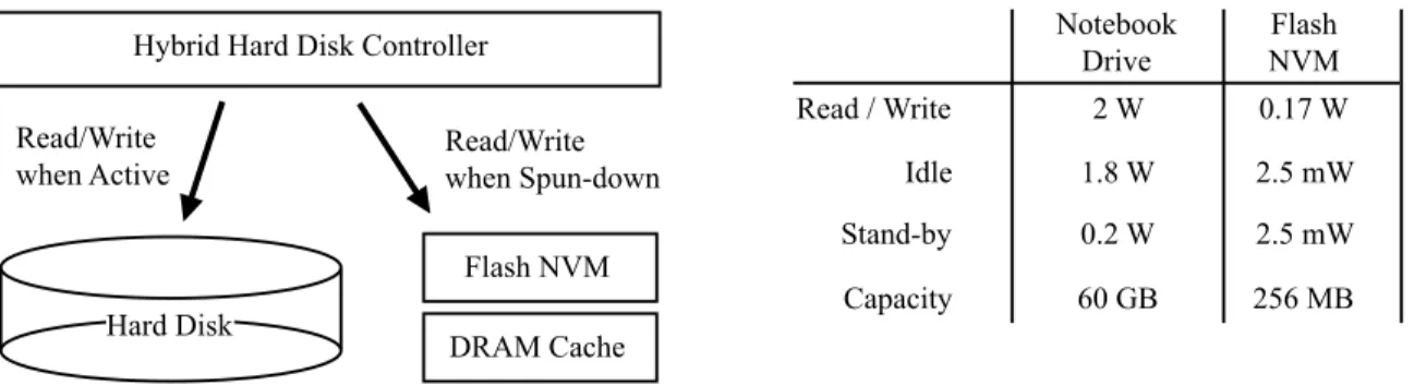
The lack of mechanical components in solid-state disks not only permit better performance, it also results in significantly less power consumption. For example Hitachi Deskstar 7K500 consumes 11-13 W while reading or writing. Its idle average power is 9 W, while it consumes 0.7 W in sleep mode [35]. On the other hand a 64 GB 2.5”
Samsung SSD consumes 1 W (200 mA typical active current operating at 5V) in active mode and 0.1 W in sleep mode [66]. Due to its low power consumption, one of the first proposals to use solid-state disks in storage systems was as a non-volatile cache for hard disks. When flash memory cost was high and density was low, hybrid hard disks were proposed for mobile consumer devices. In these hybrid designs, NAND flash memory was used as a high capacity (higher capacity than DRAM based disk buffers) standby buffer for caching and prefetching data, especially when the hard disk was spun down in
Rotating Disks vs. SSDs
Main take-aways
Forget everything you knew about
rotating disks. SSDs are different
SSDs are complex software systems
One size doesn’t fit all
Rotating Disks vs. SSDs
Main take-aways
Forget everything you knew about
rotating disks. SSDs are different
SSDs are complex software systems
One size doesn’t fit all
Magnet structure of voice coil motor
Spindle & Motor Disk Actuator Flash Memory Arrays Load / Unload Mechanism (a) HDD (b) SSD
sleep mode. This way the hard disk idle times were extended, thus saving power [bisson_2006]. Figure 3.3 shows a typical hybrid disk drive organization and its power specifications.
3.2. Endurance: Reality or Myth?
Hard disk drives has always been prone to endurance or reliability problems due to wear and tear of their mechanical components. Hard disk drive manufacturers have
implemented various techniques to increase the life span of the rotating media and its components. For example head load and unload zones protects disk during idle times, dynamic bearing motors help reduce vibrations and increase operational shock ratings. Today’s hard disk drives typically report three to five years of service life, which is typically defined as the average time period before the probability of mechanical failures substantially increase.
For solid-state disks, reliability and endurance is a different concept. Due to lack of mechanical components solid-state disks are much more reliable and more resistant to shocks compared to hard disk drives. On the other hand, one of the main concerns with
Hard Disk
DRAM Cache Flash NVM Hybrid Hard Disk Controller
Read/Write
when Active Read/Writewhen Spun-down
Read / Write Idle Stand-by Capacity Notebook Drive Flash NVM 2 W 0.17 W 1.8 W 2.5 mW 0.2 W 2.5 mW 60 GB 256 MB
Figure 3.3: Hybrid Hard Disk Organization. An example hybrid hard disk organization with power specifications. Figure adopted from [8]
flash memory is its endurance. A flash memory cell has a lifetime, it can be erased and reprogrammed a limited number of times, after which it can no longer hold a charge. Consumers fear that once they buy a solid-state disk, it will only last a couple of months - a misconception that has slowed down the adoption of NAND flash solid-state disks.
Endurance of flash memory is measured in the number of cycles - the number of write updates on a memory location. Typical NAND flash endurance is 100,000 to 1,000,000 cycles for SLC type and 10,000 to 100,000 for MLC type. For example, assume we have a 64 GB NAND flash memory with an endurance rating of 100,000 cycles. If we are updating the same 64 MB disk block with a sustained write speed of 64 MB per second, then the lifetime of this solid-state disk would only be 28 hours.
Fortunately, flash solid-state disks employ highly optimized wear leveling techniques, which ensure that write updates are written to different physical locations within the disk and each memory cell wears out evenly. When wear leveling techniques are considered, a 64 GB solid-state disk with 100,000 endurance cycles can sustain a 64 MB per second
SSD Capacity Write GB / Day 33 Years 66 Years 112 Years 71 Years 4.8 GB 12.4 GB 20 GB 141 Years 283 Years 183 Years 365 Years 731 Years 256 GB 128 GB 64 GB Professional Student Personal Writes
(GB / Day) 5 YearWrites
12.4 22.6 TB
5.3 9.6 TB
4.4 8 TB
Figure 3.4: SSD Endurance. LDE ratings of a typical SSD based on Bapco mobile user ratings. Figure adopted from [28, 4].
write load for more than 3 years. Moreover if 1,000,000 endurance cycles are taken into account, this will increase to more than 30 years. One metric used by the industry to specify the endurance rating of a solid-state disk is longterm data endurance (LDE). LDE is defined as the total number of writes allowed in SSD’s lifespan [4]. For example, a 32 GB SLC solid-state disk from SanDisk has an LDE spec of 400 TB, and a 64 GB MLC model with 100 TB LDE. If Bapco (Business Applications Performance Corporation) mobile user ratings for a professional is considered, 400 TB LDE corresponds to more than 17 years [4]. A 17 years lifespan for a solid-state disk is much more than a user expected lifespan of a data storage system. With these specifications, one can assume that this limit on the number of writes for NAND flash solid-state disks is theoretical and should not be a concern in the takeover of hard disks. As said by Jim Elliott VP of Marketing from Samsung: “Do you need a million mile auto warranty?” [28].
3.3. SSD Organization
In conventional hard disks, data is stored in disk platters and accessed through read and write heads. Surface number or head number identifies a platter. Each platter has multiple tracks and each track has a number of blocks depending on its zone. Tracks with the same track number in each platter form a cylinder. Access granularity is a sector (block) which has 512 bytes and the location of a block on disk is specified using PBA (Physical Block Address). PBA is formed by a combination of cylinder number, head number, and sector number.
Solid-state disks use a memory array structure different than hard disk drives. NAND flash memory is organized into blocks where each block consists of a fixed
number of pages. Each page stores data and corresponding metadata and ECC
information. A single page is the smallest read and write unit. Data can be read from and written into this memory array via an 8-bit bus. This 8-bit interface is used both for data, address information, and for issuing commands. Flash memory technology does not allow overwriting of data (in-place update of data is not allowed) since a write operation can only change bits from 1 to 0. To change a memory cell’s value from 0 to 1, one has to erase a group of cells first by setting all of them to 1. Also a memory location can be erased a limited number of times, therefore special attention is required to ensure that memory cells are erased uniformly. Despite these differences in storing and accessing data, solid-state disks still assume a block device interface. From host’s file system and virtual memory perspective, there is no difference accessing a HDD or a SSD.
Figure 3.5 shows a 32 GB NAND flash solid-state disk architecture from Samsung [64]. Depending on the capacity of the disk, several flash memory arrays are banged together with dedicated or shared I/O bus. An 8 bit I/O bus is an industry wide
Ctrl IDE ATA SCSI Host x16 SRAM MPU ECC Data Buf fer x32 Flash Translation Layer Data & Ctrl x32 Flash Controller x16 x8 x8 x16 x8 x8 Flash Array Flash Array Flash Array Flash Array Host I/F
Layer NAND I/FLayer
Figure 3.5: Solid-state Disk Organization. Organization of a conventional 32 GB NAND flash SSD. Figure adapted from [64].
several flash memory arrays are organized to achieve desired capacity and bandwidth, they are accessed through NAND interface layer. This layer consists of a flash controller which implements internal read, write and erase commands and controls timing of address, data, and command lines. NAND interface does not specify dedicated lines for address, data, and command signals as an 8 bit I/O bus is shared for all - chip pin count is limited to reduce cost.
NAND flash solid-state disks assume a block device interface. Currently used interfaces are Fiber Channel (FC), parallel SCSI (Small Computer System Interface), parallel ATA (Advanced Technology Attachment), serial ATA (SATA), and serial attached SCSI (SAS). User’s systems (traditionally called host) communicates to the block device through one of these protocols. The host interface layer is responsible for the decoding host system commands and transferring them to a flash translation layer (FTL). FTL layer converts requests’ logical block address into physical page address in the flash memory and initiates read/write commands in the NAND interface layer. Address translation is one of the many activities of FTL later. Although flash memory lacks the mechanical complexities of a conventional hard disk, it has its own peculiarities. Since flash memory does not support the in-place update of data, every write request for a specific logical block address results in data to be written to a different physical address with every update. Therefore, logical to physical address mapping in flash memory is much more complicated and requires a dynamically updated address table. Moreover, FTL also implements wear leveling algorithms. Wear leveling ensures that memory cells in an array are equally used - homogeneous distribution of erase cycles. As mentioned before,
wear leveling is very important in ensuring a long lifespan for solid-state disks. In addition to wear leveling, FTL also implements other features of flash memory such as effective block management, erase unit reclamation, and internal data movements. Also, since there are multiple flash arrays, multiple I/O commands can be processed in parallel for improved performance. FTL layer is responsible in extracting maximum performance by using various types of parallelisms while keeping power consumption and cost at a minimum. One would consider FTL layer as the differentiating factor between different SSD manufacturers as it bundles proprietary firmware.
3.3.1. Flash Memory Array
NAND flash memory is organized into blocks where each block consists of a fixed number of pages. Each page stores data and corresponding metadata and ECC
information. A single page is the smallest read and write unit. Earlier versions of flash memory had page sizes of 512 Bytes and block sizes of 16 KBytes (32 pages). Currently a typical page size is 2 KBytes (4 sectors of 512 Bytes each), and a typical block size is 128 KBytes (64 pages). The number of blocks and pages vary with the size of the flash memory chip. Earlier flash devices with 512 Bytes page sizes are usually referred to as small-block NAND flash devices and devices with 2 KBytes page sizes are referred to as large-block. In addition to storage cells for data and metadata information, each memory die includes a command register, an address register, a data register, and a cache register. Figure 3.6 shows NAND flash memory array organization for a sample 1 Gbit flash memory from Micron [59]. Larger density flash arrays are usually manufactured by combining several lower density flash arrays in a single die - multiple planes in a die. For
example, 2 Gbit Micron flash memory is two 1 Gbit arrays on a single die (2 planes in a die). Furthermore, two dies can be stacked together to form a 4 Gbit flash memory. These two dies can operate independently or together, depending on the model and
configuration. Figure 3.6 also shows 16 Gbit flash devices from Samsung and Toshiba, where multiple planes are visible. Samsung’s 16 Gbit NAND flash is MCL type and
33 I/O Control I/O Column Row Data Reg Cache Reg Control Logic Cmd Reg Status Reg Addr Reg CE# W# R#
Flash Memory Bank
Data Reg Cache Reg 2K bytes 1 Block 1 Page = 2 K bytes 1 Blk = 64 Pages
1024 Blocks per Device (1 Gb)
Flash Array
Fig. 7. A 2-GbitNANDFlash memory using 90 nm technology. Volume production is in 2003.
Fig. 8. NANDFlash memory technology roadmap.
Fig. 9. High-density memory production roadmap.
Flash memory technology, ArF will be used for lithography, while KrF is for the 90-nm technology. The pure tungsten is being considered to reduce the resistance of the word line. For the cutting-edge multilevel cell (MLC), the threshold voltage (Vth) uniformity must be ensured.
Fig. 10. High-density memory growth will surpass the prediction from Moore’s law.
III. NEWMEMORYGROWTHMODEL IN THEERA OF
NANOTECHNOLOGY
Based on the discussions in Section II, the overall memory production roadmap is shown in Fig. 9. Even though the (a) 1 Gbit Flash Memory
(b) 2 Gbit Flash Memory
1/18/09 10:00 AM EETimes.com - 16-Gbit MLC NAND flash weighs in
Page 1 of 4 http://www.eetimes.com/showArticle.jhtml?articleID=201200825
For a full archive of articles and related On-Demand seminars, click here
Your ad here. Buy Media Now
EE Times:
16-Gbit MLC NAND flash weighs in
Young Choi, Semiconductor Insights
EE Times
(07/30/2007 9:00 AM EDT)
To meet increasing demand for more digital storage, leading flash memory manufacturers are touting their latest single-chip 16-Gbit MLC NAND flash devices. Earlier this year, Toshiba announced a 16-Gbit MLC NAND flash manufactured in the 56-nm process node. Samsung, meanwhile, introduced a 16-Gbit MLC NAND flash using a 51-nm process, a half a process node ahead of Toshiba's.
Developing MLC NAND flash memories within the 50-nm range process node requires overcoming many technical challenges, from both a process and
circuit design perspective. Some of the issues that must be addressed are the
proper layout design of bitlines and surrounding dummy patterns; the placement of P-well bias; efficient self-boosting circuitry for row decoder and wordline switches; efficient and reliable high-voltage pump circuitry; and efficient read, programming, erase and verify algorithms to guarantee reliable operations with reduced charges stored in smaller flash memory cells.
Semiconductor Insights has analyzed the latest 16-Gbit MLC NAND flash devices from both Toshiba and Samsung. Initial results showed that both devices achieved impressive die area and Mbit/mm ratings for storage with some architectural changes from previous designs. More details of the new designs will be disclosed after further analyses of the architecture and circuits, process and device characteristics, and waveform analysis to show the innovations Samsung and Toshiba have made.
Samsung 16-Gbit NAND
In its latest 16-Gbit MLC NAND flash device, Samsung has simplified the floor plan and architecture from the previous-generation 65-nm 8-Gbit MLC NAND flash device. There are two row decoder areas, which split the memory array into four 4-Gbit arrays. Page buffers are now all consolidated in one side of the chip, as opposed to having two halves on either side of the memory array in the previous-generation product.
Die photograph of Samsung's 51-nm 16-Gbit MLC NAND flash device.
Samsung still has the bonding pads on both sides of the chip, but the 16-Gbit device has pads on both edges in the wordline direction, apparently to improve power distribution. The previous generation has pads in the bitline direction.
Your ad here. Buy Media Now
INDUSTRY SUPPLIERS
Solid State Drives for high performance, endurance & reliability of laptop applications - Toshiba NAND
Get a better disk drive alternative with embedded high-capacity, on-board memory - Toshiba NAND
Meet your electronic design challenges with our range of solution providers - Industry Suppliers
More Industry Suppliers »
Related Products • 1.5A step down regulator supports green home/office appliances • 3-mm infrared emitter delivers 65-mW/sr radiant intensity • Optimized AV codecs for streamlined multimedia product development • Image sensor boasts better sensitivity for webcams, surveillance, automotive and toys
• Phyworks shifts transceivers design to CMOS
Marketplace
Download ADI’s VisualDSP++ Development Software
Use VisualDSP++ software for ADI processors in a wide range
FEATURED TOPIC
ADDITIONAL TOPICS Embedded Forum: Solve your design challenges today Get expert advice on your embedded design at the
Ready for a change? Open | Close
CAREER CENTER
1/18/09 10:00 AM EETimes.com - 16-Gbit MLC NAND flash weighs in
Page 2 of 4 http://www.eetimes.com/showArticle.jhtml?articleID=201200825
direction.
Toshiba 16-Gbit NAND
Toshiba's latest device has the same overall architecture and floor plan as its previous-generation 70-nm 8-Gbit MLC NAND flash. The page buffer size has been increased to 4 kbytes from 2 kbytes. The chip has two 8-Gbit flash memory arrays divided by row decoders.
Die photograph of Toshiba's 56-nm 16-Gbit MLC NAND flash device. As with the preceding device, all bonding pads are in one side of the chip. Toshiba appears to have a different architecture in its 8-Gbit manufactured in the same 56-nm process node. According to an "IEEE Journal of Solid-State Circuits" paper published in January, the 8-Gbit design appeared to have 4 kbytes of page buffers located between two 4-Gbit flash memory arrays. In 16-Gbit design, however, the page buffers are along the side where the bonding pads are, and the row decoders are between two 8-Gbit arrays. By placing row decoders, page buffers and all bonding pads on one side, the latest Toshiba 16-Gbit device achieved efficient floor plan with only 173mm2
of chip size. Toshiba apparently has overcome challenges with internal power distribution and stability by putting all power pads on one side of the chip. By migrating their production to 5x-nm process node, both Samsung and Toshiba have achieved 40 percent improvement of Mbit/mm2 with only a 20
percent increase in chip size from their previous 8-Gbit designs. Samsung's design appears to have achieved about a 5 percent smaller chip size due to its smaller feature-size advantage over Toshiba.
(Click on image to enlarge)
Road map to more bits per cell
While flash makers continue to develop more advanced flash technology beyond 40 nm and 30 nm, increasing bit density by enhancing MLC technology to 3 bits per cell is being pursued at the 5x-nm process node. Toshiba and SanDisk are reportedly developing 3-bit-per-cell technology at their 56-nm process node to develop a 24-Gbit flash memory device. The 3-bit MLC technology will also produce 48-G3-bit MLC NAND flash memories in the 40-nm generation.
Precise placement of eight unique threshold voltages to the flash memory cells and performing error correction would be challenges for developing 3-bit technology. The 4-bit technology is expected to emerge at the 40-nm process node. MLC technology for 3 bits per cell and 4 bits per cell is expected to be critical for companies to remain competitive in 2009 through 2011.
Other challenges
Availability of single-chip 16-Gbit MLC NAND flash memory devices is expected to stimulate the market for applications such as solid-state disk and hybrid hard drive. Samsung has announced a 64-Gbyte SSD using the latest 51-nm 8-Gbit SLC flash devices (equivalent to 16-Gbit MLC). Intel, for its part, has its Turbo Memory support for Windows Vista. SSD's faster boot times and application startup times, and its enhanced reliability and battery life, should spur the adoption of SSDs and HHDs in the notebook market.
ADI processors in a wide range of applications. Register Today! Advertise With Us
Variability Aware Modeling and Characterization in Standard Cell in 45 nm CMOS with Stress Enhancement Technique The basics of phase change memory (PCM) technology 10 Tips for Creating an Exceptional Electronics White Paper
All White Papers »
Embedded Forum Get advice on COM Express design at the Embedded Forum Whitepaper on industrial multicore performance Discussion: new generation of solution for mid-size VPN appliances Sponsored Products Site Features Calendar Events Conference Coverage Forums Career Center Multimedia Column Archive Special Reports Subscriptions Print | Digital RSS Samsung 16 Gbit (4x4 Gbit) Toshiba 16 Gbit (2x8 Gbit)
(c) 16 Gbit Flash Memory
Figure 3.6: Flash Memory Array. (a) NAND flash memory organization. A typical 1 Gb flash memory array consists of 1024 blocks. Each block contains 64 pages of 2 KB each. Figure adapted from [59]. (b) Sample 2 Gbit NAND flash memory in production in 2003 using 90 nm technology [39]. (c) Die photograph of Samsung’s 51 nm and Toshiba’s 56 nm 16 Gbit NAND flash memory chips [20].
manufactured using 51 nm technology. 16 Gbit is divided into 4 4-Gbit arrays. Page buffers are all in one side of the device but bonding pads are located in both sides for better power distribution. Toshiba’s 16 Gbit NAND flash is also MLC type but
manufactured using 56 nm technology. It uses two 8-Gbit memory arrays. One difference with this device is that data and cache registers are 4 KB instead of the more common 2 KBytes [20]. This suggests that each of two 8-Gbit arrays is indeed a two plane memory array operating in synch - 2 KBytes data and cache registers from both planes are combined and operate as one.
3.3.2. NAND Flash Interface
NAND flash memory supports 3 operations: read, write (program), and erase. 8 bit I/O bus is used for the interface without any dedicated address and command lines. As mentioned before, the smallest access unit for read and write is a page and erase operation is applied to an entire block.
To read a page, one issues a read command to the command register and writes the block number and the page number within the block into the address register. Complete page data (2 KBytes) will be accessed in tR time and will be loaded into the
data register. The typical value for tR is 25 µs. Afterwards data can be read from data
register via 8 bit I/O bus by repeatedly pulsing RE (Read Enable) signal at the maximum tRC rate. Earlier solid-state disks could pulse RE at a rate of 20 MHz. Currently, a 33 or
50 MHz rate is common. In addition to a read command, NAND flash interface also supports random read and read cache mode operations. Random read can be used when only a sector is required from a page. When a page is accessed and loaded into the data
register, a specific sector (512 Bytes) within the page can be addressed and transferred via I/O bus. If sequential pages need to be accessed, the read command can be used in cache mode to increase the data transfer rate. In this mode, when the first page is loaded into the data register, it will be transferred from the data register to the cache register. Typically, copying data from the data register to the cache register takes 3 µs. While data is being read out from the cache register by pulsing RE, subsequent page can be accessed and loaded into the data register. Depending on the manufacturer, read in cache mo


![Figure 2.5: NAND and NOR flash density comparison. 64 MB NAND chip is about a third of the size of a 64 MB NOr chip [msystems2003comparison].](https://thumb-us.123doks.com/thumbv2/123dok_us/716083.2589373/24.918.172.645.107.451/figure-nand-flash-density-comparison-nand-msystems-comparison.webp)
![Figure 2.6: NAND flash scaling. Historical trend of NAND flash memory technology and cell size reduction [39, 74]](https://thumb-us.123doks.com/thumbv2/123dok_us/716083.2589373/27.918.166.807.120.353/figure-nand-flash-scaling-historical-memory-technology-reduction.webp)


![Figure 2.8: SLC and MLC NAND flash chips. Figure adopted from [78].](https://thumb-us.123doks.com/thumbv2/123dok_us/716083.2589373/30.918.167.784.107.380/figure-slc-mlc-nand-flash-chips-figure-adopted.webp)