B
R O A D C A S T
M
E C H A N I C A L
T
U N I N G
A M / F M / S W R
A D I O
R
E C E I V E R
Features
Applications
Description
The Si4831/35-B30 is the 2nd generation mechanical-tuned digital CMOS AM/FM/SW radio receiver IC that integrates the complete receiver function from antenna input to audio output. Like other successful audio products from Silicon Labs, Si4831/35-B30 offers unmatched integration and PCB space savings with minimum external components and a small board area. The Si4831/35-B30 requires a simple application circuit and removes any requirements for manually tuning components during the manufacturing process. The Si4831/35-B30 is a very simple product to design, manufacture, and support across multiple product lines. The receiver has very low power consumption, runs off two AAA batteries, and delivers the performance benefits of digital tuning to the analog radio market.
Functional Block Diagram
Worldwide FM band support(64–109 MHz)
Worldwide AM band support (504–1750 kHz)
SW band support (Si4835 only) (5.6–22 MHz)
Excellent real-world performance EN55020-compliant
No manual alignment necessary Flexible band selections
Automatic frequency control (AFC) Integrated LDO regulator
2.0 to 3.6 V supply voltage
Wide range of ferrite loop sticks and air loop antennas supported
24-pin SSOP RoHS-compliant
Supports station and stereo LED indicators
Direct volume control Bass and treble tone control
Table and portable radios Stereos Mini/micro systems CD/DVD players Boom boxes Modules Clock radios Mini HiFi Entertainment systems Si4830/34 ADC ADC DSP DAC DAC ROUT LOUT AFC Si4831/35 RFGND LNA AMI AGC REG VDD1/2 2.0~3.6V XTAL OSC FMI 0/90 ADC XTALI AM ANT FM/SW ANT CONTROL INTERFACE TUNE 1/2 BAND
This product, its features, and/or its architecture is covered by one or more of the following patents, as well as other patents, pending and issued, both foreign and domestic: 7,127,217; 7,272,373; 7,272,375; 7,321,324; 7,355,476; 7,426,376; 7,471,940; 7,339,503; 7,339,504. Ordering Information: See page 13. Pin Assignments Si4831/35-B30 (SSOP) NC FMI RFGND AMI BAND TUNE2 TUNE1 STATION STEREO NC NC NC RST LOUT ROUT DBYP VDD2 VOL+/TREBLE VOL-/BASS XTALO XTALI VDD1 GND GND 1 2 3 4 5 6 7 8 9 10 11 12 24 23 22 21 20 19 18 17 16 15 14 13
T
A B L E
O F
C
O N T E N TS
Section
Page
1. Electrical Specifications . . . 4
2. Typical Application Schematic . . . 8
3. Bill of Materials . . . 9
4. Functional Description . . . 10
4.1. Overview . . . .10
4.2. FM Receiver . . . .10
4.3. AM Receiver . . . .11
4.4. SW Receiver . . . .11
4.5. Frequency Tuning . . . .11
4.6. Band Select . . . .11
4.7. Bass and Treble . . . .11
4.8. Volume Control . . . .11
5. Pin Descriptions: Si4831/35-B30 . . . 12
6. Ordering Guide . . . 13
7. Package Markings (Top Marks) . . . 14
7.1. Si4831/35-B30 Top Mark . . . .14
7.2. Top Mark Explanation . . . .14
8. Package Outline: Si4831/35-B30 . . . 15
9. PCB Land Pattern: Si4831/35-B30 . . . 16
10. Additional Reference Resources . . . 17
Document Change List . . . 18
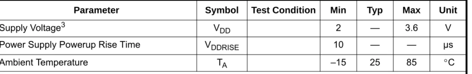
1. Electrical Specifications
Table 1. Recommended Operating Conditions
1,2Parameter Symbol Test Condition Min Typ Max Unit
Supply Voltage3 VDD 2 — 3.6 V
Power Supply Powerup Rise Time VDDRISE 10 — — µs
Ambient Temperature TA –15 25 85 C
Note:
1. Typical values in the data sheet apply at VDD = 3.3 V and 25 °C unless otherwise stated.
2. All minimum and maximum specifications in the data sheet apply across the recommended operating conditions for minimum VDD= 2.7 V.
3. Operation at minimum VDD is guaranteed by characterization when VDD voltage is ramped down to 2.0 V. Part initialization may become unresponsive below 2.3 V.
Table 2. Absolute Maximum Ratings
1,2Parameter Symbol Value Unit
Supply Voltage VDD –0.5 to 5.8 V Input Current3 IIN 10 mA Operating Temperature TOP –40 to 95 C Storage Temperature TSTG –55 to 150 C RF Input Level4 0.4 VPK Notes:
1. Permanent device damage may occur if the above Absolute Maximum Ratings are exceeded. Functional operation should be restricted to the conditions as specified in the operational sections of this data sheet. Exposure beyond recommended operating conditions for extended periods may affect device reliability.
2. The Si4831/35-B30 devices are high-performance RF integrated circuits with certain pins having an ESD rating of < 2 kV HBM. Handling and assembly of these devices should only be done at ESD-protected workstations.
3. For input pins RST, VOL+/TREBLE, VOL–/BASS, XTALO, XTALI, BAND, TUNE2, TUNE1, STATION, and STEREO. 4. At RF input pins, FMI and AMI.
Figure 1. Reset Timing
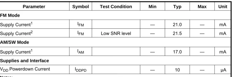
Table 3. DC Characteristics
(VDD= 2.7 to 3.6 V, TA= –15 to 85 °C)
Parameter Symbol Test Condition Min Typ Max Unit
FM Mode
Supply Current1 IFM — 21.0 — mA
Supply Current2 IFM Low SNR level — 21.5 — mA
AM/SW Mode
Supply Current1 IAM — 17.0 — mA
Supplies and Interface
VDD Powerdown Current IDDPD — 10 — µA
Notes:
1. Specifications are guaranteed by characterization.
2. LNA is automatically switched to higher current mode for optimum sensitivity in weak signal conditions.
Table 4. Reset Timing Characteristics
(VDD = 2.7 to 3.6 V, TA = –15 to 85 °C)
Parameter Symbol Min Typ Max Unit
RST Pulse Width and TUNE1, TUNE2 Setup to RST tSRST 100 — — µs
TUNE1, TUNE2 Hold from RST tHRST 30 — — ns
70% 30%
TUNE1
70% 30%TUNE2
70% 30% tSRSTRST
tHRSTTable 5. FM Receiver Characteristics
1,2(VDD = 2.7 to 3.6 V, TA = –15 to 85 °C)
Parameter Symbol Test Condition Min Typ Max Unit
Input Frequency fRF 64 — 109 MHz
Sensitivity with Headphone Network3
(S+N)/N = 26 dB — 2.2 — µV EMF
LNA Input Resistance4,5 — 4 — k
LNA Input Capacitance4,5 — 5 — pF
AM Suppression4,5,6,7 m = 0.3 — 50 — dB
Input IP34,8 — 105 — dBµV EMF
Adjacent Channel Selectivity4 ±200 kHz — 50 — dB
Alternate Channel Selectivity4 ±400 kHz — 65 — dB
Audio Output Voltage5,6,7 — 80 — mVRMS
Audio Mono S/N5,6,7,9,10 — 55 — dB
Audio Stereo S/N3,4,5,7,9,10, — 55 — dB
Audio Frequency Response Low –3 dB — — 30 Hz
Audio Frequency Response High –3 dB 15 — — kHz
Audio Stereo Separation5,11 — 42 — dB
Audio THD6,5,11 — 0.1 0.5 %
Audio Output Load Resistance4,10 RL Single-ended 10 — — k
Audio Output Load Capacitance4,10 CL Single-ended — — 50 pF
Powerup/Band Switch Time4 — — 110 ms
Notes:
1. Additional testing information is available in “AN569: Si4831/35-DEMO Board Test Procedure.”Volume = maximum for all tests. Tested at RF = 98.1 MHz.
2. To ensure proper operation and receiver performance, follow the guidelines in “AN555: Si483x-B Antenna, Schematic, Layout, and Design Guidelines.” Silicon Laboratories will evaluate schematics and layouts for qualified customers. 3. Frequency is 76~109 MHz.
4. Guaranteed by characterization. 5. VEMF= 1 mV.
6. FMOD= 1 kHz, MONO, and L = R unless noted otherwise. 7. f = 22.5 kHz.
8. |f2 – f1| > 2 MHz, f0= 2 x f1 – f2. 9. BAF= 300 Hz to 15 kHz, A-weighted. 10. At LOUT and ROUT pins.
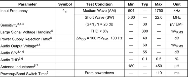
Table 6. AM/SW Receiver Characteristics
1, 2(VDD = 2.7 to 3.6 V, TA = –15 to 85 °C)
Parameter Symbol Test Condition Min Typ Max Unit
Input Frequency fRF Medium Wave (AM) 504 — 1750 kHz
Short Wave (SW) 5.60 — 22.0 MHz
Sensitivity3,4,5 (S+N)/N = 26 dB — 30 — µV EMF
Large Signal Voltage Handling5 THD < 8% — 300 — mVRMS
Power Supply Rejection Ratio5 ∆VDD= 100 mVRMS, 100 Hz — 40 — dB
Audio Output Voltage3,6 — 60 — mVRMS
Audio S/N3,4,6 — 55 — dB
Audio THD3,6 — 0.1 0.5 %
Antenna Inductance5,7 180 — 450 µH
Powerup/Band Switch Time5 From powerdown — — 110 ms
Notes:
1. Additional testing information is available in “AN569: Si4831/35-DEMO Board Test Procedure.” Volume = maximum for all tests. Tested at RF = 520 kHz.
2. To ensure proper operation and receiver performance, follow the guidelines in “AN555: Si483x-B Antenna, Schematic, Layout, and Design Guidelines.” Silicon Laboratories will evaluate schematics and layouts for qualified customers. 3. FMOD = 1 kHz, 30% modulation, 2 kHz channel filter.
4. BAF= 300 Hz to 15 kHz, A-weighted. 5. Guaranteed by characterization. 6. VIN= 5 mVrms.
7. Stray capacitance on antenna and board must be < 10 pF to achieve full tuning range at higher inductance levels.
Table 7. Reference Clock and Crystal Characteristics
(VDD = 2.7 to 3.6 V, TA = –15 to 85 °C)
Parameter Symbol Test Condition Min Typ Max Unit
Reference Clock XTALI Supported Reference Clock
Frequencies — 32.768 — kHz
Reference Clock Frequency Tolerance for XTALI
–100 — 100 ppm
Crystal Oscillator
Crystal Oscillator Frequency — 32.768 — kHz
Crystal Frequency Tolerance –100 — 100 ppm
2. Typical Application Schematic
Notes:
1. Place C4 close to VDD2 and DBYP pins.
2. All grounds connect directly to GND plane on PCB. 3. Pin 6 and 7 leave floating.
4. To ensure proper operation and receiver performance, follow the guidelines in "AN555: Si483x-B Antenna, Schematic, Layout, and Design Guidelines." Silicon Labs will evaluate the schematics and layouts for qualified customers.
5. Pin 8 connects to the FM antenna interface and pin 12 connects to the AM antenna interface.
6. Place Si483x as close as possible to antenna jack and keep the FMI and AMI traces as short as possible.
5
RFGND
Optional: AM air loop antenna
2.0 TO 3.6V 2.0 TO 3.6V Optional (Si4835 only) 2. 5k /100M FM AM BAND Y1 32.768KHz C2 22p C3 22p 1 ST EREO 2 ST AT IO N 3 TU NE 1 4 TU NE 2 5 BA ND 6 NC 7 NC 8 FM I 9 RF GND 10 NC 11 NC 12 AM I 13 GND 14 GND 15 RS T 16 VO L+/T REB LE 17 VOL -/ BA SS 18 XT AL 0 19 XT AL I 20 VDD1 21 VDD2 22 DB YP 23 RO UT 24 LO UT U1 C5 0.47u AN T1 AM a nt enna ANT2 T1 C 0.47u C4 0.1u C1 0.1u R1 100k VR1 100k B1 1 2 3 S2 R3 253k R4 180k R5 67k R2 10k VD D VD D STATION_LED STEREO_LED FMI LOUT ROUT AMI AMI VDD VDD BA ND TU NE 1 TUNE1
3. Bill of Materials
Table 8. Si4831/35-B30 Bill of Materials
Component(s) Value/Description Supplier
C1 Reset capacitor 0.1 uF, ±20%, Z5U/X7R Murata
C4 Supply bypass capacitor, 0.1 uF, ±20%, Z5U/X7R Murata
C5 Coupling capacitor, 0.47 µF, ±20%, Z5U/X7R Murata
B1 Ferrite bead 2.5k/100 MHz Murata
VR1 Variable resistor (POT), 100k, ±10% Kennon
R1 Reset timing resistor, 100k, ±5% Venkel
R2 Resistor, 10k, ±5% Venkel
R3 Resistor, 253k, ±1% Venkel
R4 Resistor, 180k, ±1% Venkel
R5 Resistor, 67k, ±1% Venkel
U1 Si4831/35-B30 Mechanical Tuning Radio Receiver Silicon Laboratories
S2 Band switch Any, depends on
customer
ANT1 Ferrite stick,180-450 µH Jiaxin
Optional Components
C2, C3 Crystal load capacitors, 22 pF, ±5%, COG
(Optional: for crystal oscillator option)
Venkel
Y1 32.768 kHz crystal (Optional: for crystal oscillator option) Epson or equivalent
4. Functional Description
Figure 2. Si4831/35-B30 Functional Block Diagram
4.1. Overview
The Si4831/35-B30 is the industry's most advanced fully integrated, mechanical-tuned 100% CMOS AM/FM/SW radio receiver IC. Offering unmatched integration and PCB space savings, the Si4831/35-B30 requires minimum external components and a small board area. The Si4831/35-B30 AM/FM/SW radio provides space savings and low power consumption while delivering the high performance and design simplicity desired for all AM/FM/SW solutions.
Leveraging Silicon Laboratories' proven and patented digital low intermediate frequency (low-IF) receiver architecture, the Si4831/35-B30 delivers superior RF performance and interference rejection in AM, FM, and SW bands. The high integration and complete system production test simplifies design-in, increases system quality, and improves manufacturability.
4.2. FM Receiver
The Si4831/35-B30 integrates a low noise amplifier (LNA) supporting the worldwide FM broadcast band (64 to 109 MHz).
Pre-emphasis and de-emphasis is a technique used by FM broadcasters to improve the signal-to-noise ratio of FM receivers by reducing the effects of high frequency interference and noise. When the FM signal is transmitted, a pre-emphasis filter is applied to accentuate the high audio frequencies. All FM receivers incorporate a de-emphasis filter which attenuates high frequencies to restore a flat frequency response. Two time constants are used in various regions. The de-emphasis time constant can be chosen to be 50 or 75 µs. Refer to "AN555: Si483x-B Antenna, Schematic, Layout, and Design Guidelines."
The Si4831/35-B30 also has advanced stereo blending that employs adaptive noise suppression. As a signal quality degrades, the Si4831/35-B30 gradually combines the stereo left and right audio channels to a mono audio signal to maintain optimum sound fidelity under varying reception conditions. The Si4831/35-B30 can drive a stereo light with the stereo/mono information so that the user can easily discern the signal quality.
Si4830/34
ADC ADC DSP DAC DAC ROUT LOUT AFCSi4831/35
RFGND LNA AMI AGC REG VDD1/2 2.0~3.6V XTAL OSC FMI 0/90 ADC RST XTALI AM ANT FM/SW ANT CONTROL INTERFACE ST ATIO N STEREO VO L/ TO NE TUNE 1/2 BANDThe stereo light up criteria is defined using both RSSI and the Left and Right separation levels as these two specifications are the primary factors for stereo listening. The criteria can be set between two conditions: the Left and Right channels are separated by more than 6 dB with RSSI at >20 dB or Left and Right channels are separated by more than 12 dB with RSSI at >28 dB. The selection can be set up using different values of the external resister. Refer to "AN555: Si483x-B Antenna, Schematic, Layout, and Design Guidelines."
4.3. AM Receiver
The highly integrated Si4831/35-B30 supports worldwide AM band reception from 504 to 1750 kHz with five sub-bands using a digital low-IF architecture with a minimum number of external components and no manual alignment required. This patented architecture allows for high-precision filtering, offering excellent selectivity and SNR with minimum variation across the AM band. Similar to the FM receiver, the Si4831/35-B30 optimizes sensitivity and rejection of strong interferers, allowing better reception of weak stations.
To offer maximum flexibility, the receiver supports a wide range of ferrite loop sticks from 180–450 µH. An air loop antenna is supported by using a transformer to increase the effective inductance from the air loop. Using a 1:5 turn ratio inductor, the inductance is increased by 25 times and easily supports all typical AM air loop antennas, which generally vary between 10 and 20 µH.
4.4. SW Receiver
The Si4835 supports 16 short wave (SW) band receptions from 5.60 to 22.0 MHz. Si4835 supports extensive short wave features such as minimal discrete components and no factory adjustments. The Si4835 supports using the FM antenna to capture short wave signals.
4.5. Frequency Tuning
A valid channel can be found by tuning the potentiometer that is connected to the TUNE1 and TUNE2 pin of the Si4831/35-B30 chip.
To offer easy tuning, the Si4831/35-B30 also supports a station LED light. It will light up the LED if the RF signal quality passes the LED sensitivity threshold when tuned to a valid station.
4.6. Band Select
The Si4831/35-B30 supports worldwide AM band with five sub-bands, US/Europe/Japan/China FM band with five sub-bands, and SW band with 16 sub-bands. For details on band selection, refer to "AN555: Si483x-B Antenna, Schematic, Layout, and Design Guidelines."
4.7. Bass and Treble
The Si4831/35-B30 further supports bass and treble tone control for superior sound quality. Pins 16 and 17 can be configured for tone control, allowing customers to use either two buttons or one slide-switch to adjust the bass and treble. For further configuration details, refer to "AN555: Si483x-B Antenna, Schematic, Layout, and Design Guidelines."
4.8. Volume Control
The Si4831/35-B30 not only allows customers to use the traditional PVR wheel volume control through an external speaker amplifier, it also supports direct digital volume control through pins 16 and pin 17 by using volume up and down buttons. Refer to "AN555: Si483x-B Antenna, Schematic, Layout, and Design Guidelines."
5. Pin Descriptions: Si4831/35-B30
Pin Number(s) Name Description
1 STEREO Stereo indicator
2 STATION Station indicator
3 TUNE1 Frequency tuning
4 TUNE2 Frequency tuning
5 BAND Band selection and De-emphasis/Stereo separation selection
6,7 NC No connect. Leave floating.
8 FMI FM RF inputs. FMI should be connected to the antenna trace.
9 RFGND RF ground. Connect to ground plane on PCB.
10,11 NC Unused. Tie these pins to GND.
12 AMI AM RF input. AMI should be connected to the AM antenna.
13,14 GND Ground. Connect to ground plane on PCB.
15 RST Device reset (active low) input
16 VOL+/TREBLE Volume button up/Treble
17 VOL–/BASS Volume button down/Bass
18 XTALO Crystal oscillator output
19 XTALI Crystal oscillator input
20 VDD1 Supply voltage. May be connected directly to battery.
21 VDD2 Supply voltage. May be connected directly to battery.
22 DBYP Dedicated bypass for VDD
23 ROUT Right audio line output in analog output mode
24 LOUT Left audio line output in analog output mode
NC
FMI
RFGND
AMI
BAND
TUNE2
TUNE1
STATION
STEREO
NC
NC
NC
RST
LOUT
ROUT
DBYP
VDD2
VOL+/TREBLE
XTALO
XTALI
VDD1
GND
GND
1 2 3 4 5 6 7 8 9 10 11 12 24 23 22 21 20 19 18 17 16 15 14 13VOL-/BASS
6. Ordering Guide
Part Number* Description Package
Type
Operating Temperature/Voltage
Si4831-B30-GU AM/FM Broadcast Radio Receiver 24L SSOP
Pb-free
–15 to 85 °C 2.0 to 3.6 V
Si4835-B30-GU AM/FM/SW Broadcast Radio Receiver 24L SSOP
Pb-free
–15 to 85 °C 2.0 to 3.6 V
*Note: Add an “(R)” at the end of the device part number to denote tape and reel option. The devices will typically operate at 25 °C with degraded specifications for VDD voltage ramped down to 2.0 V.
7. Package Markings (Top Marks)
7.1. Si4831/35-B30 Top Mark
7.2. Top Mark Explanation
Mark Method: YAG Laser
Line 1 Marking: Device identifier 4831B30GU = Si4831-B30
4835B30GU = Si4835-B30 Line 2 Marking:
YY = Year
WW = Work week
TTTTTT = Manufacturing code
Assigned by the Assembly House.
4831B30GU
YYWWTTTTTT
4835B30GU
YYWWTTTTTT
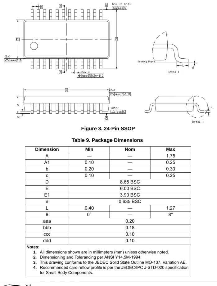
8. Package Outline: Si4831/35-B30
The 24-pin SSOP illustrates the package details for the Si4831/35-B30. Table 9 lists the values for the dimensions shown in the illustration.
Figure 3. 24-Pin SSOP
Table 9. Package Dimensions
Dimension Min Nom Max
A — — 1.75 A1 0.10 — 0.25 b 0.20 — 0.30 c 0.10 — 0.25 D 8.65 BSC E 6.00 BSC E1 3.90 BSC e 0.635 BSC L 0.40 — 1.27 θ 0° — 8° aaa 0.20 bbb 0.18 ccc 0.10 ddd 0.10 Notes:
1. All dimensions shown are in millimeters (mm) unless otherwise noted. 2. Dimensioning and Tolerancing per ANSI Y14.5M-1994.
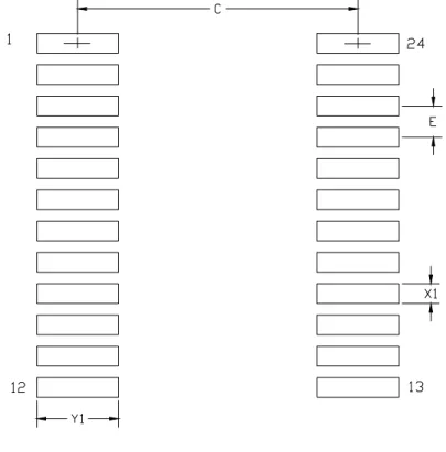
9. PCB Land Pattern: Si4831/35-B30
Figure 4, “PCB Land Pattern,” illustrates the PCB land pattern details for the Si4831/35-B30-GU SSOP. Table 10 lists the values for the dimensions shown in the illustration.
Figure 4. PCB Land Pattern
Table 10. PCB Land Pattern Dimensions
Dimension Min Max
C 5.20 5.40
E 0.65 BSC
X1 0.35 0.45
Y1 1.55 1.75
General:
1. All dimensions shown are in millimeters (mm) unless otherwise noted. 2. This land pattern design is based on the IPC-7351 guidelines. Solder Mask Design:
3. All metal pads are to be non-solder mask defined (NSMD). Clearance between the solder mask and the metal pad is to be 60 µm minimum, all the way around the pad. Stencil Design:
4. A stainless steel, laser-cut, and electro-polished stencil with trapezoidal walls should be used to assure good solder paste release.
5. The stencil thickness should be 0.125 mm (5 mils).
6. The ratio of stencil aperture to land pad size should be 1:1 for all perimeter pads. Card Assembly:
7. A No-Clean, Type-3 solder paste is recommended.
8. The recommended card reflow profile is per the JEDEC/IPC J-STD-020 specification for Small Body Components.
10. Additional Reference Resources
Contact your local sales representatives for more information or to obtain copies of the following references:
EN55020 Compliance Test Certificate
AN555: Si483x-B Antenna, Schematic, Layout, and Design Guidelines
AN569: Si4831/35-DEMO Board Test Procedure
D
OCUMENT
C
HANGE
L
IST
Revision 0.1 to Revision 0.7
Updated block diagram.
Updated application schematic. Updated bill of materials.
Updated Section “4.2. FM Receiver”.
Updated Section “4.3. AM Receiver”.
Updated Section “4.6. Band Select”.
Revision 0.7 to Revision 1.0
Updated block diagram
Updated Table 2, “Absolute Maximum Ratings1,2,”
on page 4
Updated Table 5, “FM Receiver Characteristics1,2,”
on page 6
Updated Table 6, “AM/SW Receiver Characteristics1,
2,” on page 7
Updated “4. Functional Description”
C
ONTACT
I
NFORMATION
Silicon Laboratories Inc. 400 West Cesar Chavez Austin, TX 78701 Tel: 1+(512) 416-8500 Fax: 1+(512) 416-9669 Toll Free: 1+(877) 444-3032 Email: [email protected] Internet: www.silabs.com
Silicon Laboratories and Silicon Labs are trademarks of Silicon Laboratories Inc.
Other products or brandnames mentioned herein are trademarks or registered trademarks of their respective holders.
The information in this document is believed to be accurate in all respects at the time of publication but is subject to change without notice. Silicon Laboratories assumes no responsibility for errors and omissions, and disclaims responsibility for any consequences resulting from the use of information included herein. Additionally, Silicon Laboratories assumes no responsibility for the functioning of undescribed features or parameters. Silicon Laboratories reserves the right to make changes without further notice. Silicon Laboratories makes no warranty, rep-resentation or guarantee regarding the suitability of its products for any particular purpose, nor does Silicon Laboratories assume any liability arising out of the application or use of any product or circuit, and specifically disclaims any and all liability, including without limitation conse-quential or incidental damages. Silicon Laboratories products are not designed, intended, or authorized for use in applications intended to support or sustain life, or for any other application in which the failure of the Silicon Laboratories product could create a situation where per-sonal injury or death may occur. Should Buyer purchase or use Silicon Laboratories products for any such unintended or unauthorized ap-plication, Buyer shall indemnify and hold Silicon Laboratories harmless against all claims and damages.