10/11/2004 Ettore Vittone- Fisica dei Semiconduttori - Lectio XIII 1
Figure 10.15.
Point defects. (a) Substitu-tional impurity. (b) Interstitial impurity. (c) Lattice vacancy. (d)
Frenkel-type defect.9
CRYSTAL DEFECTS:
Point defects
CRYSTAL DEFECTS:
LINE DEFECTS or DISLOCATIONS
Edge dislocation in a cubic lattice
Edge dislocation: there is an extra plane of atoms AB inserted into the lattice
Screw dislocation in a cubic lattice
Screw dislocation: produced by cutting the crystal partway and pushing the upper part one lattice spacing over
Agiscono da siti per precipitazioni da per impurezze metalliche
10/11/2004 Ettore Vittone- Fisica dei Semiconduttori - Lectio XIII 3
CRYSTAL DEFECTS:
AREA DEFECTS
Twins: a change in the crystal orientation across a plane
Grain boundary: a transition between crystals having no particular orientational relationship to one another
Appear during the crystal
growth
Stacking fault: the stacking sequence of atomic layer is interrupted
Intrinsic stacking fault Extrinsic stacking fault
CRYSTAL DEFECTS:
VOLUME DEFECTS
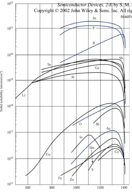
Precipitates of impurities or dopant atoms because of the inherent solubility of the impurity in the host lattice.The solubility of most impurities decreases with decreasing temperature.
If an impurity is introduced to the maximum
concentration allowed by its solubility and the crystal is then cooled, an equilibrium state is achieved by precipitating the impurity atoms in excess of the solubility level.
The volume mismatch between the host lattice and the precipitates results in dislocations.
Figure 10.18. Solid solubilities of impurity elements in silicon.11
Semiconductor Devices, 2/E by S. M. S Copyright © 2002 John Wiley & Sons. Inc. All righ
10/11/2004 Ettore Vittone- Fisica dei Semiconduttori - Lectio XIII 5
MATERIAL PROPERTIES:
Property Czochralski Float zone Requirements for ULSI
ρ (P) n-type (Ω⋅cm) 1-50 1-300 and up 4-40 and up
ρ(B) p-type (Ω⋅cm) 0.005-50 1-300 and up 4-40 and up
ρ gradient (%) 5-10 20 <1
τ(µs) 30-300 50-500 300-1000
Oxygen (ppma) 5-25 not detected
Carbon (ppma) 1-5 0.1-1 <0.1 Dislocation (per cm2) <500 <500 <1 Diameter (mm) up to 200 up to 100 up to 300 Slice bow (µm) <25 <25 <5 Slice taper (µm) <15 <15 <5 Surface flatness (µm) <5 <5 <1
Heavy metal impurity
(ppma) <1 <0.01 <0.001
1. Dissolution of oxygen from the silica crucible and transport of carbon to the melt from the graphite susceptor during crystal growth.
2. Carbon atoms in silicon occupy substitutional lattice sites. Formation of defects
3. Oxygen act as donor, distorting the resistivity -> unintentional doping
10/11/2004 Ettore Vittone- Fisica dei Semiconduttori - Lectio XIII 7
Figure 10.19.
Denuded zone width for two sets of processing conditions. Inset shows a schematic of the denuded zone and gettering
sites in a wafer cross section.1
Semiconductor Devices, 2/E by S. M. Sze Copyright © 2002 John Wiley & Sons. Inc. All rights
reserved.
Further thermal cycles to promote the formation of oxygen precipitates in the interior of the wafer for gettering impurities. Gettering thermal treatment oxygen evolution lowers the oxygen content at the surface (denuded zone). Figure 10.20.
Three common susceptors (graphite) for chemical vapor disposition
CVD (APCVD, LPCVD)
Mechanism of CVD:
• The reactants are transported to the substrate region
• Transfer to the substrate surface where they are absorbed
• A chemical reaction occurs,
catalyzed at the surface, followed by growth of the epitaxial layer
• The gaseous products are desorbed
into the main gas stream • The reaction products are
transported out of the reaction chamber Horizontal susceptor Pancake susceptor Barrel susceptor
10/11/2004 Ettore Vittone- Fisica dei Semiconduttori - Lectio XIII 9
Epitaxial growth
The substrate wafer acts as the seed crystal
Epitaxial layers can be grown at a temperature substantially below the melting point
Sources used for silicon CVD (or VPE) growth:
Silicon tetrachloride SiCl4 ; dichlorosilane SiH2Cl2 ; trichlorosilane SiHCl3 ; silane SiH4.
) gas ( SiCl 2 ) solid ( Si ) gas ( SiCl : reaction competing Additional ) gas ( HCl 4 ) solid ( Si ) gas ( H 2 ) gas ( SiCl : C) 1200 re (temperatu reaction Main 2 4 2 4 ↔ + + ↔ + ° ≈
If the SiCl4 concentration is too high, etching rather than growth of silicon will take part.
Figure 10.21. Effect of SiCl4
10/11/2004 Ettore Vittone- Fisica dei Semiconduttori - Lectio XIII 11 Sources used for silicon doping:
1. P-type: diborane (B2H6)
2. N-type: phosphine (PH3) and arsine (AsH3)
3. Diluent gas: hydrogen
4. High temperature are needed to give sufficient mobility to adsorbed atoms for finding their proper position
Semiconductor Devices, 2/E by S. M. Sze Copyright © 2002 John Wiley & Sons. Inc. All rights
reserved.
Figure 10.25. Schematic illustration of (a) lattice-matched, (b) strained, and (c) related heteroepitaxial structures.19 Homoepitaxy is structurally identical to the
lattice-matched heteroepitaxy.
Semiconductor Devices, 2/E by S. M. Sze Copyright © 2002 John Wiley & Sons. Inc. All rights
10/11/2004 Ettore Vittone- Fisica dei Semiconduttori - Lectio XIII 13
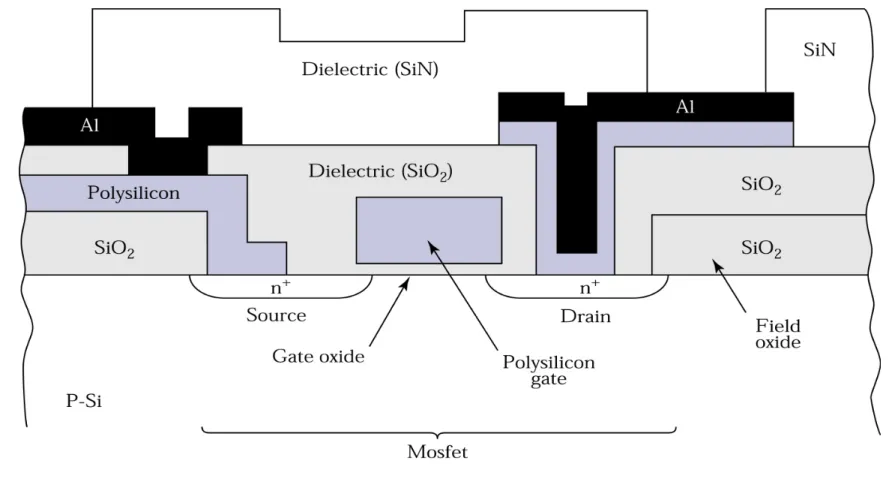
Figure 11.1. Schematic cross section of a metal-oxide-semiconductor field-effect transistor (MOSFET).
Figure 11.2. Schematic cross section of a resistance-heated oxidation furnace.
10/11/2004 Ettore Vittone- Fisica dei Semiconduttori - Lectio XIII 15
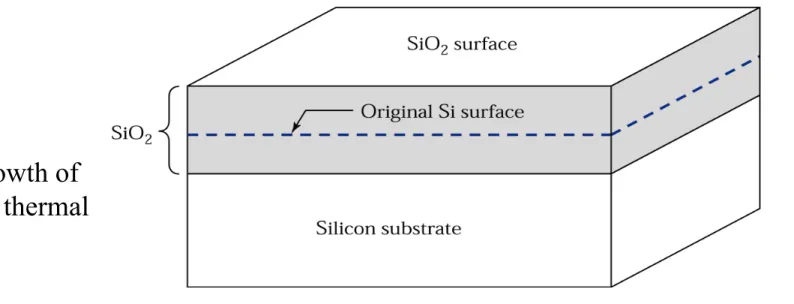
Figure 11.3. Growth of silicon dioxide by thermal
oxidation.
)
gas
(
H
2
)
solid
(
SiO
O
H
2
)
solid
(
Si
)
solid
(
SiO
)
gas
(
O
)
solid
(
Si
2 2 2 2 2+
→
+
→
+
For SiO2 thickness = 100 nm what is the Si thickness being consumed
ASi=28.9 g/mole ; ρSi=2.33 g/cm3
; ASiO2=60.8 g/mole ; ρSi=2.21 g/cm3;
Molar volume:
Vsi=28.9/2.33 cm3/mole =12.06 cm3/mole;
VsiO2=60.8/2.21 cm3/mole =27.18 cm3/mole;
1 mole of Si is converted in 1 mole of SiO2
44 0 18 27 06 12 . . . me) molar volu (SiO me) molar volu (Si ) thickness (SiO ) thickness (Si area x ) thickness (SiO area x ) thickness (Si 2 2 2 = = = =
10/11/2004 Ettore Vittone- Fisica dei Semiconduttori - Lectio XIII 17
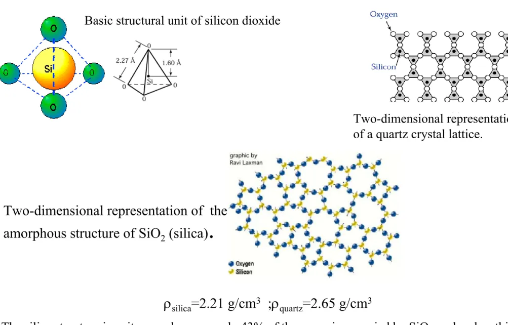
ρsilica=2.21 g/cm3 ;ρ
quartz=2.65 g/cm3
The silica structure is quite open because only 43% of the space is occupied by SiO2 molecules; this accounts for the lower density and allows impurities (e.g. Na) to enter and diffuse
Basic structural unit of silicon dioxide
Two-dimensional representation of the amorphous structure of SiO2 (silica)
.
Two-dimensional representation of a quartz crystal lattice.
Figure 11.5. Basic model for the thermal oxidation of silicon.2
− ⋅ τ + ⋅ ⋅ ⋅ + = 1 2 1 1 2 0 C D ) t ( k C k D x : thickness Oxide
C0=surface conc. of oxidants F1=flux of oxidants through SiO2 F2=flux of oxidants through Si C1=conc. Of oxidants in the oxide
As the oxide layer becomes thicker, the reaction becomes diffusion limited → ) t ( A B x= ⋅ +τ ) t ( B x = ⋅ +τ ) t ( A B x = ⋅ +τ
Early stages: x varies linearly with time; surface reaction is rate limiting
10/11/2004 Ettore Vittone- Fisica dei Semiconduttori - Lectio XIII 19
Figure 11.6.
Linear rate constant versus temperature.2
Figure 11.7.
Parabolic rate constant versus temperature.2
Thin oxide (gate oxide) → dry oxidation Thick oxide (field oxide) → wet oxidation
Dependence on crystal orientation
YE
S NO
Figure 11.8. Experimental results of silicon dioxide thickness as a function of
reaction time and temperature for two substrate orientations. (a) Growth in dry oxygen. (b)
10/11/2004 Ettore Vittone- Fisica dei Semiconduttori - Lectio XIII 21
Dielectric Deposition
Dielectric Deposition
Used mainly for insulation and passivation of discrete devices.
Hot-wall, reduced-pressure reactor. (LPCVD)
Parallel-plate plasma
deposition reactor.4 rf, radio
frequency. (PECVD)
Low deposition temperature Limited capacity
Semiconductor Devices, 2/E by S. M. Sze Copyright © 2002 John Wiley & Sons. Inc. All rights reserved.
The best dielectric properties are obtained with thermally grown films CVD oxides are used instead to complement the thermal oxides.
A layer of undoped silicon dioxide is used
To insulate multilever metallisation To mask ion implant or diffusion
To increase the thickness of thermally grown field oxides.
10/11/2004 Ettore Vittone- Fisica dei Semiconduttori - Lectio XIII 23
Low temperature deposition (300-500°C)
2 2 C 450 2 4
O
SiO
2
H
SiH
+
→
°+
Both at atmospheric pressure or at low pressure (LPCVD)
The low temperature allows the deposition of SiO2 on Al
Intermediate temperature deposition (500-800°C)
products
-by
SiO
O
)
H
OC
(
Si
2 5 4+
2
→
700
°C 2+
Low pressure (LPCVD) decomposition of TEOS (tetraethylorthosilicate) vaporized from a liquid source.
No suitable to cover Al. Suitable for polysilicon gates requiring a uniform insulating layer due to an enhance surface mobility at high temperature
SiO
SiO
2
2
Properties of SiO
2films
Property Thermally grown SiH4+O2 TEOS
@1000°C @450°C @700°C
Composition SiO2 SiO2(H) SiO2
Density (g/cm3) 2.2 2.1 2.2
Refractive index(628 nm)1.46 1.44 1.46
Dielectric strength >107V/cm 8·106V/cm 107V/cm Etch rate (100:1 H20:HF)3 nm/min 6 nm/min 3 nm/min
Low density → films deposited below 500°C
SiO
10/11/2004 Ettore Vittone- Fisica dei Semiconduttori - Lectio XIII 25
Figure 11.12.
Step coverage of deposited films. (a) Conformal step coverage. (b) Nonconformal step coverage.4
The uniformity of the film thickness, regardless to the topography is due to the rapid micgration of reactants after adsorption on the step surface. TEOS gives a nearly conformal coverage.
Semiconductor Devices, 2/E by S. M. Sze Copyright © 2002 John Wiley & Sons. Inc. All rights
reserved.
SiO
SiO
2
2
Silicon Nitride
Silicon Nitride
LPCVD – High temperature (750°C) –Stoichiometric composition Si3N4, High density (2.9-3.1 g/cm3)
Are used to passivate devices because they serve as a good barrier to the diffusion of water or sodium.
Used as masks for selective oxidation of Si because oxidation is very slow. Because of the low pressure →good film uniformity
2 4 3 C 750 3 2 2
H
4
NH
Si
N
6
HCl
6
H
SiCl
3
+
→
°+
+
Silicon Nitride deposited by LPCVD is an amorphous dielectric containing up to 8 atomic percent of H.
Etch rate is less than 1 nm/min
10/11/2004 Ettore Vittone- Fisica dei Semiconduttori - Lectio XIII 27
PECVD – Low temperature (300°C) –
Non stoichiometric composition Low density (2.4-2.8 g/cm3)
Because of the low temperature deposition,is used over fabricated devices for final passivation. Excellent scratch protection, moisture barrier and prevents sodium diffusion.
Silicon Nitride
Silicon Nitride
2 discharge N in C 300 2 4 2 plasma Ar in C 300 3 4H
3
SiNH
2
N
SiH
2
H
3
SiNH
NH
SiH
2
+
→
+
+
→
+
° °The products are strongly dependent on deposition conditions.
Large H concentration (20-25%), film resistivities from 105 to 1021 Ω⋅cm, dielectric
strength from 106 to 6x10⁶ V/cm.
Low dielectric constant materials
As devices continue to scale down to the deep submicron region, they require multilevel interconnection architecture to minimize the time delay due to parasitic resistance and capacitance .
Long interconnections-propagation delay due to RC
To reduce RC time constant of ULSI circuitis,inteconnection materials with low resistivity and interlayer films with low capacitance are
required
To reduce parasitic capacitance
Increasing thickness of interlayer dielectric →gap filling difficult
Decreasing wiring height and area →increase of interconnect resistance
10/11/2004 Ettore Vittone- Fisica dei Semiconduttori - Lectio XIII 29
Estimate the intrinsic RC value of two parallel Al wires A=0.5 µm x0.5 µm,
L=1mm and separated by a dielectric layer 0.5 µm thick. Al resistivity is 2.7
µΩ⋅cm. (ps) 96 . 0 10 5 1 . 0 10 5 10 85 . 8 10 25 1 . 0 10 7 . 2 t L y y x L RC 5 5 14 10 6 0 ε ⋅ = = ε ⋅ ⋅ ⋅ ⋅ ⋅ ⋅ ⋅ ⋅ ⋅ ⋅ = ε⋅ε ⋅ ⋅ ⋅ ⋅ ⋅ ρ = − − − − − x=0.5 µm y= 0.5 µ m L=1 mm t=0.5 µm Dielectric ε Si3N4 7 Black diamond 2.7-3 Teflon 1.93 Fluorosilicate glass 3.5-4.0 Figure 11.14.
Calculated gate and interconnect delay versus technology generation. The dielectric constant for the low-k material is 2.0.
Both Al and Cu are 0.8
µm thick and 43 µm long.
Semiconductor Devices, 2/E by S. M. Sze Copyright © 2002 John Wiley & Sons. Inc. All rights
10/11/2004 Ettore Vittone- Fisica dei Semiconduttori - Lectio XIII 31
High dielectric constant materials
Required for dynamic random access memory (DRAM).The storage capacitor in a DRAM has to maintain a certain value of capacitance for proper operation (40 fF).
C = ε⋅ε0 ⋅ A/d → The dielectric constant of the film must be increased.
Barium strontium titanate (BST) ε =300-500
Lead zirconium titanate (PZT) ε >1000
Tantalum oxide (Ta2O5) ε =25
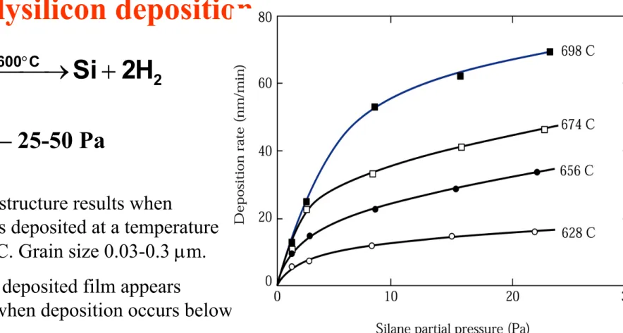
Polysilicon deposition
Electrode reliability: the inferior time to breakdown of Al electrode is due to the migration of Al into the Thin oxide under the electrical fieldFigure 11.15.
Maximum time to breakdown versus oxide thickness for a polysilicon electrode and an
aluminum electrode.10
Why polysilicon ?
Polysilicon is used as a diffusion source to create shallow junctions Polysilicon is used to ensure ohmic contact to crystalline silicon
10/11/2004 Ettore Vittone- Fisica dei Semiconduttori - Lectio XIII 33 2 C 600 4
Si
2
H
SiH
→
°+
Polysilicon deposition
LPCVD – 25-50 PaA columnar structure results when
polysilicon is deposited at a temperature of 600-650°C. Grain size 0.03-0.3 µm. The initially deposited film appears
amorphous when deposition occurs below 600°C
Figure 11.16. Effect of silane concentration on the polysilicon deposition rate.4
Metallization
Physical vapor deposition: evaporations occus when a source of meaterial is heated above its melting point in an evacuated chamber.
The source can be molten by resistance heating, by rf heating or with a focused electron beam.
In ion beam sputtering a source of ions is accelerated toward the target and impinged on its surface. The sputtered material deposits on a wafer that is placed facing the target.
To increase the sputter deposition rate, a third electrode is used which
provides more electrons for ionisation or to use a magnetic field (ECR) to capture and spiral electrons, increasing their ionising efficiency in vicinity