Low-Power SoC (System-on-Chip) with MCU, Memory,
2.4 GHz RF Transceiver, and USB Controller
Applications
• 2400 - 2483.5 MHz ISM/SRD band systems
• Consumer electronics
• Wireless keyboard and mouse
• Wireless voice-quality audio
• RF enabled remote controls
• Wireless sports and leisure equipment
• Low power telemetry
• CC2511Fx: USB dongles
Product Description
The CC2510Fx/CC2511Fx is a true low-cost 2.4 GHz system-on-chip (SoC) designed for low-power wireless applications. The
CC2510Fx/CC2511Fx combines the excellent
performance of the state-of-the-art RF transceiver CC2500 with an industry-standard enhanced 8051 MCU, up to 32 kB of in-system programmable flash memory and 4 kB of RAM, and many other powerful features. The small 6x6 mm package makes it very suited for applications with size limitations.
The CC2510Fx/CC2511Fx is highly suited for
systems where very low power consumption is required. This is ensured by several advanced low-power operating modes. The CC2511Fx adds a full-speed USB controller to the feature set of the CC2510Fx. Interfacing to a PC using the USB interface is quick and easy, and the high data rate (12 Mbps) of the USB interface avoids the bottlenecks of RS-232 or low-speed USB interfaces.
Key Features
• Radioo High-performance RF transceiver based on the market-leading CC2500
o Excellent receiver selectivity and blocking performance
o High sensitivity (−103 dBm at 2.4 kBaud) o Programmable data rate up to 500 kBaud o Programmable output power up to 1 dBm for
all supported frequencies
o Frequency range: 2400 - 2483.5 MHz o Digital RSSI / LQI support
• Current Consumption
o Low current consumption (RX: 17.1 mA @ 2.4 kBaud, TX: 16 mA @ −6 dBm output power)
o 0.3 µA in PM3 (the operating mode with the lowest power consumption)
• MCU, Memory, and Peripherals
o High performance and low power 8051 microcontroller core.
o 8/16/32 kB in-system programmable flash, and 1/2/4 kB RAM
o Full-Speed USB Controller with 1 kB USB FIFO (CC2511Fx )
o I2S interface
o 7 - 12 bit ADC with up to eight inputs o 128-bit AES security coprocessor o Powerful DMA functionality o Two USARTs
o 16-bit timer with DSM mode o Three 8-bit timers
o Hardware debug support
o 21 (CC2510Fx ) or 19 (CC2511Fx ) GPIO pins • General
Table of Contents
ABBREVIATIONS ... 4
1 REGISTER CONVENTIONS ... 5
2 KEY FEATURES (IN MORE DETAILS) ... 6
2.1 HIGH-PERFORMANCE AND LOW-POWER 8051-COMPATIBLE MICROCONTROLLER... 6
2.2 8/16/32 KB NON-VOLATILE PROGRAM MEMORY AND 1/2/4 KB DATA MEMORY ... 6
2.3 FULL-SPEED USB CONTROLLER (CC2511FX ) ... 6
2.4 I2S INTERFACE ... 6
2.5 HARDWARE AES ENCRYPTION/DECRYPTION ... 6
2.6 PERIPHERAL FEATURES ... 6
2.7 LOW POWER ... 6
2.8 2.4 GHZ RADIO WITH BASEBAND MODEM ... 7
3 ABSOLUTE MAXIMUM RATINGS ... 8
4 OPERATING CONDITIONS ... 9 4.1 CC2510FX OPERATING CONDITIONS ... 9 4.2 CC2511FX OPERATING CONDITIONS ... 9 5 GENERAL CHARACTERISTICS ... 9 6 ELECTRICAL SPECIFICATIONS ... 10 6.1 CURRENT CONSUMPTION ... 10 6.2 RF RECEIVE SECTION ... 13 6.3 RF TRANSMIT SECTION ... 15 6.4 CRYSTAL OSCILLATORS ... 16 6.5 32.768 KHZ CRYSTAL OSCILLATOR ... 17
6.6 LOW POWER RC OSCILLATOR ... 17
6.7 HIGH SPEED RC OSCILLATOR ... 18
6.8 FREQUENCY SYNTHESIZER CHARACTERISTICS ... 18
6.9 ANALOG TEMPERATURE SENSOR ... 19
6.10 7 - 12 BIT ADC ... 20
6.11 CONTROL AC CHARACTERISTICS ... 22
6.12 SPI AC CHARACTERISTICS ... 23
6.13 DEBUG INTERFACE AC CHARACTERISTICS ... 24
6.14 PORT OUTPUTS AC CHARACTERISTICS ... 24
6.15 TIMER INPUTS AC CHARACTERISTICS ... 25
6.16 DC CHARACTERISTICS ... 25
7 PIN AND I/O PORT CONFIGURATION ... 26
8 CIRCUIT DESCRIPTION ... 30
8.1 CPU AND PERIPHERALS ... 31
8.2 RADIO ... 33
9 APPLICATION CIRCUIT ... 33
9.1 BIAS RESISTOR ... 33
9.2 BALUN AND RF MATCHING ... 33
9.3 CRYSTAL ... 33
9.4 REFERENCE SIGNAL ... 34
9.5 USB (CC2511FX) ... 34
9.6 POWER SUPPLY DECOUPLING ... 34
9.7 PCB LAYOUT RECOMMENDATIONS ... 38
10 8051 CPU ... 39
10.1 8051 INTRODUCTION ... 39
10.2 MEMORY ... 39
10.3 CPU REGISTERS ... 51
10.4 INSTRUCTION SET SUMMARY ... 53
10.5 INTERRUPTS ... 57
11 DEBUG INTERFACE ... 68
11.1 DEBUG MODE ... 68
11.2 DEBUG COMMUNICATION... 68
11.4 DEBUG COMMANDS... 69
12 PERIPHERALS ... 73
12.1 POWER MANAGEMENT AND CLOCKS... 73
12.2 RESET ... 80
12.3 FLASH CONTROLLER ... 81
12.4 I/O PORTS ... 87
12.5 DMA CONTROLLER ... 98
12.6 16-BIT TIMER, TIMER 1 ... 109
12.7 MAC TIMER (TIMER 2) ... 121
12.8 SLEEP TIMER ... 123
12.9 8-BIT TIMERS, TIMER 3 AND TIMER 4 ... 126
12.10 ADC ... 137
12.11 RANDOM NUMBER GENERATOR ... 143
12.12 AES COPROCESSOR ... 144 12.13 WATCHDOG TIMER ... 147 12.14 USART ... 149 12.15 I2S ... 159 12.16 USB CONTROLLER ... 167 13 RADIO ... 183 13.1 COMMAND STROBES ... 183 13.2 RADIO REGISTERS ... 185 13.3 INTERRUPTS ... 185 13.4 TX/RX DATA TRANSFER ... 187
13.5 DATA RATE PROGRAMMING ... 188
13.6 RECEIVER CHANNEL FILTER BANDWIDTH ... 188
13.7 DEMODULATOR, SYMBOL SYNCHRONIZER, AND DATA DECISION ... 189
13.8 PACKET HANDLING HARDWARE SUPPORT ... 190
13.9 MODULATION FORMATS ... 193
13.10 RECEIVED SIGNAL QUALIFIERS AND LINK QUALITY INFORMATION ... 194
13.11 FORWARD ERROR CORRECTION WITH INTERLEAVING ... 197
13.12 RADIO CONTROL ... 198
13.13 FREQUENCY PROGRAMMING ... 201
13.14 VCO ... 202
13.15 OUTPUT POWER PROGRAMMING ... 202
13.16 SELECTIVITY ... 203
13.17 SYSTEM CONSIDERATIONS AND GUIDELINES ... 205
13.18 RADIO REGISTERS ... 208
14 VOLTAGE REGULATORS ... 226
14.1 VOLTAGE REGULATOR POWER-ON ... 226
15 RADIO TEST OUTPUT SIGNALS ... 226
16 REGISTER OVERVIEW ... 228
17 REFERENCES ... 232
18 GENERAL INFORMATION ... 233
Abbreviations
∆Σ Delta-Sigma
ADC Analog to Digital Converter AES Advanced Encryption Standard AGC Automatic Gain Control
ARIB Association of Radio Industries and Businesses
BCD Binary Coded Decimal BER Bit Error Rate BOD Brown Out Detector CBC Cipher Block Chaining
CBC-MAC
Cipher Block Chaining Message Authentication Code
CCA Clear Channel Assessment CCM Counter mode + CBC-MAC CFB Cipher Feedback
CFR Code of Federal Regulations CMOS Complementary Metal Oxide
Semiconductor CPU Central Processing Unit CRC Cyclic Redundancy Check CTR Counter mode (encryption) DAC Digital to Analog Converter DMA Direct Memory Access DSM Delta-Sigma Modulator ECB Electronic Code Book EM Evaluation Module ENOB Effective Number of Bits EP{0 - 5} USB Endpoints 0 - 5 ESD Electro Static Discharge ESR Equivalent Series Resistance
ETSI European Telecommunications Standard Institute
FCC Federal Communications Commission FIFO First In First Out
GPIO General Purpose Input / Output HSSD High Speed Serial Debug HW Hardware
I2S Inter-IC Sound I/O Input / Output
I/Q In-phase / Quadrature-phase IF Intermediate Frequency IOC I/O Controller
ISM Industrial, Scientific and Medical ISR Interrupt Service Routine IV Initialization Vector
JEDEC Joint Electron Device Engineering Council kbps kilo bits per second
KB Kilo Bytes (1024 bytes) LFSR Linear Feedback Shift Register
LNA Low-Noise Amplifier LO Local Oscillator LQI Link Quality Indication LSB Least Significant Bit / Byte MAC Medium Access Control MCU Microcontroller Unit MISO Master In Slave Out MOSI Master Out Slave In MSB Most Significant Bit / Byte NA Not Applicable
OFB Output Feedback (encryption) PA Power Amplifier
PCB Printed Circuit Board PER Packet Error Rate PLL Phase Locked Loop PM{0 - 3} Power Mode 0 - 3
PMC Power Management Controller POR Power On Reset
PWM Pulse Width Modulator
Px_n Port x pin n (x = 0, 1, or 2 and n = 0, 1, 2, .., 7)
QLP Quad Leadless Package RAM Random Access Memory RCOSC RC Oscillator
RF Radio Frequency
RoHS Restriction on Hazardous Substances RSSI Receive Signal Strength Indicator RX Receive
SCK Serial Clock
SFD Start of Frame Delimiter SFR Special Function Register SINAD Signal-to-noise and distortion ratio SPI Serial Peripheral Interface SRAM Static Random Access Memory SW Software
T/R Transmit / Receive TX Transmit
UART Universal Asynchronous Receiver/Transmitter
USART Universal Synchronous/Asynchronous Receiver/Transmitter
USB Universal Serial Bus VCO Voltage Controlled Oscillator VGA Variable Gain Amplifier WDT Watchdog Timer XOSC Crystal Oscillator
1
Register Conventions
Each SFR is described in a separate table. The table heading is given in the following format:
REGISTER NAME (SFR Address) - Register Description.
Each RF register is described in a separate table. The table heading is given in the following format:
XDATA Address: REGISTER NAME - Register Description
All register descriptions include a symbol denoted R/W describing the accessibility of each bit in the register. The register values are always given in binary notation unless prefixed by ‘0x’, which indicates hexadecimal notation.
Symbol Access Mode R/W Read/write R Read only R0 Read as 0 R1 Read as 1 W Write only W0 Write as 0 W1 Write as 1 H0 Hardware clear H1 Hardware set
2
Key Features (in more details)
2.1 High-Performance and Low-Power 8051-Compatible Microcontroller
• Optimized 8051 core which typically gives 8x the performance of a standard 8051
• Two data pointers
• In-circuit interactive debugging is supported by the IAR Embedded Workbench through a simple two-wire serial interface
• SW compatible with CC1110Fx/CC1111Fx
2.2 8/16/32 kB Non-volatile Program Memory and 1/2/4 kB Data Memory
• 8, 16, or 32 kB of non-volatile flash memory, in-system programmable through a simple two-wire interface or by the 8051 core
• Minimum flash memory endurance: 1000 write/erase cycles
• Programmable read and write lock of portions of flash memory for software security
• 1, 2, or 4 kB of internal SRAM
2.3 Full-Speed USB Controller (CC2511Fx )
• 5 bi-directional endpoints in addition to control endpoint 0
• Full-Speed, 12 Mbps transfer rate • Support for Bulk, Interrupt, and
Isochronous endpoints
• 1024 bytes of dedicated endpoint FIFO memory
• 8 - 512 byte data packet size supported • Configurable FIFO size for IN and OUT
direction of endpoint
2.4 I2S Interface
• Industry standard I2S interface for transfer of digital audio data
• Full duplex
• Mono and stereo support
• Configurable sample rate and sample size
• Support for µ-law compression and expansion
• Typically used to connect to external DAC or ADC
2.5 Hardware AES Encryption/Decryption
• 128-bit AES supported in hardware coprocessor
2.6 Peripheral Features
• Powerful DMA Controller
• Power On Reset/Brown-Out Detection • ADC with eight individual input
channels, single-ended or differential
(CC2511Fx has six channels) and
configurable resolution
• Programmable watchdog timer
• Five timers: one general 16-bit timer with DSM mode, two general 8-bit timers, one MAC timer, and one sleep timer
• Two programmable USARTs for master/slave SPI or UART operation • 21 configurable general-purpose digital
I/O-pins (CC2511Fx has 19) • Random number generator
2.7 Low Power
• Four flexible power modes for reduced power consumption
• System can wake up on external interrupt or when the Sleep Timer expires
• 0.5 µA current consumption in PM2, where external interrupts or the Sleep Timer can wake up the system
• 0.3 µA current consumption in PM3, where external interrupts can wake up the system
• Low-power fully static CMOS design • System clock source is either a high
speed crystal oscillator (24 - 27 MHz for
CC2510Fx and 48 MHz for CC2511Fx) or a high speed RC oscillator (12 - 13.5 MHz for CC2510Fx and 12 MHz for CC2511Fx).
The high speed crystal oscillator must be used when the radio is active.
• Clock source for ultra-low power operation can be either a low-power RC oscillator or an optional 32.768 kHz crystal oscillator
• Very fast transition to active mode from power modes enables ultra low average power consumption in low duty-cycle systems
2.8 2.4 GHz Radio with Baseband Modem
• Based on the industry leading CC2500 radio core
• Few external components: On-chip frequency synthesizer, no external filters or RF switch needed
• Flexible support for packet oriented systems: On-chip support for sync word detection, address check, flexible packet length, and automatic CRC handling
• Supports use of DMA for both RX and TX resulting in minimal CPU intervention even on high data rates • Programmable channel filter bandwidth
• 2-FSK, GFSK and MSK supported • Optional automatic whitening and
de-whitening of data
• Programmable Carrier Sense (CS) indicator
• Programmable Preamble Quality Indicator for detecting preambles and improved protection against sync word detection in random noise
• Support for automatic Clear Channel Assessment (CCA) before transmitting (for listen-before-talk systems
• Support for per-package Link Quality Indication (LQI)
• Suited for systems targeting compliance with EN 300 328, EN 300 440, FCC CFR47 Part 15 and ARIB STD-T-66 • When transmitting in band 2480 -
2483.5 MHz under FCC, duty-cycling or reducing output power might be needed
3
Absolute Maximum Ratings
Under no circumstances must the absolute maximum ratings given in Table 2 be violated. Stress exceeding one or more of the limiting values may cause permanent damage to the device.
Parameter Min Max Units Condition
Supply voltage (VDD) −0.3 3.9 V All supply pins must have the same voltage Voltage on any digital pin −0.3 VDD + 0.3,
max 3.9 V Voltage on the pins RF_P, RF_N
and DCOUPL
−0.3 2.0 V Voltage ramp-up rate 120 kV/µs
Input RF level 10 dBm
Storage temperature range −50 150 °C Device not programmed
Solder reflow temperature 260 °C According to IPC/JEDEC J-STD-020D
ESD CC2510Fx 750 V According to JEDEC STD 22, method A114, Human Body Model (HBM)
ESD CC2510Fx 500 V According to JEDEC STD 22, C101C, Charged Device Model (CDM)
ESD CC2511x 750 V According to JEDEC STD 22, method A114, Human Body Model (HBM)
ESD CC2511x 500 V According to JEDEC STD 22, C101C, Charged Device Model (CDM)
Table 2: Absolute Maximum Ratings
Caution! ESD sensitive device. Precaution should be used when handling the device in order to prevent permanent damage.
4
Operating Conditions
4.1 CC2510Fx Operating Conditions
The operating conditions for CC2510Fx are listed in Table 3 below. Parameter Min Max Unit Condition Operating ambient temperature, TA −40 85 °C
Operating supply voltage (VDD) 2.0 3.6 V All supply pins must have the same voltage
Table 3: Operating Conditions for CC2510Fx
4.2 CC2511Fx Operating Conditions
The operating conditions for CC2511Fx are listed in Table 4 below. Parameter Min Max Unit Condition Operating ambient temperature, TA 0 85 °C
Operating supply voltage (VDD) 3.0 3.6 V All supply pins must have the same voltage
Table 4: Operating Conditions for CC2511Fx
5
General Characteristics
TA = 25°C, VDD = 3.0 V if nothing else stated
Parameter Min Typ Max Unit Condition/Note Radio part
Frequency range 2400 2483.5 MHz There will be spurious signals at n/2·crystal oscillator frequency (n is an integer number). RF frequencies at n/2·crystal oscillator frequency should therefore be avoided (e.g. 2405, 2418, 2431, 2444, 2457, 2470 and 2483 MHz when using a 26 MHz crystal).
Data rate 1.2 1.2 26 500 250 500 kBaud kBaud kBaud 2-FSK GFSK
(Shaped) MSK (also known as differential offset QPSK) Optional Manchester encoding (the data rate in kbps will be half the baud rate)
Wake-Up Timing PM1 Active Mode
4 µs Digital regulator on. HS RCOSC and high speed crystal oscillator off. 32.768 kHz XOSC or low power RCOSC running.
SLEEP.OSC_PD=1 and CLKCON.OSC=1
PM2/3 Active Mode
100 µs Digital regulator off. HS RCOSC and high speed crystal oscillator off. 32.768 kHz XOSC or low power RCOSC running (PM2). No crystal oscillators or RC oscillators are running in PM3.
SLEEP.OSC_PD=1 and CLKCON.OSC=1
6
Electrical Specifications
6.1 Current Consumption
TA = 25°C, VDD = 3.0 V if nothing else stated. All measurement results are obtained using the CC2510EM reference design ([1]).
Parameter Min Typ Max Unit Condition Active mode, full
speed (high speed crystal oscillator)1. Low CPU activity.
4.8 mA System clock running at 26 MHz. 4.6 mA System clock running at 24 MHz.
Digital regulator on. High speed crystal oscillator and low power RCOSC running. No peripherals running.
Low CPU activity: No flash access (i.e. only cache hit), no RAM access
Active mode, full speed (HS RCOSC)1. Low CPU activity.
2.5 mA System clock running at 13 MHz.
Digital regulator on. HS RCOSC and low power RCOSC running. No peripherals running.
Low CPU activity: No flash access (i.e. only cache hit), no RAM access
Active mode with radio in RX
Digital regulator on. High speed crystal oscillator and low power RCOSC running. Radio in RX mode (sensitivity optimized
MDMCFG2.DEM_DCFILT_OFF=0) 19.8 20.6 17.1 mA mA mA
2.4 kBaud, input at sensitivity limit, system clock running at 26 MHz. 2.4 kBaud, input at sensitivity limit, system clock running at 24 MHz. 2.4 kBaud, input at sensitivity limit, system clock running at 203 kHz. 19.8 mA 2.4 kBaud, input well above sensitivity limit, system clock running at
26 MHz. 21.5 22.1 18.8 mA mA mA
10 kBaud, input at sensitivity limit, system clock running at 26 MHz. 10 kBaud, input at sensitivity limit, system clock running at 24 MHz. 10 kBaud, input at sensitivity limit, system clock running at 203 kHz. 19.0 mA 10 kBaud, input well above sensitivity limit, system clock running at
26 MHz. 22.9 22.7 20.5 mA mA mA
250 kBaud, input at sensitivity limit, system clock running at 26 MHz. 250 kBaud, input at sensitivity limit, system clock running at 24 MHz. 250 kBaud, input at sensitivity limit, system clock running at 1.625 MHz.
19.6 mA 250 kBaud, input well above sensitivity limit, system clock running at 26 MHz. See Figure 2 for typical variation over operating conditions 19.7 20.8 17.5 mA mA mA
500 kBaud, input at sensitivity limit, system clock running at 26 MHz. 500 kBaud, input at sensitivity limit, system clock running at 24 MHz. 500 kBaud, input at sensitivity limit, system clock running at 3.25 MHz.
16.7 mA 500 kBaud, input well above sensitivity limit
Digital regulator on. High speed crystal oscillator and low power RCOSC running. Radio in RX mode (current optimized
MDMCFG2.DEM_DCFILT_OFF=1)
17.4 mA 2.4 kBaud, input at sensitivity limit, system clock running at 26 MHz. 14.7 mA 2.4 kBaud, input at sensitivity limit, system clock running at 203 kHz. 17.4 mA 2.4 kBaud, input well above sensitivity limit, system clock running at
26 MHz.
1
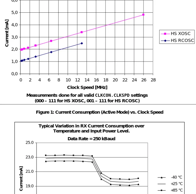
Note: In order to reduce the current consumption in active mode, the clock speed can be reduced by setting CLKCON.CLKSPD≠000 (see section 13.1 for details). Figure 1 shows typical current consumption in active mode for different clock speeds
Parameter Min Typ Max Unit Condition
19.4 mA 10 kBaud, input at sensitivity limit, system clock running at 26 MHz. 15.7 mA 10 kBaud, input at sensitivity limit, system clock running at 203 kHz. 16.9 mA 10 kBaud, input well above sensitivity limit, system clock running at
26 MHz. Active mode with
radio in TX
System clock running at 26 MHz.
Digital regulator on. High speed crystal oscillator and low power RCOSC running. Radio in TX mode
26 mA 0 dBm output power (PA_TABLE0=0xFE). See Table 7 for typical variation over operating conditions
18.5 mA −6 dBm output power (PA_TABLE0=0x7F) 15.5 mA −12 dBm output power (PA_TABLE0=0x95)
26 mA System clock running at 24 MHz.
Digital regulator on. High speed crystal oscillator and low power RCOSC running. Radio in TX mode w/0 dBm output power (PA_TABLE0=0xFE)
PM0 4.3 mA Same as active mode, but the CPU is not running (see 12.1.2.2 for details). System clock running at 26 MHz
PM1 220 µA Digital regulator on. HS RCOSC and high speed crystal oscillator off. 32.768 kHz XOSC or low power RCOSC running (see 12.1.2.3 for details)
PM2 0.5 1 µA Digital regulator off. HS RCOSC and high speed crystal oscillator off. Low power RCOSC running (see 12.1.2.4 for details)
PM3 0.3 1 µA Digital regulator off. No crystal oscillators or RC oscillators are running (see 12.1.2.5 for details)
Peripheral Current Consumption
Add to the figures above if the peripheral unit is activated
Timer 1 2.7 µA/MHz When running Timer 2 1.3 µA/MHz When running Timer 3 1.6 µA/MHz When running Timer 4 2 µA/MHz When running
ADC 1.2 mA During conversion
Figure 1: Current Consumption (Active Mode) vs. Clock Speed
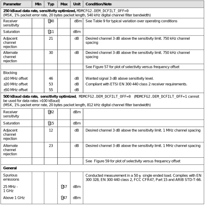
Figure 2:Typical Variation in RX Current Consumption over Temperature and Input Power Level. Data Rate = 250 kBaud.
Supply Voltage, VDD = 2 V Supply Voltage, VDD = 3 V Supply Voltage, VDD = 3.6 V Temperature [°C] −40 25 85 −40 25 85 −40 25 85 Current [mA] 26 25.6 26 26.3 26 26.3 26.5 26.2 26.6
Table 7: Typical Variation in TX Current Consumption over Temperature and Supply Voltage, 0 dBm Output Power
Typical Variation in RX Current Consumption over Temperature and Input Power Level.
Data Rate = 250 kBaud
15.0 17.0 19.0 21.0 23.0 25.0 -120 -100 -80 -60 -40 -20 0
Input Power Level [dBm]
Cu rre n t [ m A ] -40 °C +25 °C +85 °C
Current Consumption Active Mode. No Peripherals Running.
fxosc = 26 MHz 0,0 1,0 2,0 3,0 4,0 5,0 6,0 0 2 4 6 8 10 12 14 16 18 20 22 24 26 28 Clock Speed [MHz]
Measurements done for all valid CLKCON.CLKSPD settings (000 – 111 for HS XOSC, 001 – 111 for HS RCOSC)
C u rr e n t [m A ] HS XOSC HS RCOSC
6.2 RF Receive Section
TA = 25°C, VDD = 3.0 V if nothing else stated. All measurement results are obtained using the CC2510EM reference design ([1]).
Parameter Min Typ Max Unit Condition/Note Digital channel
filter bandwidth
58 812 kHz User programmable (see Section 13.6). The bandwidth limits are proportional to crystal frequency (given values assume a 26.0 MHz crystal).
2.4 kBaud data rate, sensitivity optimized,MDMCFG2.DEM_DCFILT_OFF=0
(2-FSK, 1% packet error rate, 20 bytes packet length, 203 kHz digital channel filter bandwidth) Receiver
sensitivity
−103 dBm The RX current consumption can be reduced by approximately 2.4 mA by setting MDMCFG2.DEM_DCFILT_OFF=1. The typical sensitivity is then −101 dBm.
The sensitivity can be improved to typically −105 dBm with
MDMCFG2.DEM_DCFILT_OFF=0 by changing registers TEST2 and
TEST1 (see Page 222). The temperature range is then from 0oC to 85oC.
Saturation −10 dBm
Adjacent channel rejection
23 dB Desired channel 3 dB above the sensitivity limit. 250 kHz channel spacing
Alternate channel rejection
32 dB Desired channel 3 dB above the sensitivity limit. 250 kHz channel spacing
See Figure 55 for plot of selectivity versus frequency offset Blocking ±10 MHz offset ±20 MHz offset ±50 MHz offset 64 70 71 dB dB dB
Wanted signal 3 dB above sensitivity level.
Compliant with ETSI EN 300 440 class 2 receiver requirements. 10 kBaud data rate, sensitivity optimized, MDMCFG2.DEM_DCFILT_OFF=0
(2-FSK, 1% packet error rate, 20 bytes packet length, 232 kHz digital channel filter bandwidth) Receiver
sensitivity
−98 dBm The RX current consumption can be reduced by approximately 2.2 mA by setting MDMCFG2.DEM_DCFILT_OFF=1. The typical sensitivity is then −97 dBm.
The sensitivity can be improved to typically −100 dBm with
MDMCFG2.DEM_DCFILT_OFF=0 by changing registers TEST2 and
TEST1 (see Page 222). The temperature range is then from 0oC to 85oC.
Saturation −9 dBm
Adjacent channel rejection
19 dB Desired channel 3 dB above the sensitivity limit. 250 kHz channel spacing
Alternate channel rejection
25 dB Desired channel 3 dB above the sensitivity limit. 250 kHz channel spacing
See Figure 56 for plot of selectivity versus frequency offset Blocking ±10 MHz offset ±20 MHz offset ±50 MHz offset 59 65 66 dB dB dB
Wanted signal 3 dB above sensitivity level.
Parameter Min Typ Max Unit Condition/Note
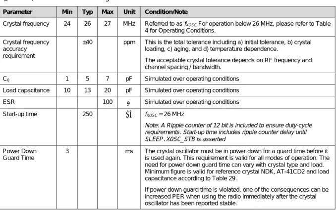
250 kBaud data rate, sensitivity optimized,MDMCFG2.DEM_DCFILT_OFF=0
(MSK, 1% packet error rate, 20 bytes packet length, 540 kHz digital channel filter bandwidth) Receiver
sensitivity
−90 dBm See Table 9 for typical variation over operating conditions
Saturation −11 dBm
Adjacent channel rejection
21 dB Desired channel 3 dB above the sensitivity limit. 750 kHz channel spacing
Alternate channel rejection
30 dB Desired channel 3 dB above the sensitivity limit. 750 kHz channel spacing
See Figure 57 for plot of selectivity versus frequency offset Blocking ±10 MHz offset ±20 MHz offset ±50 MHz offset 46 53 55 dB dB dB
Wanted signal 3 dB above sensitivity level.
Compliant with ETSI EN 300 440 class 2 receiver requirements. 500 kBaud data rate, sensitivity optimized, MDMCFG2.DEM_DCFILT_OFF=0 (MDMCFG2.DEM_DCFILT_OFF=1 cannot be used for data rates >100 kBaud)
(MSK, 1% packet error rate, 20 bytes packet length, 812 kHz digital channel filter bandwidth) Receiver sensitivity −82 dBm Saturation −15 dBm Adjacent channel rejection
12 dB Desired channel 3 dB above the sensitivity limit. 1 MHz channel spacing
Alternate channel rejection
23 dB Desired channel 3 dB above the sensitivity limit. 1 MHz channel spacing
See Figure 59 for plot of selectivity versus frequency offset General
Spurious emissions
Conducted measurement in a 50 Ω single ended load. Complies with EN 300 328, EN 300 440 class 2, FCC CFR47, Part 15 and ARIB STD-T-66. 25 MHz -
1 GHz
−57 dBm
Above 1 GHz −47 dBm
Table 8: RF Receive Section
Supply Voltage, VDD = 2 V Supply Voltage, VDD = 3 V Supply Voltage, VDD = 3.6 V Temperature [°C] −40 25 85 −40 25 85 −40 25 85 Sensitivity [dBm] −91.5 −90.3 −88.7 −90 −89.6 −88.1 −88.7 −89.3 −88.4
Table 9: Typical Variation in Sensitivity over Temperature and Supply Voltage @ 2.44 GHz and 250 kBaud Data Rate
6.3 RF Transmit Section
TA = 25°C, VDD = 3.0 V if nothing else stated. All measurement results are obtained using the CC2510EM reference designs ([1]).
Parameter Min Typ Max Unit Condition/Note Differential load
impedance
80 + j74 Ω Differential impedance as seen from the RF-port (RF_P and RF_N) towards the antenna. Follow the CC2510EM reference design [1] available from TI’s website. Output power, highest
setting
1 dBm Output power is programmable and is available across the entire frequency band. See Figure 3 typical variation over operating conditions (output power is 0 dBm)
Delivered to a 50 Ω single-ended load via the CC2510EM reference design [1] RF matching network.
Output power, lowest setting
−30 dBm Output power is programmable and is available across the entire frequency band
Delivered to a 50 Ω single-ended load via the CC2510EM reference design [1] RF matching network.
Occupied bandwidth (99%) −28 −27 −22 −21 dBc dBc dBc dBc
2.4 kBaud, 38.2 kHz deviation, 2-FSK, 250 kHz channel spacing
10 kBaud, 38.2 kHz deviation, 2-FSK, 250 kHz channel spacing
250 kBaud, MSK, 750 kHz channel spacing 500 kBaud, MSK, 1 MHz channel spacing Spurious emissions 0 dBm output power.
25 MHz - 1 GHz −36 dBm
47 - 74, 87.5 - 118, 174 - 230, and 470 - 862 MHz
−54 dBm
1800 - 1900 MHz −47 dBm Restricted band in Europe At 2∙RF and 3∙RF −41 dBm Restricted bands in USA Otherwise above
1 GHz
−30 dBm
Table 10: RF Transmit Section
Figure 3: Typical Variation in Output Power over Frequency and Temperature
Typical Variation in Output Power (0 dBm) over Frequency and Temperature 2 2400 2408 2416 2424 2432 2440 2448 2456 2464 2472 2480 Frequency [MHz] O u tp u t P o w e r [ d Bm ] Avg -40°C Avg +85°C Avg +25°C 0 -2 -2
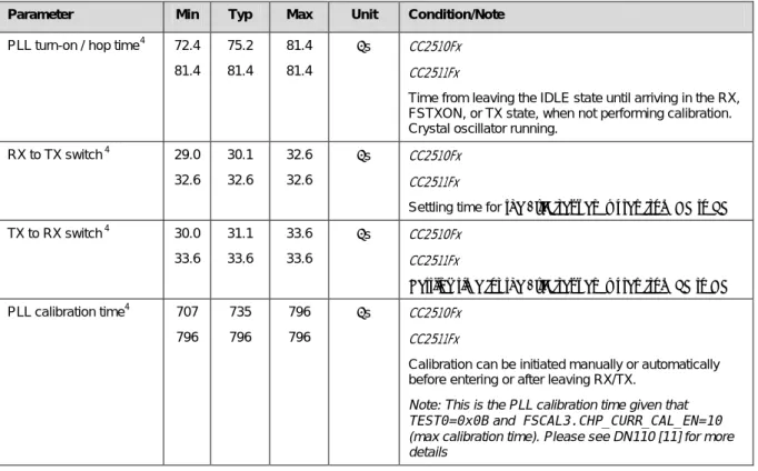
6.4 Crystal Oscillators
6.4.1 CC2510Fx Crystal Oscillator
TA = 25°C, VDD = 3.0 V if nothing else is stated.
Parameter Min Typ Max Unit Condition/Note
Crystal frequency 24 26 27 MHz Referred to as fXOSC. For operation below 26 MHz, please refer to Table
4 for Operating Conditions. Crystal frequency
accuracy requirement
±40 ppm This is the total tolerance including a) initial tolerance, b) crystal loading, c) aging, and d) temperature dependence.
The acceptable crystal tolerance depends on RF frequency and channel spacing / bandwidth.
C0 1 5 7 pF Simulated over operating conditions Load capacitance 10 13 20 pF Simulated over operating conditions ESR 100 Ω Simulated over operating conditions Start-up time 250 μs fXOSC= 26 MHz
Note: A Ripple counter of 12 bit is included to ensure duty-cycle requirements. Start-up time includes ripple counter delay until
SLEEP.XOSC_STB is asserted
Power Down Guard Time
3 ms The crystal oscillator must be in power down for a guard time before it is used again. This requirement is valid for all modes of operation. The need for power down guard time can vary with crystal type and load. Minimum figure is valid for reference crystal NDK, AT-41CD2 and load capacitance according to Table 29.
If power down guard time is violated, one of the consequences can be increased PER when using the radio immediately after the crystal oscillator has been reported stable.
Table 11: CC2510Fx Crystal Oscillator Parameters
6.4.2 CC2511Fx Crystal Oscillator
TA = 25°C, VDD = 3.0 V if nothing else is stated.
Parameter Min Typ Max Unit Condition/Note Crystal frequency 48 MHz Referred to as fXOSC
Crystal frequency accuracy requirement
±40 ppm This is the total tolerance including a) initial tolerance, b) crystal loading, c) aging, and d) temperature dependence.
The acceptable crystal tolerance depends on RF frequency and channel spacing / bandwidth.
C0
Fundamental 0.85 1 1.15 pF Simulated over operating conditions. Variation given by reference crystal NX2520SA from NDK
3rd overtone 2 3 7 pF
Load capacitance 15 16 17 pF Simulated over operating conditions ESR 60 Ω Simulated over operating conditions
Start-up time Note: A Ripple counter of 14 bit is included to ensure duty-cycle requirements. Start-up time includes ripple counter delay until
SLEEP.XOSC_STB is asserted
Fundamental 650 μs
3rd overtone 3 ms Simulated value
6.5 32.768 kHz Crystal Oscillator
TA = 25°C, VDD = 3.0V if nothing else is stated.
Parameter Min Typ Max Unit Condition/Note
Crystal frequency 32.768 kHz
C0 0.9 2.0 pF Simulated over operating conditions Load capacitance 12 16 pF Simulated over operating conditions ESR 40 130 kΩ Simulated over operating conditions
Start-up time 400 ms Value is simulated
Table 13: 32.768 kHz Crystal Oscillator Parameters 6.6 Low Power RC Oscillator
TA = 25°C, VDD = 3.0 V if nothing else is stated.
Parameter Min Typ Max Unit Condition/Note Calibrated frequency2 32.0 32.0 34.7 32.0 36.0 32.0 kHz CC2510Fx CC2511Fx
Calibrated low power RC oscillator frequency is
fRef / 750
Frequency accuracy after calibration
±1 %
Temperature coefficient +0.5 %/°C Frequency drift when temperature changes after calibration
Supply voltage coefficient +3 %/V Frequency drift when supply voltage changes after calibration
Initial calibration time 2 ms When the low power RC oscillator is enabled, calibration is continuously done in the background as long as the high speed crystal oscillator is running.
Table 14: Low Power RC Oscillator Parameters
6.7 High Speed RC Oscillator
TA = 25°C, VDD = 3.0 V if nothing else is stated.
Parameter Min Typ Max Unit Condition/Note
Calibrated frequency2 12 13 13.5 MHz Calibrated HS RCOSC frequency is fXOSC / 2
Uncalibrated frequency accuracy ±15 % Calibrated frequency accuracy ±1 % Start-up time 10 µs
Temperature coefficient −325 ppm/°C Frequency drift when temperature changes after calibration
Supply voltage coefficient
28 ppm/V Frequency drift when supply voltage changes after calibration
Calibration time 65 µs The HS RCOSC will be calibrated once when the high speed crystal oscillator is selected as system clock source (CLKCON.OSC is set to 0), and also when the system wakes up from PM{1 - 3} if CLKCON.OSC was set to 0 when entering PM{1 - 3}. See 12.1.5.1 for details).
Table 15: High Speed RC Oscillator Parameters 6.8 Frequency Synthesizer Characteristics
TA = 25°C, VDD = 3.0 V if nothing else stated. All measurement results are obtained using the CC2510EM reference designs ([1]).
Parameter Min Typ Max Unit Condition/Note Programmed frequency resolution3 366 366 397 366 412 366 Hz CC2510Fx CC2511Fx
Frequency resolution = fRef/ 216
Synthesizer frequency tolerance
±40 ppm Given by crystal used. Required accuracy (including temperature and aging) depends on frequency band and channel bandwidth / spacing.
RF carrier phase noise −77 dBc/Hz @ 50 kHz offset from carrier RF carrier phase noise −77 dBc/Hz @ 100 kHz offset from carrier RF carrier phase noise −78 dBc/Hz @ 200 kHz offset from carrier RF carrier phase noise −88 dBc/Hz @ 500 kHz offset from carrier RF carrier phase noise −98 dBc/Hz @ 1 MHz offset from carrier RF carrier phase noise −107 dBc/Hz @ 2 MHz offset from carrier RF carrier phase noise −116 dBc/Hz @ 5 MHz offset from carrier RF carrier phase noise −25 dBc/Hz @ 10 MHz offset from carrier
3
fRef = fXOSC for CC2510Fx and fRef = fXOSC /2 for CC2511Fx
For CC2510Fx Min figures are given using fXOSC = 24 MHz. Typ figures are given using fXOSC = 26 MHz,
Parameter Min Typ Max Unit Condition/Note PLL turn-on / hop time4 72.4
81.4 75.2 81.4 81.4 81.4 µs CC2510Fx CC2511Fx
Time from leaving the IDLE state until arriving in the RX, FSTXON, or TX state, when not performing calibration. Crystal oscillator running.
RX to TX switch 4 29.0 32.6 30.1 32.6 32.6 32.6 µs CC2510Fx CC2511Fx
Settling time for the 1∙IF frequency step from RX to TX TX to RX switch 4 30.0 33.6 31.1 33.6 33.6 33.6 µs CC2510Fx CC2511Fx
Settling time for the 1∙IF frequency step from TX to RX PLL calibration time4 707 796 735 796 796 796 µs CC2510Fx CC2511Fx
Calibration can be initiated manually or automatically before entering or after leaving RX/TX.
Note: This is the PLL calibration time given that
TEST0=0x0B and FSCAL3.CHP_CURR_CAL_EN=10
(max calibration time). Please see DN110 [11] for more details
Table 16: Frequency Synthesizer Parameters 6.9 Analog Temperature Sensor
TA= 25°C, VDD = 3.0V if nothing else stated. All measurement results are obtained using the CC2510EM reference designs ([1]).
Parameter Min Typ Max Unit Condition/Note Output voltage at −40°C 0.654 V
Output voltage at 0°C 0.750 V Output voltage at 40°C 0.848 V Output voltage at 80°C 0.946 V
Temperature coefficient 2.43 mV/°C Fitted from −20°C to 80°C Error in calculated
temperature, calibrated
−2 *
0 2 * °C From −20°C to 80°C when using 2.43 mV/°C, after 1-point calibration at room temperature
*
The indicated minimum and maximum error with 1-point calibration is based on measured values for typical process parameters
Current consumption increase when enabled
0.3 mA
6.10 7 - 12 bit ADC
TA = 25°C, VDD = 3.0V if nothing else stated. The numbers given here are based on tests performed in accordance with IEEE Std 1241-2000 [7]. The ADC data are from CC2430 characterization. As the
CC2510x/C2511Fx uses the same ADC, the numbers listed in Table 18 should be good indicators of the performance to be expected from CC2510x and CC2511x. Note that these numbers will apply for 24 MHz operated systems (like CC2510x using a 24 MHz crystal or CC2511x using a 48 MHz crystal). Performance will be slightly different for other crystal frequencies (e.g. 26 MHz and 27 MHz).
Parameter Min Typ Max Unit Condition/Note
Input voltage 0 VDD V VDD is the voltage on the AVDD pin (2.0 - 3.6 V) External reference
voltage
0 VDD V VDD is the voltage on the AVDD pin (2.0 - 3.6 V) External reference
voltage differential
0 VDD V VDD is the voltage on the AVDD pin (2.0 - 3.6 V)
Input resistance, signal 197 kΩ Simulated using 4 MHz clock speed (see Section 12.10.2.7) Full-Scale Signal5 2.97 V Peak-to-peak, defines 0 dBFS
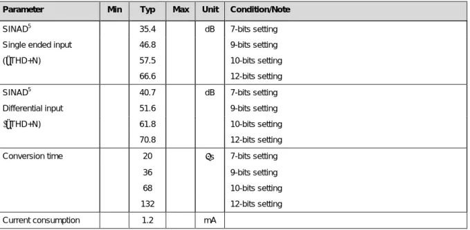
ENOB5 5.7 bits 7-bits setting Single ended input 7.5 9-bits setting
9.3 10-bits setting 10.8 12-bits setting
ENOB5 6.5 bits 7-bits setting
Differential input 8.3 9-bits setting 10.0 10-bits setting 11.5 12-bits setting
Useful Power Bandwidth 0 - 20 kHz 7-bits setting, both single and differential THD5
-Single ended input −75.2 dB 12-bits setting, −6 dBFS -Differential input −86.6 12-bits setting, −6 dBFS Signal To Non-Harmonic
Ratio5
-Single ended input 70.2 dB 12-bits setting -Differential input 79.3 12-bits setting Spurious Free Dynamic
Range5
-Single ended input 78.8 dB 12-bits setting, −6 dBFS -Differential input 88.9 12-bits setting, −6 dBFS
CMRR, differential input <−84 dB 12- bit setting, 1 kHz Sine (0 dBFS), limited by ADC resolution Crosstalk, single ended
input
<−84 dB 12- bit setting, 1 kHz Sine (0 dBFS), limited by ADC resolution
Offset −3 mV Mid. Scale
Gain error 0.68 %
DNL5 0.05 LSB 12-bits setting, mean 0.9 12-bits setting, max
INL5 4.6 LSB 12-bits setting, mean
13.3 12-bits setting, max
5
Parameter Min Typ Max Unit Condition/Note
SINAD5 35.4 dB 7-bits setting
Single ended input 46.8 9-bits setting
(−THD+N) 57.5 10-bits setting
66.6 12-bits setting
SINAD5 40.7 dB 7-bits setting
Differential input 51.6 9-bits setting
(−THD+N) 61.8 10-bits setting
70.8 12-bits setting Conversion time 20 µs 7-bits setting
36 9-bits setting 68 10-bits setting 132 12-bits setting Current consumption 1.2 mA
6.11 Control AC Characteristics
TA = 25°C, VDD = 3.0 V if nothing else stated. All measurement results are obtained using the CC2510EM reference designs ([1]).
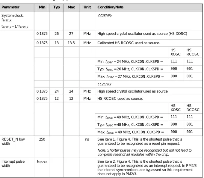
Parameter Min Typ Max Unit Condition/Note System clock,
fSYSCLK
tSYSCLK= 1/ fSYSCLK
CC2510Fx
0.1875 26 27 MHz High speed crystal oscillator used as source (HS XOSC) 0.1875 13 13.5 MHz Calibrated HS RCOSC used as source.
HS XOSC
HS RCOSC Min: fXOSC = 24 MHz, CLKCON.CLKSPD = 111 111
Typ: fXOSC = 26 MHz, CLKCON.CLKSPD = 000 001
Max: fXOSC = 27 MHz, CLKCON.CLKSPD = 000 001
CC2511Fx
0.1875 24 24 MHz High speed crystal oscillator used as source. 0.1875 12 12 MHz HS RCOSC used as source.
HS XOSC
HS RCOSC Min: fXOSC = 48 MHz, CLKCON.CLKSPD = 111 111
Typ: fXOSC = 48 MHz, CLKCON.CLKSPD = 000 001
Max: fXOSC = 48 MHz, CLKCON.CLKSPD = 000 001
RESET_N low width
250 ns See item 1, Figure 4. This is the shortest pulse that is guaranteed to be recognized as a reset pin request.
Note: Shorter pulses may be recognized but will not lead to complete reset of all modules within the chip.
Interrupt pulse width
tSYSCLK See item 2, Figure 4. This is the shortest pulse that is guaranteed to be recognized as an interrupt request. In PM2/3 the internal synchronizers are bypassed so this requirement does not apply in PM2/3.
Table 19: Control Inputs AC Characteristics
1 2 2 RESET_N Px_n Px_n
6.11.1 Filtering of RESET_N pin
The RESET_N pin is sensitive to noise and can cause unintended reset of the chip. For a long reset line add an external RC filter with values 1 nF and 2.7 kΩ close to the RESET_N pin. When doing this, note that the RESET_N low width (the shortest pulse that is guaranteed to be recognized as a reset pin request) is longer than stated in Table 19.
6.12 SPI AC Characteristics
TA = 25°C, VDD = 3.0V if nothing else stated. All measurement results are obtained using the CC2510EM reference designs ([1]).
Parameter Min Typ Max Unit Condition/Note
SCK period See Section 12.14.3 ns Master. See item 1, Figure 5
SCK duty cycle 50 % Master.
SSN low to SCK 2∙tSYSCLK See item 5, Figure 5 SCK to SSN high 30 ns See item 6, Figure 5
MISO setup 10 ns Master. See item 2, Figure 5
MISO hold 10 ns Master. See item 3, Figure 5
SCK to MOSI 25 ns Master. See item 4, Figure 5, load = 10 pF SCK period 100 ns Slave. See item 1, Figure 5
SCK duty cycle 50 % Slave.
MOSI setup 10 ns Slave. See item 2, Figure 5
MOSI hold 10 ns Slave. See item 3, Figure 5
SCK to MISO 25 ns Slave. See item 4, Figure 5, load = 10 pF
Table 20: SPI AC Characteristics
1 3 2 SCK MISO/MOSI MOSI/MISO 4 SSN 5 6
6.13 Debug Interface AC Characteristics
TA = 25°C, VDD = 3.0 V if nothing else stated. All measurement results are obtained using the CC2510EM reference designs ([1]).
Parameter Min Typ Max Unit Condition/Note Debug clock period 125 ns See item 1, Figure 6
Note: CLKCON.CLKSPD must be 000 or 001 when using the debug interface
Debug data setup 5 ns See item 2, Figure 6 Debug data hold 5 ns See item 3, Figure 6
Clock to data delay 10 ns See item 4, Figure 6, load = 10 pF RESET_N inactive
after P2_2 rising
10 ns See item 5, Figure 6
Table 21: Debug Interface AC Characteristics
1 3 2 DEBUG CLK P2_2 DEBUG DATA P2_1 DEBUG DATA P2_1 4 5 RESET_N
Figure 6: Debug Interface AC Characteristics 6.14 Port Outputs AC Characteristics
TA = 25°C, VDD = 3.0 V if nothing else stated. All measurement results are obtained using the CC2510EM reference designs ([1]).
Parameter Min Typ Max Unit Condition/Note P0_[0:7], P1_[2:7], P2_[0:4] Port output rise time (IOCFG1.GDO_DS=0 / IOCFG1.GDO_DS=1) 3.15 / 1.34 ns Load = 10 pF
Timing is with respect to 10% VDD and 90% VDD levels. Values are estimated
P0_[0:7], P1_[2:7], P2_[0:4] Port output fall time (IOCFG1.GDO_DS=0 / IOCFG1.GDO_DS=1) 3.2 / 1.44 ns Load = 10 pF
Timing is with respect to 90% VDD and 10% VDD. Values are estimated
6.15 Timer Inputs AC Characteristics
TA = 25°C, VDD = 3.0 V if nothing else stated. All measurement results are obtained using the CC2510EM reference designs ([1]).
Parameter Min Typ Max Unit Condition/Note
Input capture pulse width tSYSCLK Synchronizers determine the shortest input pulse that can be recognized. The synchronizers operate from the current system clock rate (see Table 19)
Table 23: Timer Inputs AC Characteristics 6.16 DC Characteristics
The DC Characteristics of CC2510Fx/CC2511Fx are listed in Table 24 below.
TA = 25°C, VDD = 3.0 V if nothing else stated. All measurement results are obtained using the CC2510EM reference designs ([1]).
Digital Inputs/Outputs Min Typ Max Unit Condition
Logic "0" input voltage 30 % Of VDD supply (2.0 - 3.6 V) Logic "1" input voltage 70 % Of VDD supply (2.0 - 3.6 V) Logic "0" input current per pin NA 12 nA Input equals 0 V
Logic "1" input current per pin NA 12 nA Input equals VDD Total logic “0” input current all pins 70 nA
Total logic “1” input current all pins 70 nA I/O pin pull-up and pull-down resistor 20 kΩ
7
Pin and I/O Port Configuration
The CC2510Fx pin-out is shown in Figure 7 and Table 25. See Section 12.4 for details on the I/O configuration. AGND Exposed die attached pad RESET_N DVDD P1_6 36 35 34 33 32 31 30 29 28 9 8 7 6 5 4 3 2 1 27 26 25 24 23 22 21 20 19 10 11 12 13 14 15 16 17 18 P1_1 P1_0 P0_0 P0_1 P0_2 P0_3 P0_4 DVDD P0_5 P0_6 P0_7 P2_0 P2_1 P2_2 P2_3/XSOC32_Q1 P2_4/XOSC32_Q2 AVDD XOSC_Q2 AVDD RF_N AVDD AVDD RBIAS XOSC_Q1 RF_P P1_3 P1_4 P1_5 P1_7 AVDD_DREG GUARD P1_2 DCOUPL
Figure 7: CC2510Fx Pinout Top View
Note: The exposed die attach pad must be connected to a solid ground plane as this is the ground connection for the chip.
Pin Pin Name Pin Type Description
- AGND Ground The exposed die attach pad must be connected to a solid ground plane
1 P1_2 D I/O Port 1.2
2 DVDD Power (Digital) 2.0 V - 3.6 V digital power supply for digital I/O
3 P1_1 D I/O Port 1.1 4 P1_0 D I/O Port 1.0 5 P0_0 D I/O Port 0.0 6 P0_1 D I/O Port 0.1 7 P0_2 D I/O Port 0.2 8 P0_3 D I/O Port 0.3 9 P0_4 D I/O Port 0.4
10 DVDD Power (Digital) 2.0 V - 3.6 V digital power supply for digital I/O
11 P0_5 D I/O Port 0.5 12 P0_6 D I/O Port 0.6 13 P0_7 D I/O Port 0.7 14 P2_0 D I/O Port 2.0 15 P2_1 D I/O Port 2.1 16 P2_2 D I/O Port 2.2
17 P2_3/XOSC32_Q1 D I/O Port 2.3/32.768 kHz crystal oscillator pin 1 18 P2_4/XOSC32_Q2 D I/O Port 2.4/32.768 kHz crystal oscillator pin 2 19 AVDD Power (Analog) 2.0 V - 3.6 V analog power supply connection 20 XOSC_Q2 Analog I/O Crystal oscillator pin 2
21 XOSC_Q1 Analog I/O Crystal oscillator pin 1, or external clock input 22 AVDD Power (Analog) 2.0 V - 3.6 V analog power supply connection 23 RF_P RF I/O Positive RF input signal to LNA in receive mode
Positive RF output signal from PA in transmit mode 24 RF_N RF I/O Negative RF input signal to LNA in receive mode
Negative RF output signal from PA in transmit mode 25 AVDD Power (Analog) 2.0 V - 3.6 V analog power supply connection 26 AVDD Power (Analog) 2.0 V - 3.6 V analog power supply connection 27 RBIAS Analog I/O External precision bias resistor for reference current 28 GUARD Power (Digital) Power supply connection for digital noise isolation
29 AVDD_DREG Power (Digital) 2.0 V - 3.6 V digital power supply for digital core voltage regulator 30 DCOUPL Power
decoupling
1.8 V digital power supply decoupling 31 RESET_N DI Reset, active low
32 P1_7 D I/O Port 1.7
33 P1_6 D I/O Port 1.6
34 P1_5 D I/O Port 1.5
35 P1_4 D I/O Port 1.4
36 P1_3 D I/O Port 1.3
The CC2511Fx pin-out is shown in Figure 8 and Table 26. See Section 12.4 for details on the I/O configuration. AGND Exposed die attached pad RESET_N DVDD P1_6 36 35 34 33 32 31 30 29 28 9 8 7 6 5 4 3 2 1 27 26 25 24 23 22 21 20 19 10 11 12 13 14 15 16 17 18 P1_1 P1_0 P0_0 P0_1 P0_2 P0_3 P0_4 DP DM DVDD P0_5 P2_0 P2_1 P2_2 P2_3/XSOC32_Q1 P2_4/XOSC32_Q2 AVDD XOSC_Q2 AVDD RF_N AVDD AVDD R_BIAS XOSC_Q1 RF_P P1_3 P1_4 P1_5 P1_7 AVDD_DREG GUARD P1_2 DCOUPL
Figure 8: CC2511Fx Pin-out Top View
Note: The exposed die attach pad must be connected to a solid ground plane as this is the ground connection for the chip.
Pin Pin Name Pin Type Description
- AGND Ground The exposed die attach pad must be connected to a solid ground plane
1 P1_2 D I/O Port 1.2
2 DVDD Power (Digital) 2.0 V - 3.6 V digital power supply for digital I/O
3 P1_1 D I/O Port 1.1 4 P1_0 D I/O Port 1.0 5 P0_0 D I/O Port 0.0 6 P0_1 D I/O Port 0.1 7 P0_2 D I/O Port 0.2 8 P0_3 D I/O Port 0.3 9 P0_4 D I/O Port 0.4
10 DP USB I/O USB Differential Data Bus Plus 11 DM USB I/O USB Differential Data Bus Minus
12 DVDD Power (Digital) 2.0 V - 3.6 V digital power supply for digital I/O 13 P0_5 D I/O Port 0.5
14 P2_0 D I/O Port 2.0 15 P2_1 D I/O Port 2.1 16 P2_2 D I/O Port 2.2
17 P2_3/XOSC32_Q1 D I/O Port 2.3/32.768 kHz crystal oscillator pin 1 18 P2_4/XOSC32_Q2 D I/O Port 2.4/32.768 kHz crystal oscillator pin 2 19 AVDD Power (Analog) 2.0 V - 3.6 V analog power supply connection 20 XOSC_Q2 Analog I/O Crystal oscillator pin 2
21 XOSC_Q1 Analog I/O Crystal oscillator pin 1, or external clock input 22 AVDD Power (Analog) 2.0 V - 3.6 V analog power supply connection 23 RF_P RF I/O Positive RF input signal to LNA in receive mode
Positive RF output signal from PA in transmit mode 24 RF_N RF I/O Negative RF input signal to LNA in receive mode
Negative RF output signal from PA in transmit mode 25 AVDD Power (Analog) 2.0 V - 3.6 V analog power supply connection 26 AVDD Power (Analog) 2.0 V - 3.6 V analog power supply connection 27 RBIAS Analog I/O External precision bias resistor for reference current 28 GUARD Power (Digital) Power supply connection for digital noise isolation
29 AVDD_DREG Power (Digital) 2.0 V - 3.6 V digital power supply for digital core voltage regulator 30 DCOUPL Power
decoupling
1.8 V digital power supply decoupling 31 RESET_N DI Reset, active low
32 P1_7 D I/O Port 1.7 33 P1_6 D I/O Port 1.6 34 P1_5 D I/O Port 1.5 35 P1_4 D I/O Port 1.4 36 P1_3 D I/O Port 1.3
8
Circuit Description
Figure 9: C C2510Fx/CC2511Fx Block Diagram
A block diagram of CC2510Fx/CC2511Fx is shown in Figure 9. The modules can be divided into one out of three categories: CPU-related modules, radio-related modules, and modules
related to power, test, and clock distribution. In the following subsections, a short description of each module that appears in Figure 9.
8.1 CPU and Peripherals
The 8051 CPU core is a single-cycle 8051-compatible core. It has three different memory access buses (SFR, DATA and CODE/XDATA), a debug interface, and an extended interrupt unit servicing 18 interrupt sources. See Section 10 for details on the CPU.
The memory crossbar/arbitrator is at the heart of the system as it connects the CPU and DMA controller with the physical memories and all peripherals through the SFR bus. The memory arbitrator has four memory access points, access at which can map to one of three physical memories on the
CC2510Fx and one of four physical memories
on the CC2511Fx: a 1/2/4 KB SRAM, 8/16/32 KB flash memory, RF/I2S registers, and USB registers (CC2511Fx). The memory arbitrator is responsible for performing arbitration and sequencing between simultaneous memory accesses to the same physical memory. The SFR bus is drawn conceptually in the block diagram as a common bus that connects
all hardware peripherals, except USB, to the memory arbitrator. The SFR bus also provides access to the radio registers and I2S registers in the radio register bank even though these are indeed mapped into XDATA memory space.
The 1/2/4 KB SRAM maps to the DATA memory space and part of the XDATA and CODE memory spaces. The memory is an ultra-low-power SRAM that retains its contents even when the digital part is powered off (PM2 and PM3).
The 8/16/32 KB flash block provides in-circuit programmable non-volatile program memory for the device and maps into the CODE and XDATA memory spaces. Table 27 shows the available devices in the CC2510/CC2511 family. The available devices differ only in flash memory size. Writing to the flash block is performed through a Flash Controller that allows page-wise (1024 byte) erasure and 2-byte-wise reprogramming. See Section 12.3 for details. Device Flash [KB] CC2510F8 8 CC2511F8 8 CC2510F16 16 CC2511F16 16 CC2510F32 32 CC2511F32 32
Table 27: CC2510/CC2511 Flash Memory Options
A versatile five-channel DMA controller is available in the system. It accesses memory using a unified memory space and has therefore access to all physical memories. Each channel is configured (trigger event, priority, transfer mode, addressing mode, source and destination pointers, and transfer count) with DMA descriptors anywhere in memory. Many of the hardware peripherals rely on the DMA controller for efficient operation (AES core, Flash Controller, USARTs, Timers, and ADC interface) by performing data transfers between a single SFR address and flash/SRAM. See Section 12.5 for details.
serviced even if the device is in PM1, PM2, or PM3 by bringing the CC2510Fx/CC2511Fx back to active mode.
The debug interface implements a proprietary two-wire serial interface that is used for in-circuit debugging. Through this debug interface it is possible to perform an erasure of the entire flash memory, control which oscillators are enabled, stop and start execution of the user program, execute supplied instructions on the 8051 core, set code breakpoints, and single step through instructions in the code. Using these techniques it is possible to perform in-circuit
certain pins or if they are under software control. In the latter case, each pin can be configured as an input or output and it is also possible to configure the input mode to be pull-up, pull-down, or tristate. Each peripheral that connects to the I/O-pins can choose between two different I/O pin locations to ensure flexibility in various applications. See Section 12.4 for details.
The Sleep Timer is an ultra-low power timer which uses a 32.768 kHz crystal oscillator or a low power RC oscillator as clock source. The Sleep Timer runs continuously in all operating modes except active mode and PM3 and is typically used to get out of PM0, PM1, or PM2. See Section 12.8 for details.
A built-in watchdog timer allows the
CC2510Fx/CC2511Fx to reset itself in case the firmware hangs. When enabled, the watchdog timer must be cleared periodically, otherwise it will reset the device when it times out. See Section 12.13 for details.
Timer 1 is a 16-bit timer which supports typical timer/counter functions such as input capture, output compare, and PWM functions. The timer has a programmable prescaler, a 16-bit period value, and three independent capture/compare channels. Each of the channels can be used as PWM outputs or to capture the timing of edges on input signals. A second order Delta-Sigma noise shaper mode is also supported for audio applications. See Section 12.6 for details.
Timer 2 (MAC timer) is specially designed to support time-slotted protocols in software. The timer has a configurable timer period and a programmable prescaler range. See Section 12.7 for details.
Timers 3 and Timer 4 are two 8-bit timers which supports typical timer/counter functions such as output compare and PWM functions. They have a programmable prescaler, an 8-bit period value, and two compare channels each, which can be used as PWM outputs. See Section 12.9 for details.
USART 0 and USART 1 are each configurable as either an SPI master/slave or a UART. They provide hardware flow-control and double buffering on both RX and TX and are thus well suited for high-throughput, full-duplex applications. Each has its own high-precision baud-rate generator, hence leaving the ordinary timers free for other uses. When configured as an SPI slave they sample the
input signal using SCK directly instead of using some over-sampling scheme and are therefore well-suited for high data rates. See Section 12.14 for details.
The AES encryption/decryption core allows the user to encrypt and decrypt data using the AES algorithm with 128-bit keys. See Section 12.12 for details.
The ADC supports 7 to 12 bits of resolution in a 30 kHz to 4 kHz bandwidth respectively. DC and audio conversions with up to eight input channels (P0) are possible (CC2511Fx is limited to six channels). The inputs can be selected as single ended or differential. The reference voltage can be internal, VDD, or a single ended or differential external signal. The ADC also has a temperature sensor input channel. The ADC can automate the process of periodic sampling or conversion over a sequence of channels. See Section 12.10 for details.
The USB allows the CC2511Fx to implement a Full-Speed USB 2.0 compatible device. The USB has a dedicated 1 KB SRAM that is used for the endpoint FIFOs. 5 endpoints are available in addition to control endpoint 0. Each of these endpoints must be configured as Bulk/Interrupt or Isochronous and can be used as IN, OUT or IN/OUT. Double buffering of packets is also supported for endpoints 1 - 5. The maximum FIFO memory available for each endpoint is as follows: 32 bytes for endpoint 0, 32 bytes for endpoint 1, 64 bytes for endpoint 2, 128 bytes for endpoint 3, 256 bytes for endpoint 4, and 512 bytes for endpoint 5. When an endpoint is used as IN/OUT, the FIFO memory available for the endpoint can be distributed between IN and OUT depending on the demands of the application. The USB does not exist on the
CC2510Fx. See Section 12.16 for details.
The I2S can be used to send/receive audio samples to/from an external sound processor or DAC and may operate at full or half duplex. Samples of up to 16-bits resolution can be used although the I2S can be configured to send more low order bits if necessary to be compliant with the resolution of the receiver (up to 32 bit). The maximum bit-rate supported is 3.5 Mbps. The I2S can be configured as a master or slave device and supports both mono and stereo. Automatic µ-Law expansion and compression can also be configured. See Section 12.15 for details.
8.2 Radio
CC2510Fx/CC2511Fx features an RF transceiver based on the industry-leading CC2500,
requiring very few external components. See Section 13 for details.
9
Application Circuit
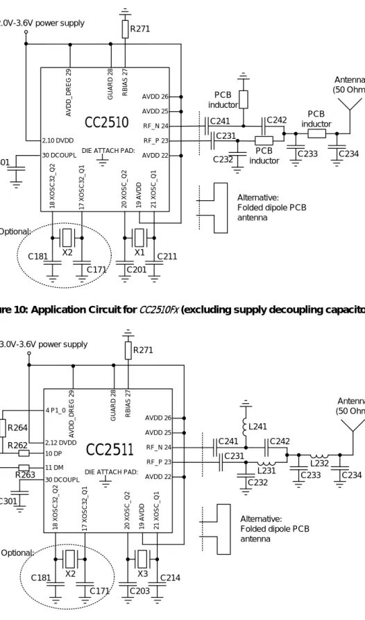
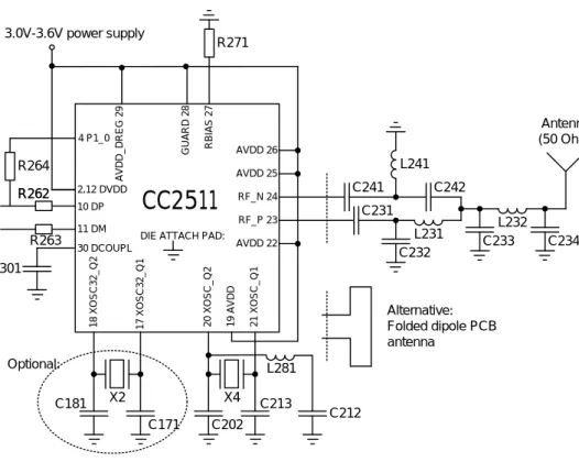
Only a few external components are required for using the CC2510Fx/CC2511Fx. The recommended application circuit for CC2510Fx is shown in Figure 10. The recommended application circuits for CC2511Fx are shown in Figure 11 and Figure 12. The first of the
recommended CC2511Fx circuit uses a fundamental crystal and the second uses a 3rd overtone crystal. The external components are described in Table 28, and typical values are given in Table 29.
9.1 Bias Resistor
The bias resistor R271 is used to set an accurate bias current.
9.2 Balun and RF Matching
The balanced RF input and output of
CC2510Fx/CC2511Fx share two common pins and
are designed for a simple, low-cost matching and balun network on the printed circuit board. The RX- and TX switching at the
CC2510Fx/CC2511Fx front-end are controlled by a dedicated on-chip function, eliminating the need for an external RX/TX-switch.
A few passive external components combined with the internal RX/TX switch/termination circuitry ensures match in both RX and TX mode.
Although CC2510Fx/CC2511Fx has a balanced RF input/output, the chip can be connected to a single-ended antenna with few external low cost capacitors and inductors.
The passive matching/filtering network connected to CC2510Fx/CC2511Fx should have the following differential impedance as seen from the RF-port (RF_P and RF_N) towards the antenna:
Zout = 80 + j74 Ω
C232, C242, and two inductive transmission PCB lines form the recommended balun that converts the differential RF port on CC2510Fx to a single-ended RF signal. For the CC2511Fx balun, the inductive PCB lines are replaced by L241 and L231. Note that either of the solutions (PCB lines or discrete components) can be used for both the chips. C241 and C231 are needed for DC blocking. Together with an appropriate LC filter network, the balun components also transform the impedance to match a 50 Ω antenna (or cable). Component values for the RF balun and LC network are found in the latest CC2510EM and CC2511Dongle reference designs ([1] and [2]). Suggested values are also listed in Table 29. The balun and LC filter component values, their placement and layout are important in order to keep the performance of the
CC2510Fx/CC2511Fx optimized. It is highly
recommended to follow the CC2510EM / CC2511Dongle reference designs. Gerber files and schematics for the reference designs are available for download from the TI website
9.3 Crystal
The crystal oscillator for the CC2510Fx uses an external crystal X1, with two loading capacitors (C201 and C211) (see Figure 10 and Table 28).
The CC2511Fx should use a 48 MHz
(L281) must also be connected in series with C212 (see Figure 11, Figure 12 and Table 28).
Note: The high speed crystal oscillator must be stable (SLEEP.XOSC_STB=1)
and loading capacitors C181 and C171. This crystal can be used by the Sleep Timer if more accurate wake-up intervals are needed than what the internal RC oscillator can provide. When not using X2, P2_3 and P2_4 may be used as general IO pins.
The loading capacitor values depend on the total load capacitance, CL, specified for the crystal. The total load capacitance seen between the crystal terminals should equal CL for the crystal to oscillate at the specified frequency. For the CC2510Fx using the crystal X1, the load capacitance CL is given as:
Parasitic L C C C C + + = 201 211 1 1 1
The parasitic capacitance is constituted by pin input capacitance and PCB stray capacitance. Total parasitic capacitance is typically 2.5 pF. The crystal oscillator is amplitude regulated. This means that a high current is used to start up the oscillations. When the amplitude builds up, the current is reduced to what is necessary to maintain approximately 0.4 Vpp signal swing. This ensures a fast start-up, and keeps the drive level to a minimum. The ESR of the crystal should be within the specification in order to ensure a reliable start-up
9.4 Reference Signal
The chip can alternatively be operated with a reference signal from 24 to 27 MHz (CC2510Fx) or 48 MHz (CC2511Fx) instead of a crystal. This input clock can either be a full-swing digital signal (0 V to VDD) or a sine wave of maximum 1 V peak-peak amplitude. The reference signal must be connected to the XOSC_Q1 input. The sine wave must be
connected to XOSC_Q1 using a serial capacitor. When using a full-swing digital signal this capacitor can be omitted. The XOSC_Q2 line must be left un-connected. The crystal loading capacitors and crystal inductor (if using X4) can be omitted when using a reference signal.
9.5 USB (CC2511Fx)
For the CC2511Fx, the DP and DM pins need series resistors R262 and R263 for impedance matching and the D+ line must have a pull-up resistor, R264. The series resistors should match the 90 Ω ±15% characteristic impedance of the USB bus.
Notice that the pull-up resistor must be tied to a voltage source between 3.0 and 3.6 V (typically 3.3 V). The voltage source must be
derived from or controlled by the VBUS power supply provided by the USB cable. In this way, the pull-up resistor does not provide current to the D+ line when VBUS is removed. The pull-up resistor may be connected directly between VBUS and the D+ line. As an alternative, if the
CC2511Fx firmware needs the ability to
disconnect from the USB bus, an I/O pin on the CC2511Fx can be used to control the pull-up resistor.
9.6 Power Supply Decoupling
The power supply must be properly decoupled close to the supply pins. Note that decoupling capacitors are not shown in the application circuit. The placement and the size of the
decoupling capacitors are very important to achieve the optimum performance. TI provides reference designs that should be followed closely ([1] and [2]).
C171
Antenna (50 Ohm) 2.0V-3.6V power supply
20 XOSC_Q2 19 AVDD 21 XOSC_Q1
AVDD_DREG 29 GUARD 28 RBIAS 27 2,10 DVDD 30 DCOUPL AVDD 26 AVDD 25 RF_N 24 RF_P 23 AVDD 22 X1 C242 inductorPCB C233 C234 R271 C201 C211 C301
CC2510
DIE ATTACH PAD:C241 C231 Alternative: Folded dipole PCB antenna X2 C181 18 XOSC32_Q2 17 XOSC32_Q1 Optional: PCB inductor PCB inductor C232
Figure 10: Application Circuit for CC2510Fx (excluding supply decoupling capacitors)
D+ D-C171 Antenna (50 Ohm) 3.0V-3.6V power supply
20 XOSC_Q2 19 AVDD 21 XOSC_Q1
AVDD_DREG 29 GUARD 28 RBIAS 27 2,12 DVDD 30 DCOUPL AVDD 26 AVDD 25 RF_N 24 RF_P 23 AVDD 22 X3 C232 C242 L241 L231 L232 C233 C234 R271 C203 C214 C301
CC2511
DIE ATTACH PAD:C241 C231 Alternative: Folded dipole PCB antenna X2 C181 18 XOSC32_Q2 17 XOSC32_Q1 Optional: R262 R263 R264 10 DP 11 DM 4 P1_0
Figure 11: Application Circuit for CC2511Fx with Fundamental Crystal (excluding supply decoupling capacitors)
D+ D-C171 Antenna (50 Ohm) 3.0V-3.6V power supply
20 XOSC_Q2 19 AVDD 21 XOSC_Q1
AVDD_DREG 29 GUARD 28 RBIAS 27 2,12 DVDD 30 DCOUPL AVDD 26 AVDD 25 RF_N 24 RF_P 23 AVDD 22 X4 C232 C242 L241 L231 C233L232 C234 R271 C202 C213 C301
CC2511
DIE ATTACH PAD:C241 C231 Alternative: Folded dipole PCB antenna X2 C181 18 XOSC32_Q2 17 XOSC32_Q1 Optional: R262 R263 10 DP 11 DM C212 L281 R262 R264 4 P1_0
Figure 12: Application Circuit for CC2511Fx with 3rd Overtone Crystal (excluding supply decoupling capacitors)
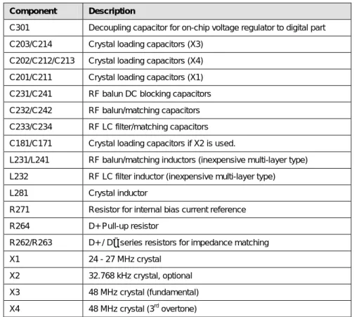
Component Description
C301 Decoupling capacitor for on-chip voltage regulator to digital part C203/C214 Crystal loading capacitors (X3)
C202/C212/C213 Crystal loading capacitors (X4) C201/C211 Crystal loading capacitors (X1) C231/C241 RF balun DC blocking capacitors C232/C242 RF balun/matching capacitors C233/C234 RF LC filter/matching capacitors C181/C171 Crystal loading capacitors if X2 is used.
L231/L241 RF balun/matching inductors (inexpensive multi-layer type) L232 RF LC filter inductor (inexpensive multi-layer type) L281 Crystal inductor
R271 Resistor for internal bias current reference R264 D+ Pull-up resistor
R262/R263 D+ / D− series resistors for impedance matching X1 24 - 27 MHz crystal
X2 32.768 kHz crystal, optional X3 48 MHz crystal (fundamental) X4 48 MHz crystal (3rd overtone)