with GaAs quantum wells
A. A. Demenev,1V. D. Kulakovskii,1 C. Schneider,2S. Brodbeck,2M. Kamp,2S. H¨ofling,2, 3 S. V. Lobanov,4T. Weiss,5N. A. Gippius,6, 7 and S. G. Tikhodeev7, 1, 8,a)
1)Institute of Solid State Physics, Russian Academy of Science, Chernogolovka 142432, Russia
2)
Technische Physik and Wilhelm-Conrad-R¨ontgen-Research Center for Complex Material Systems, Universit¨at W¨urzburg, D-97074 W¨urzburg, Am Hubland, Germany
3)
SUPA, School of Physics and Astronomy, University of St Andrews, St Andrews, KY16 9SS, United Kingdom
4)School of Physics and Astronomy, Cardiff University, Cardiff CF24 3AA, United Kingdom 5)
4th Physics Institute and Research Center SCoPE, University of Stuttgart, Stuttgart D-70550, Germany
6)Skolkovo Institute of Science and Technology, Novaya Street 100, Skolkovo 143025, Russia
7)
A. M. Prokhorov General Physics Institute, Russian Academy of Sciences, Vavilova Street 38, Moscow 119991, Russia
8)M. V. Lomonosov Moscow State University, Leninskie Gory 1, Moscow 119991, Russia
(Dated: 11 October 2016)
We report the elliptically, close to circularly polarized lasing at~ω= 1.473 and 1.522 eV from an AlAs/AlGaAs Bragg microcavity with 12 GaAs quantum wells in the active region and chiral-etched upper distributed Bragg refractor under optical pump at room temperature. The advantage of using the chiral photonic crystal with a large contrast of dielectric permittivities is its giant optical activity, allowing to fabricate a very thin half-wave plate, with a thickness of the order of the emitted light wavelength, and to realize the monolithic control of circular polarization.
PACS numbers: 71.36.+c, 42.65.Pc, 42.55.Sa
Modern nanofabrication technologies allow to realize photonic structures — photonic crystals and metamate-rials — with extraordinary optical properties1–3. In
par-ticular, chiral photonic structures are known to demon-strate a giant optical activity, several orders of magnitude stronger than natural materials4–9. Recently, it has been
demonstrated that incorporating a chiral photonic struc-ture into a planar GaAs waveguide or a semiconductor microcavity (MC) with embedded light-emitting achiral InAs quantum dots (QD) allows to achieve light emis-sion with a high degree of circular polarization (DCP), without applying magnetic field and without the need of thick quarter-waveplates10–12. The effect is due to the modification of the symmetry and density of environmen-tally allowed electromagnetic modes relative to that in free space due to the chiral nanostructuring, which, in turn, affects the spontaneous emission rate, directional pattern, and polarization13,14. This method has consid-erable advantages: small size, very simple operation, and compatibility with semiconductor fabrication process. In this Letter we demonstrate that the method works for the stimulated emission as well, and demonstrate a highly circularly polarized lasing from an AlGaAs/AlAs micro-cavity with chirally etched top Bragg mirror with GaAs quantum wells (QW) in the active cavity. Previously, the
elliptically polarized lasing with a good DCP was real-ized on a quantum cascade laser with monolithic control of circular polarization in the THz range of frequencies15.
A chiral photonic crystal (CPC), a monolithic part of the upper cavity mirror, is fabricated from the AlAs/AlGaAs/GaAs high Q-factor MC grown by molec-ular beam epitaxy on a (001)-oriented GaAs. The full planar cavity consists of a lower and an upper Bragg re-flectors with 27 and 23 pairs of AlAs/Al0.20Ga0.80As
lay-ers, respectively, with 3 nm GaAs smoothing layer after each pair in the Bragg reflectors and an active layer with three groups of four 13 nm GaAs QWs separated by 4 nm AlAs bariers. The nominal thicknesses of the AlAs and Al0.20Ga0.80As layers in Bragg mirrors are (68 ±3) nm
and (58±3) nm, respectively. The Bragg pairs are de-posited on the wafer with a slight wedge from the center to the circumference, resulting in a blueshift of the cavity resonance which can amount up to ≈200 meV. It con-sists of the central group of four GaAs QWs with three AlAs barriers between them, surrounded by 32 nm AlAs and 26 nm Al0.20Ga0.80As layers, and symmetric siding
groups of four AlAs/GaAs barier/QW layers with 28 nm AlAs trailing layers, see in Supplementary Material.
A chiral layer is fabricated by electron-beam nano-lithography and dry etching through top Netch = 4.75
1
x (mm) 0
1
y (mm) 0 0 1 2 3 z ( m m) 4 5 6 CPC Upper Bragg mirror Active layer Lower Bragg mirror GaAs subst-rate (c) y ( m m) 1 2 0
x1 (mm) 2 0 y ( m m) 1 2 0
x (mm)
1 2 0 (a) (b) L p L 2 L 4
P (mW)
I (arb. units) 1 10 3 10 5 10
10 20 30 40 50 60 70 80 90
(d)
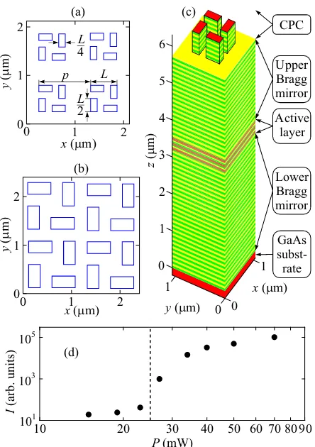
FIG. 1. (color online). (a,b) The schematics of chiral pho-tonic crystal (CPC) composed of a square lattice of rectan-gular nanopillars in Sample A (panel a) and B (panel b), 2×2 periods are shown. (c) The schematics of the unit cell of Sample A. The nanopillars, composing the CPC, are etched through the top 4.75 (of 23) Bragg pairs of the up-per Bragg mirror of a planar AlGaAs/AlAs microcavity with twelve GaAs QWs (three groups of four). Green and yellow colors represent AlAs and AlGaAs λ/4-layers, respectively. Red color represents GaAs substrate, smoothing layers be-tween Bragg pairs and active QWs. (d) Measured emission intensity of Sample A I as a function of the optical pump intensityP.
schematics of the CPC is depicted in Fig. 1, see also in Supplementary Material. It consists of a square lattice of rectangular pillars that have a broken in-plane mirror symmetry but possess a fourfold rotational axis and pos-sess the potential to demonstrate a strong optical activ-ity16. The vertical walls of nanopillars are normal to the [110] and [¯110] crystallographic directions. This structure has a C4 point symmetry, and it is three-dimensionally
chiral, because it does not have planes of mirror symme-try, including the horizontal one6.
Two different periodic structures (Sample A and B hereafter) have been fabricated, basing on the theoreti-cal theoreti-calculations explained below and shown schematitheoreti-cally in Figs. 1a and 1b. Sample A (panel a) has the period
p = 1060 nm and pillar feature size L = 544 nm, and Sample B (panel b) hasp= 1200 nm andL= 960 nm.
1 5190 1522 1 525 0.5
1
Energy (meV)
Intensity (arb. units)
1 472 1 473 1 474
0 0.5 1
Intensity (arb. units)
1521 1522 1523
0 0.2 0.4 0.6 0.8 1 Polarization degree Energy (meV)
(a) 6 -1
Wavenumber (10 cm )
1.2264 1.2272 1.2280
0 0.5 1
Intensity (arb. units)
(b) 6 -1
Wavenumber (10 cm )
1.1872 1.1881 1.1889
0 0.2 0.4 0.6 0.8 1 Polarization degree Energy (meV) + I -I x I y I rc rlin rS
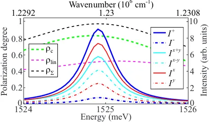
FIG. 2. (color online). (a) The emission intensity spectra of Sample A atT = 300 K at pump intensity above the thresh-old, atP≈2Pthr, in circularI±(blue solid and dash-dotted lines) and linearIx,y (red lines) polarizations. Green, ma-genta, and black lines with errorbars show the circular, linear, and total polarization degrees,ρc,ρlin,ρΣ, respectively. (b) Same for Sample B. The insert in panel (a) shows the emis-sion spectra in circular polarizationsI±in Sample A slightly below the threshold, atP = 0.95Pthr.
The horizontal size of chiral structure in each sample is approximately 50×50µm2. The Samples A and B are
cleaved from different horizontal parts of the wafer, and show different photon energies of the main MC mode, around 1523 and 1473 meV at room temperature, re-spectively.
The samples are held at room temperature. The exci-tation is carried out with a Ti-sapphire laser in the spec-tral range of the first reflection minimum of the MC. The laser spot has a diameter of about 10µm. The emission is collected in an angle range of±15◦. It is dispersed by a monochromator and detected by a Si CCD camera. The polarization of the luminescence is analyzed by a quarter wave retarder and linear polarizers.
The emission intensity from both samples at low pump intensities depends weakly on the angle, its spectral width reaches a few meV. With increase in the excita-tion power the emission spectrum and intensity show a threshold-like transition to lasing regime at P = Pthr,
see Fig. 1d for Sample A. Above the threshold the emis-sion line becomes narrow. The full width at half max-imum is about 0.23 meV at P = 1.1Pthr and increases
to∼0.5 meV at P = 2.5Pthr. Figures 2a and b display
[image:2.612.67.289.48.363.2] [image:2.612.327.551.52.283.2]15240 1525 1526 0.2
0.4 0.6 0.8 1
Energy (meV)
Polarization degree
0 2 4 6 8 10
Intensity (arb. units)
rc
rlin
rS
+
I
-I x+y I
x-y I
6 -1
Wavenumber (10 cm )
1.2292 1.23 1.2308
x I
y I
FIG. 3. (color online). Calculated (for Sample A) emission intensity spectra in right- and left-circular polarizations (thick blue solid and dash-dotted lines). The corresponding circular polarization degree spectra is shown by thick dashed green line. Red and cyan lines show the linearly polarized (inxyand diagonal directions respectively) intensitiesIx, Iy, Ix+y, Ix−y, calculated assuming that all oscillating dipoles are aligned along diagonalx+ydirection. The resulting linear and total polarization degreesρlin and ρΣ are shown as magenta and black dashed lines. It can be seen that the linear polarization is predominantly alongxdirection.
magnetic field. (The emission intensities in two diagonal linear polarizations x±y are not shown as they differ very weakly from each other.) The dashed lines in Figs. 2a and b show the degrees of circular, linear, and total polarization defined as
ρc=
I+−I−
I++I−, ρxy=
Ix−Iy
Ix+Iy, ρx±y=
Ix+y−Ix−y Ix+y+Ix−y, ρlin=
q ρ2
xy+ρ2x±y, ρΣ=
q ρ2
c+ρ2lin. (1)
It is seen that in Sample A the lasing is nearly com-pletely elliptically polarized, with polarization degrees at the intensity maxima as large asρc ∼80%, ρlin ∼50%,
and ρΣ ∼95% (Fig. 2a). The polarization of emission
in Sample B (Fig. 2b) is smaller,ρc ∼60%,ρlin ∼35%,
andρΣ∼80%. This is in agreement with a significantly
broader linewidth of the emission from Sample B, com-pare Figs. 2a and b.
The reciprocity and symmetry analysis of the structure shows that the CPC in the structures works as a wave-plate, exploring the Fabry-Perot interference between the vertically propagating modes in the slab, which allows reaching nearly a 100% circular polarization of the trans-mission11. To optimize the chiral structures for
obtain-ing a high DCP of light emission we have calculated the frequency dependence of emission in right and left cir-cular polarizations, using the optical scattering matrix and Fourier modal method10–12,17. In this approximation
the emission is calculated actually for homogeneously dis-tributed oscillating point dipoles in the QW plane, which are driven by external excitation and emit incoherently, so that the intensities rather than the electromagnetic fields are summed up at the receiver. This approximation (so called weak coupling limit) is not completely valid for
describing the lasing. But below and slightly above the threshold of the lasing regime it might be a reasonable starting point for optimization of the structures.
In this approximation, assuming the overall C4
[image:3.612.69.282.54.179.2]symme-try of the system, only a circular polarization of emission can be expected. The linear polarization is absent, be-cause the oscillating dipoles are assumed to be randomly linearly polarized in xy plane. The calculated emission intensities in right and left circular polarizationsI± for a structure with parameters of Sample A are shown in Fig. 3 as blue solid and dash-dotted lines. The intensi-ties are normalized to the emission intensity of the same oscillating dipoles in vacuum. The resulting dependence ofρc(~ω) is shown in Fig. 3 by the dashed green line. It can be seen that the emission is expected to be strongly circularly polarized, with ρc up to 80%, in agreement
with the experiment. For details on the simulated lin-early polarized components, see our explanations below, after discussion of the important features of the circular polarization control by CPC .
Additional insight into the mechanism of circularly po-larized emission is provided in Fig. 4 with the calcu-lated spatial distribution of the circularly polarized emis-sion intensity in Sample A at the resonant frequency ~ω = 1.522 eV, as well as the spatial distribution of the DCP of emission ρc(x, y), over the CPC unit cell.
We would like to emphasize that Fig. 5 does not show the emission intensity distributions in a certain plane above the sample, but the spatial distributions of the emission effectiveness from different spatial points of the sample unit cell in the normal direction of the structure. These spatial distributions are connected via the electro-dynamic reciprocity principle with the local electric field distributions in the active material plane inside the struc-ture, produced by a normally incident planar wave of the corresponding polarization11.
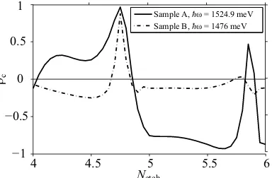
Note that ρc is very sensitive to the etching depth12.
Figure 5 shows the calculated dependence of the max-imum ρc of emission from Samples A (solid line) and
B (dash-dotted line) as functions of etching depthNetch
(measured in the number of etched Bragg pairs). Thus, the structures employed in our experiments withNetch∼
4.75 are in agreement with these calculations, corre-sponding to the maxima of the expectedρc.
Figure 2 shows that the measured emission in the las-ing mode shows as well a pronounced linear polarization alongxdirection in Fig. 1c, i.e., along the (110) crystallo-graphic direction of the AlGaAs and GaAs layers. There are two possible explanations: 1. The lasing operation itself, with possible preferential stimulated alignment of oscillating dipoles along a defined polarization direction. 2. The operation of the CPC, where possible fabrication-induced deformation of the CPC structures could lead to a reduced structural symmetry.
[image:3.612.64.297.393.440.2]I-( , )x y I+( , )x y rc( , ),x y <rc> =0.786
1
0.5
0
0.9 0.85 0.8 0.75 0.7 10.5
10 9.5 9 8.5 8 7.5 1.5
1
0.5 1
0.5
0 1
0.5
00 0.5 1 0 0.5 1 0 0.5 1
x( m)m
x( m)m
x( m)m
y
(m
)
m
y
(m
)
m
y
(m
)
m
FIG. 4. (color online). Calculated spatial emission intensity distributions in Sample A in left (I−(x, y)) and right (I+(x, y)) circular polarizations (left and central panels), and spatial distribution of circular polarization degreeρc(x, y) (right panel).
4 4.5 5 5.5 6
−1 −0.5
0 0.5
1
Netch
Sample A,hw= 1524.9 meV Sample B,hw= 1476 meV
rc
FIG. 5. Calculated dependencies of maximum circular po-larization degreeρcon etching depthNetch (measured as the number of etched Bragg pairs) for Sample A (solid line) and Sample B (dash-dotted line) structures.
intensities Ix,y, Ix±y in linear xy and diagonal
polariza-tions, assuming that all oscillating dipoles are aligned along diagonal x+y direction. The linear polarization degree ρlin and total polarization degree ρΣ are shown
as magenta and black dashed lines in Fig. 3. It is seen that the alignment of the oscillating dipoles leads to a pronounced linearxpolarization, as in the experiment.
As to the possible fabrication-induced deformation of the CPC structures, they may cause the linear polariza-tion of emission as well, see in Supplementary Material. However, the DCP in this case is usually less than in the perfect structure.
To conclude, we have found that fabricating chiral pho-tonic crystals with light emitting GaAs quantum wells inside a planar MC allows to realize lasing with a high degree of circular polarization of the light emission in the absence of a magnetic field. The advantage of using the CPCs with a large contrast of dielectric permittivities is its giant optical activity. This allows one to fabricate a very thin “waveplate”, with a thickness of the order of the emitted light wavelength. One more advantage of CPC half-wave plates lies in the fact that they, unlike the tra-ditional ones, have in-plane rotational isotropy due to the C4symmetry. Thus, our chiral structures do not require
linearly polarized emission of the active material at some
precise polarization direction, which is an important ad-vantage of the demonstrated approach over conventional quarter-wave plates.
Supplementary Material at [URL will be inserted by AIP] contains a more detailed description of the cavity design and the influence of possible fabrication-induced deformation of the CPC structures on the linear polar-ization of emission.
Acknowledgement. This work has been funded by Rus-sian Scientific Foundation (grant 14-12-01372) and State of Bavaria. We are grateful to K. Konishi, L. Kuipers, M. Kuwata-Gonokami, R. Oulton, H. Tamaru, and F. Capasso for fruitful discussions, and M. Emmerling for preparing the nanopillars.
[1] E. Yablonovitch, Phys. Rev. Lett.58, 2059 (1987).
[2] S. Fan, P. R. Villeneuve, J. Joannopoulos, and E. F. Schubert, Phys. Rev. Lett.78, 3294 (1997).
[3] E. Miyai, K. Sakai, T. Okano, W. Kunishi, D. Ohnishi, and S. Noda, Nature441, 946 (2006).
[4] A. Papakostas, A. Potts, D. M. Bagnall, S. L. Prosvirnin, H. J. Coles, and N. I. Zheludev, Phys. Rev. Lett.90, 107404 (2003). [5] M. Kuwata-Gonokami, N. Saito, Y. Ino, M. Kauranen, K. Jefi-movs, T. Vallius, J. Turunen, and Y. Svirko, Phys. Rev. Lett.
95, 227401 (2005).
[6] D.-H. Kwon, P. L. Werner, and D. H. Werner, Opt. Express
16, 11802 (2008).
[7] N. Liu, H. Liu, S. Zhu, and H. Giessen, Nat. Photon.3, 157 (2009).
[8] M. Hentschel, L. Wu, M. Sch¨aferling, P. Bai, E. P. Li, and H. Giessen, ACS Nano6, 10355 (2012).
[9] X. Yin, M. Sch¨aferling, B. Metzger, and H. Giessen, Nano Letters13, 6238 (2013)..
[10] A. A. Maksimov, I. I. Tartakovskii, E. V. Filatov, S. V. Lobanov, N. A. Gippius, S. G. Tikhodeev, C. Schneider, M. Kamp, S. Maier, S. H¨ofling, and V. D. Kulakovskii, Phys. Rev. B89, 045316 (2014).
[11] S. V. Lobanov, T. Weiss, N. A. Gippius, S. G. Tikhodeev, V. D. Kulakovskii, K. Konishi, and M. Kuwata-Gonokami, Opt. Lett.40, 1528 (2015).
[12] S. V. Lobanov, S. G. Tikhodeev, N. A. Gippius, A. A. Mak-simov, E. V. Filatov, I. I. Tartakovskii, V. D. Kulakovskii, T. Weiss, C. Schneider, J. Geßler, M. Kamp, and S. H¨ofling, Phys. Rev. B92, 205309 (2015).
[13] K. Konishi, M. Nomura, N. Kumagai, S. Iwamoto, Y. Arakawa, and M. Kuwata-Gonokami, Phys. Rev. Lett. 106, 057402 (2011).
[image:4.612.102.520.52.172.2] [image:4.612.78.270.225.351.2][15] P. Rauter, J. Lin, P. Genevet, S. P. Khanna, M. Lachab, A. Giles Davies, E. H. Linfield, and F. Capasso, Proceedings of the National Academy of Sciences111, E5623 (2014). [16] K. Konishi, B. Bai, X. Meng, P. Karvinen, J. Turunen, Y. P.
Svirko, and M. Kuwata-Gonokami, Opt. Express 16, 7189
(2008).