Transient Out-of-SOA Robustness of SiC Power
MOSFETs
Alberto Castellazzi, Asad Fayyaz
Power Electronics, Machines and Control GroupUniversity of Nottingham Nottingham, UK
Phone: +44-115-951-5568, e-mail: [email protected]
Gianpaolo Romano, Michele Riccio, Andrea Irace
Department of Electrical Engineering and Information TechnologyUniversity of Naples “Federico II” Naples, Italy
Jesus Urresti-Ibanez, Nick Wright
Department of Electrical and Electronic EngineeringNewcastle University Newcastle, UK
Abstract—Beyond their main function of high-frequency switches in modulated power converters, solid-state power devices are required in many application domains to also ensure robustness against a number of overload operational conditions. This paper considers the specific case of 1200 V SiC power MOSFETs and analyses their performance under three main transient regimes at the edge of and out of their Safe Operating Area: unclamped inductive switching led avalanche breakdown; short-circuit; operation as current limiting and regulating devices. The results presented highlight both inherent major strengths of SiC over Si and areas for improvement by tailored device design. The paper aims to contribute useful indications for technology development in future device generations to better match widespread and varied application requirements.
Index Terms-- Power MOSFET, Robustness, Semiconductor Device Reliability, Silicon Carbide, Wide Band Gap Semiconductors.
I. INTRODUCTION
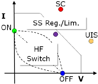
In a vast majority of power electronics applications, semiconductor devices are mainly meant to switch between an ON and an OFF state, which, for optimum efficiency, should entail as much as possible current flow without voltage drop and voltage blocking without current flow, respectively. The situation is illustrated with the help of Fig. 1, which shows a schematic summary of a power device operational conditions against its Safe Operating Area (SOA). The transition between the ON and OFF states can take place following various trajectories, aimed at shaping the switch performance
according to the needs (e.g., soft-switching techniques, resonant conversion). In reality, however, in a growing number of applications, devices are also expected to safely withstand a number of Out-of-SOA transient events, such as unclamped inductive switching (UIS), short circuit (SC) and, more and more, solid-state current regulation and limiting. Of interest are both the device single event withstand limits and its robustness and aging as a result of repetitive stress. It is typically very difficult, if not impossible, to predict how a given set of device characteristics will evolve over time and stress; so, operational points which are within or at the edge of the SOA at the time of design, may well fall outside of it at a later point in time and operational points outside of the SOA may see their equivalent excess stress increased in relation to the actual device limits.
[image:1.612.340.541.522.695.2]
Figure 1. Illustration of power device operation against its nominal SOA.
Silicon Carbide (SiC) is a relatively new technology for power devices and hitherto commercially available SiC power MOSFETs feature some characteristics which motivate a dedicated transient robustness study, in consideration of both technology inherent and design shapeable electro-thermal parameters. In the following, results are presented and discussed for the transistors robustness in the three above mentioned overload transient conditions. The MOSFETs under investigation are rated at 1.2 kV-80 mFor deeper insight into failure mechanisms and to assist the identification of pathways to enhanced robustness in future device generations, the methodology involves both functional and structural characterization using a balanced mix of experiment and 2D physical device electro-thermal simulation.
II. AVALANCHE RUGGEDNESS
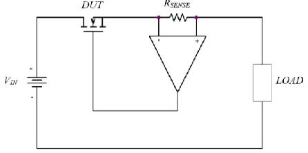
The energy dissipation limits of a power device in the avalanche breakdown regime are typically characterized by means of a UIS test, which reproduces representative operational conditions encountered, for instance, during load dumping and switching in the presence of parasitic inductance [1, 2]. A schematic of the corresponding test circuit is shown in Fig. 2 a): an inductor L is energized by turning-on a transistor T, connected in parallel to the device under test (DUT), which is kept turned-off;when T is switched off, the continuity requirement of the inductor current IL forces a
resonance process with the intrinsic output capacitance of T
and DUT to take place; provided that T is duly chosen with a higher breakdown voltage rating than the DUT, the latter is eventually driven into the avalanche breakdown regime, even for moderate values of IL and stored energy. It should be noted
that the use of T in parallel to DUT is not strictly necessary (i.e., DUT itself could be used for ramping up IL), but it helps
ensure that no self-heating takes place within DUT prior to the avalanche breakdown event.
a)
[image:2.612.329.555.270.580.2]b) Figure 2. UIS test circuit schematic, a), and representative ideal current and
voltage waveforms, b).
Ideal voltage and current waveforms for the test are shown in Fig. 2 b): when the process terminates safely, IL becomes zero
again and the drain source voltage, VDS, falls back to the input
source value VIN. The energy dissipated within the DUT is
(1)
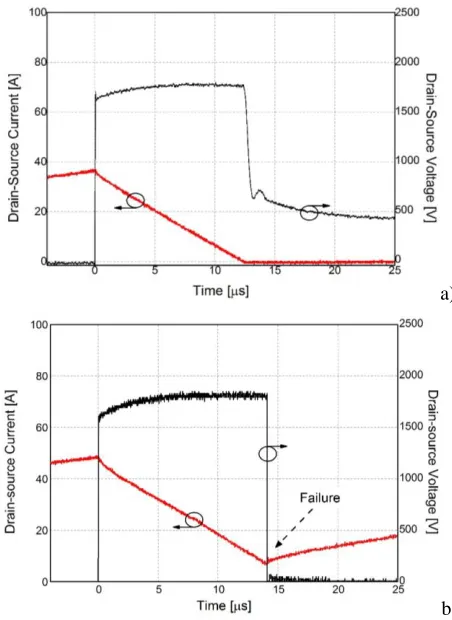
Fig. 3 shows experimental test results for both a safe and a destructive UIS test: typical signatures of failure, which is incurred here as a result of increased initial avalanche current value, are the rapid falling of VDS to zero rather than to VIN,
still before the inductor current has reached zero, and the sign inversion of the inductor current derivative, both clearly visible in Fig. 3 b). It should be noted that the actual breakdown voltage of the devices is much higher than the nominal specified rating of 1.2 kV, making it by definition an
Out-of-SOA type of transient.
a)
b)
Figure 3. In a), safe UIS and avalance breakdown event; in b), destructive event.
The phenomenon was thoroughly studied in Si MOSFETs. Failure is typically ascribed to activation of the parasitic n-p-n
[image:2.612.83.273.458.687.2]here of physical 2D electro-thermal device simulation. In particular, mixed-mode type simulations were carried out, with the device model structure and circuit arrangement shown in Fig. 4 a) and b), respectively. The model was validated statically and dynamically against data-sheet information up to a temperature of 150 ºC. Simulations were successful in qualitatively reproducing the experimental failure signatures of Fig. 3 b), as illustrated by the results reported in Fig. 5.
a)
[image:3.612.65.287.168.465.2]b) Figure 4. 2D simulation model structure, a); UIS circuit arrangement for
[image:3.612.347.518.209.525.2]mixed-mode simulations, b).
Figure 5. Simulated current and voltage waveforms for a destructive UIS and avalance breakdown event. Failure is defined as the moment where the voltage collapse takes place.
Fig. 6 shows a plot of the current density within the device during avalanche breakdown: in a), the current distribution away from failure is shown, whereas in b) the situation just
after failure detection (i.e., moment of abrupt decrease of VDS)
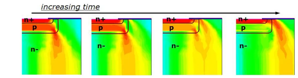
is illustrated. As can be seen, during safe avalanching, the current flows into the reverse body-diode of the transistor and its density peaks at the curvature of the p-n junction; however, at and after failure, the current has nearly entirely diverted to the channel and the region immediately underneath, without indications of bipolar transistor activation, even though a hole current continues to flow in the body. The current components during the event are detailed in Fig. 7: according to this model, shortly after the device enters the avalanche breakdown regime, a substantial electron current develops and increasingly contributes to the overall avalanche current, which consists entirely of electron current shortly after failure.
a)
b) Figure 6. Current density distribution during avalanche breakdown: in a), far
away from the time of failure; in b), just after filure.
[image:3.612.74.276.504.641.2] [image:3.612.344.527.566.703.2]Figure 8. Progressive re-distribution of the curent density within the device structure during the avalanche event, encompassing the time before and after failure.
The time evolution of the current density distribution is shown in Fig. 8, which clealry highlights a progressive shift of the conduction from the body-diode to the channel region, with a progressive transition from hole to electron current flow. This effect was interpreted as a result of the decrease of the threshold voltage with the consistent temperature increase around the p-body implant. An analytical estimate of its quantitative decrease supported this interpretation. Final experimental evidence was obtained by means of an additional UIS test with decreased value of DUT off-state bias voltage. Fig. 9 shows the UIS test results obtained for
VGS=0 and – 5V, respectively: in agreement with the
[image:4.612.326.554.389.605.2]interpretaiont of the failure mechanism given above, application of a negative bias on the DUT implies a later onset of the failure, corresponding to a longer time (i.e., a higeher temperature) needed before the threshold voltage decrease yields to channel activation.
Figure 9. UIS representative voltage and current waveforms for two different values of DUT off-state bias voltage.
III. SHORT-CIRCUIT WITHSTAND
For short-circuit withstand capability characterization, the circuit in Fig. 10 a) can be used: the DUT is biased with a constant voltage, VIN, of varying amplitude and driven with a
single pulse of varying duration; the DUT case temperature is typically also a test parameter. During the pulse, the current is limited only by the characteristics of the transistor and
typically reaches very high values. A representative drain current waveform, ID, is shown in Fig. 10 b). In this case, the
energy dissipated within the device is calculated as
(2)
where the drain-source voltage, VDS, can in most cases be
assumed constant, equal to VIN. An important difference of
SiC MOSFETs in relation, for instance, to Si IGBTs, is the relative value of the saturation current versus nominal on-state current, which is much higher in the former device type for all devices appeared on the market so far, involving significantly higher energy values in the event (see [3], for example).
a)
b) Figure 10. SC test circuit schematic, a), and representative current waveform,
b).
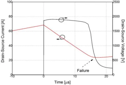
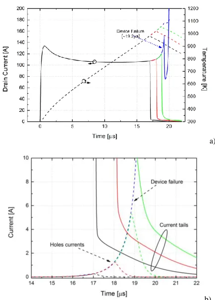
Fig. 11 shows experimental results of the short-circuit pulse at moderate bias voltage and temperature values, specified in the caption to the figure. As the pulse width is increased, two main observations are made: a change in slope of ID is observed, together with the appearance of turn-off
[image:4.612.69.285.441.593.2]shows evident signs of degradation, as highlighted by the dashed current profile reported in Fig. 11 (current waveform after degradation). Increasing the value of TCASE up to 150 °C, nominal rated temperature for the devices under test, only has the effect of reducing the time it takes for the same effects to be observed, but does not modify the failure signature.
Figure 11. SC current waveforms for VDS = 400 V, TCASE = 90 °C and varying
pulse width.
However, as VDS is progressively increased, the device
features a different failure signature, characterised by a noticeable reduction of its withstand capability and by catastrophic failure, without possibility of turning it off safely even for very small increments of the pulse, of the order of few tens of ns [4, 5]. Fig. 12 shows the experimental short-circuit current wavefom for VDS = 800 V and TCASE = 150 °C.
[image:5.612.77.289.141.296.2]
Figure 12. SC current waveforms for VDS = 400 V, TCASE = 90 °C. In this case, too, physical 2D device simulation was made use of to gain further insight. The simulation model is as shown in Fig. 4 a). The simulation test circuit only differs from that of Fig. 4 b) only for the removal of the load inductor
L. Fig. 13 summarizes some simulation results which well reproduce the experimental observations for the case of moderate VDS values. As detailed in Fig. 13 b), which shows a
zoom of Fig. 13 a) around the current tails, hole current components add to the electron ones and contribute to determine the device failure as their value is progressively allowed to increase.
a)
b) Figure 13. Simulated current waveforms for the SC event, with reconstruction of experimentally observed change of current slope and appearance of current tails.
Fig. 14 illustrates the distribution of the two current components within the device: the electron currents remain essentially confined to the channel, whereas the hole current components flow as reverse-diode current, reaching high densities in the region just underneath the channel. As the current density and temperature increase beyond a given value, a thermal runaway condition is entered, which leads to catastrophic failure. Here, too, no evidence of parasitic BJT activation is however observed.
[image:5.612.94.287.422.568.2] [image:5.612.330.535.511.689.2]In simulation, too, as the value of VDS is increased further, the device goes straight into a catastrophic failure mode, characterized by reverse hole current induced thermal runaway [6].
[image:6.612.333.556.108.219.2]Summarizing, the short circuit failure is interpreted on the basis of the achievement within the device of two different temperature thresholds, as illustrated in Fig. 15: if power dissipation in the device is such that the temperature trespasses a given lower temperature value (TDEG) of a sufficient length of time, then permanent degradation is incurred, but not necessarily catastrophic failure; according to all evidence, TDEG is already associated with the flow of reverse hole current components, but not such as to cause a thermal runaway. If however, the heat generation rate is increased and the temperature reaches a higher threshold (TTH_RNW), then a thermal runaway condition is entered, with catastrophic failure of the device. The interpretation proposed here finds further experimental evidence in [7]: measurements of gate current and gate-source voltage clearly reveal major increase of gate leakage current components in presence of the moderate failure only, while chip infrared thermal mapping in the two situations clearly shows that, while the temperature remains homogeneously distributed in the moderate type of degradation, hot spots are on the other hand clearly detected in the case of thermal runaway. The energy values involved in determining one or the other failure type can differ appreciably.
Figure 15. Summary of SC failure mechanism in relation to the heat-generation rate and temperature increase within the chip.
IV. CURRENT LIMITING AND REGULATION CAPABILITY
There is an interest in using transistors as current limiting and regulating elements at the output of a power supply, for instance when charging a capacitive load or during an overload or faulty condition or in repetitive pulsed-power type applications [8]. The situation is illustrated with the simplified circuit schematic of Fig. 16: in this operational mode, the device typically has to withstand a high VDS, while the driving
gate-source voltage, VGS, is however not constant, but is
changed (typically, decreased) in real time against variations in current and temperature within the device to try and keep the current level or rate-of-rise thereof constant. The event can
[image:6.612.67.284.369.551.2]be extremely dissipative, with energy levels calculated according to Eq. 2 and so, the higher temperature capability of SiC makes it an attractive alternative over Si.
Figure 16. Test circuit schematic for device use as current limiter and regulator.
However, the fact that VGS can in principle span the whole
range (e.g., -5 to + 20 V for SiC MOSFETs) during the transient implies the possibility of the device entering a thermally unstable operational bias condition. Indeed, depending on the applied VGS and VDS, power MOSFETs
exhibit two different regions of operation, defined by the relative temperature dependence and value of the threshold voltage, Vth, and electron mobility, . For high values of VGS,
the decrease of mobility with temperature is the dominating factor and the devices exhibit stable temperature behavior, characterized by a negative temperature coefficient of the drain current ; conversely, at lower VGS values, the
decrease of Vth with temperature prevails, leading to thermally
unstable operation, with the current increasing with temperature. A representative current waveform under thermally unstable bias conditions is plotted in Fig. 17, for the case of constant VGS applied. Operation under such bias
conditions is associated with uneven current and power distribution within the chip, current crowding and hot-spot formation [6, 9], resulting in a very stressful effectively out-of-SOA operational mode. Failure to the achievement of a highly localized excessive temperature.
Figure 17. SiC MOSFET current waveform under thermally unstable bias conditions (here: VDS = 150 V; VGS = 7.5 V; TCASE = 25 °C) Though significant improvements have taken place over subsequent generations, most latest-generation commercial SiC power MOSFETs still feature a relatively broad region of thermally unstable bias (see Fig. 18, for example) [3].
If VGS is varied in real time with a sense on the drain
[image:6.612.332.544.515.598.2]Figure 18. Transfer-characteristics of a new generation 1200V SiC MOSFET as per data-sheet information [3].
[image:7.612.73.279.563.696.2]a constant value for some time before the onset of instability [10, 11]. The ability of the device to safely withstand operation in this regime needs thorough analysis of Tand of
its transient evolution during the current limiting event. Indeed, denoting with PHEAT the power dissipation within the
device and with PCOOL the amount of heat extracted by
cooling, on-set of thermal instability requires that
(3)
which, for a given value of VDS can be re-written as
(4)
So, depending on the bias and temperature values, different situations can occur, as summarized in Fig. 19 [6, 9, 10]. In relation to SiC devices, it is interesting to note that the ID
range of thermally unstable behavior decreases with increasing temperature [6, 9, 12]. In view of the small die sizes and relatively high thermal conductivity of SiC, together with its high temperature withstand capability, the technology offers the potential to design devices which are robust as current limiters in transient operation. The key aspect to be investigated is the transient variation of T with temperature
Figure 19. Qualitative summary illustration of thermally unstable operation onset depending on device bias and structural characteristics.
at different bias conditions, against a given chip thermal impedance. Device simulation relying on traditional tools is challenging in view of the required large size multi cell structure required to investigate the problem. Novel simulation approaches optimizing the trade-off between accuracy and computational efficiency in the coupled functional and structural device characterization can be a very valid support tool for these kind of investigations [13]-[16].
V. CONCLUSION
This paper has proposed a review of the failure mechanisms of SiC power MOSFETs in three main transient out-of-SOA operational regimes. Other publications have already provided numerical quantification of the energy associated with failure in the various regimes, as well as the impact of repetitive pulse stress application on the device aging. As far as the avalanche ruggedness is concerned, it can be undoubtedly concluded that SiC MOSFETs perform excellently [4, 17], offering yet another asset over their Si counterparts. No evidence of parasitic BJT activation is found and the failure could be delayed further by achieving a lower turn-off bias voltage in future generations. On the other hand, the relatively high saturation current of hitherto presented device concepts implies higher than ideal energy and stress levels involved in short-circuit events, to the detriment of the maximum pulse duration [5, 18]. The implication is twofold: fast fault detection and removal circuits are needed and aging due to repetitive stress can be pronounced even if the faulty condition is promptly removed. This is particularly relevant in consideration of the rather large margin that still exists between the nominal and the actual breakdown voltage rating of most devices: the devices considered in this study have an actual breakdown voltage of around 1.8 kV, for a nominal specification of 1.2 kV. This indicates the likelihood that future generation higher voltage devices (e.g. 1.5 or 1.7 kV MOSFETs) may not differ significantly from the 1.2 kV ones in terms of their design, but will be requested to withstand short-circuit operation at much higher voltage levels (i.e., even higher heat-generation rates) than the 1.2 kV MOSFETs. Similarly to what has happened with Si devices, it is to be expected that the maximum short-circuit withstand capability will become an important figure of merit and selection criteria for a number of applications (particularly, motor drives). In view of the highlighted failure mechanisms, device design for improved robustness should target saturation current reduction and further improvement of the gate-oxide. Finally, a conclusive assessment of the devices suitability to be employed as current limiters and regulators requires further analysis and testing, but issues related to the device characteristics (e.g., transfer characteristics) are evident, in particular in relation to the implementation of parallel multi-chip structures for higher current ratings. An improvement in the transfer characteristics has been observed in the past few years among subsequent generations and it appears that current limiting capability can be further improved by design.
ACKNOWLEDGMENT
REFERENCES
[1] A. Fayyaz, J. Urresti, G. Romano, M. Riccio, A. Castellazzi, A. Irace, N. Wright, “UIS Failure Mechanism of SiC Power MOSFETs”, in
Proc. 4th Annual IEEE Workshop on Wide Bandgap Power Devices and Applications, Fayetteville, Arkansas, USA – Nov. 8th, 2016. [2] M. Nawaz, “Evaluation of SiC MOSFET power modules under
unclamped inductive switching test environment”, Microelectronics Reliability Vol. 63, August 2016, Pages 97–103.
[3] Wolfspeed, Research Triangle Park, NC, USA. “C2M0080120D: data-sheet” [Online]. Available: http://www.wolfspeed.com/media/downloads/167/C2M0080120D.pdf [4] A. Fayyaz, L. Yang, A. Castellazzi, “Transient robustness testing of
silicon carbide (SiC) power MOSFETs”, in Proc. 15th European Conference on Power Electronics and Applications (EPE2013), Lille, France, September 2013.
[5] A. Fayyaz, L. Yang, A. Castellazzi, M. Riccio, A. Irace, “Short-circuit robustness of SiC Power MOSFETs: experimental analysis”, in Proc. of the 26th IEEE International Symposium on Power Semiconductor Devices & IC's (ISPSD2014), June 15-19, 2014 Waikoloa, Hawaii. [6] A. Castellazzi, A. Fayyaz, G. Romano, M. Riccio, A. Irace, “SiC power
MOSFETs performance, robustness and technology maturity”,
Microelectronics Reliability – Special Issue on “Reliability Issues in Power Electronics”, Vol. 58, March 2016, Pages 164–176.
[7] G. Romano, A. Fayyaz, M. Riccio, L. Maresca, G. Breglio, A. Castellazzi, A. Irace, “A Comprehensive Study of Short-Circuit Ruggedness of Silicon Carbide Power MOSFETs”, IEEE Journal of Emerging and Selected Topics in Power Electronics, Vol. 4, No. 3, Sep. 2016
[8] C. Gu, P. Wheeler, A. Castellazzi, A. J. Waston, F. Effah, “A Survey on Configurations of Current-Limiting Circuit Breakers (CL-CB)”, in
Proc. 18th European Conference on Power Electronics and Applications (EPE'16 ECCE Europe), Karlsruhe, Germany, 5-9 Sept. 2016.
[9] M. Riccio, A. Castellazzi, G. De Falco, A. Irace, “Experimental analysis of electro-thermal instability in SiC Power MOSFETs”,
Microelectronics Reliability, Vol. 53, Issues 9–11, September– November 2013, Pages 1739–1744.
[10] P. Spirito, G. Breglio, V. d'Alessandro, N. Rinaldi, “Analytical Model for thermal instability of low voltage power MOS and S.O.A in pulse operation”, in Proc. of the 14th IEEE International Symposium on Power Semiconductor Devices and ICs (ISPSD2002), Santa Fe, New Mexico, USA, June 2002.
[11] A. Castellazzi, M. Ciappa, “Electrothermal characterization for reliability of modern low-voltage power MOSFETs”, IEEE Trans. On Device and Materials Reliability, Vol. 7, No. 4, Dec. 2007.
[12] A. Castellazzi, T. Funaki, T. Kimoto, T. Hikihara, “Thermal instability effects in SiC Power MOSFETs”, Microelectronics Reliability, Vol. 52, Issues 9–10, September–October 2012, Pages 2414–2419.
[13] V. d’Alessandro et al., “SPICE Modeling and Dynamic Electrothermal [14] Simulation of SiC Power MOSFETs”, in Proc. of the 26th IEEE
International Symposium on Power Semiconductor Devices & IC's (ISPS2014), June 15-19, 2014 Waikoloa, Hawaii.
[15] R. Kraus, A. Castellazzi, “A Physics-Based Compact Model of SiC Power MOSFETs”, IEEE Trans. on Power Electronics, Vol. 31, No. 8, Aug. 2016.
[16] L. Codecasa, V. d’Alessandro, A. Magnani, A. Irace, “Circuit-Based Electrothermal Simulation of Power Devices by an Ultrafast Nonlinear MOR Approach”, IEEE Trans. on Power Electronics, Vol. 31, No. 8, Aug. 2016.
[17] A. Fayyaz, , L. Yang, M. Riccio, A. Castellazzi, A. Irace, “Single pulse avalanche robustness and repetitive stress ageing of SiC power MOSFETs”, Microelectronics Reliability, Vol. 54, Issues 9–10, September–October 2014, Pages 2185–2190.
![Figure 18. Transfer-characteristics of a new generation 1200V SiC MOSFET as per data-sheet information [3]](https://thumb-us.123doks.com/thumbv2/123dok_us/8567084.367382/7.612.73.279.563.696/figure-transfer-characteristics-generation-sic-mosfet-sheet-information.webp)
