Prepared for submission to JINST
Ionization Electron Signal Processing
in Single Phase LArTPCs
I. Algorithm Description and
Quantitative Evaluation with MicroBooNE Simulation
MicroBooNE Collaboration
C. AdamsiR. Anj J. AnthonycJ. Asaadiaa M. AugeraL. BagbyhS. Balasubramanianee B. BallerhC. BarnespG. Barrs M. Basss,bF. Baybb A. Bhatx K. Bhattacharyat M. Bishaib A. BlakelT. Boltonk L. CamillerigD. CaratelligR. Castillo FernandezhF. CavannahG. Ceratih H. ChenbY. ChenaE. ChurchtD. CiancigE. CohenyG. H. CollinoJ. M. ConradoM. Converyw L. Cooper-TroendleeeJ. I. Crespo-AnadóngM. Del TuttosD. DevittlA. DiazoS. Dytmanu B. EberlywA. EreditatoaL. Escudero Sanchezc J. EsquivelxJ. J. EvansnA. A. Fadeevag B. T. FlemingeeW. ForemandA. P. FurmanskinD. Garcia-GameznG. T. GarveymV. Gentyg D. GoeldiaS. Gollapinniz E. GramellinieeH. GreenleehR. Grossoe R. Guenettes,i
P. GuzowskinA. HackenburgeeP. HamiltonxO. HenoJ. HewesnC. HillnJ. Hod G. A. Horton-Smithk A. HourlieroE.-C. HuangmC. JameshJ. Jan de Vriesc L. Jiangu R. A. Johnsone J. JoshibH. JostleinhY.-J. JwagD. KalekogG. KaragiorgigW. Ketchumh B. Kirbyb M. KirbyhT. KobilarcikhI. KresloaY. LibA. ListerlB. R. Littlejohnj S. Lockwitzh D. LorcaaW. C. LouismM. LuethiaB. LundberghX. LuoeeA. MarchionnihS. Marcoccih C. MarianiddJ. MarshallcD. A. Martinez CaicedojA. Mastbaumd V. MeddagekT. Miceliq G. B. MillsmA. Moganz J. MoonoM. Mooneyb,f C. D. MoorehJ. MousseaupM. Murphydd R. MurrellsnD. NaplesuP. Nienaberv J. NowaklO. PalamarahV. PandeyddV. Paoloneu A. PapadopoulouoV. PapavassiliouqS. F. PateqZ. PavlovichE. Piasetzkyy D. Porzion G. PulliamxX. QianbJ. L. RaafhV. RadekabA. RafiquekL. Rochesterw M. Ross-Lonergang C. Rudolf von RohraB. RusselleeD. W. SchmitzdA. SchukrafthW. Seligmang
M. H. ShaevitzgJ. SinclairaA. Smithc E. L. SniderhM. Soderbergx S. Söldner-Remboldn S. R. Soletis,iP. SpentzourishJ. SpitzpJ. St. Johne,hT. StrausshK. Suttong
S. Sword-FehlbergqA. M. SzelcnN. Taggr W. Tangz K. Teraog,wM. Thomsonc C. Thornb M. ToupshY.-T. Tsaiw S. TufanlieeT. UsherwW. Van De Pontseeles,iR. G. Van de Waterm B. VirenbM. WeberaH. WeibD. A. WickremasingheuK. Wiermant Z. Williamsaa S. Wolbersh T. Wongjirado,ccK. Woodruffq T. YanghG. Yarbroughz L. E. YatesoB. YubG. P. Zellerh J. ZennamodC. Zhangb
aUniversität Bern, Bern CH-3012, Switzerland
bBrookhaven National Laboratory (BNL), Upton, NY, 11973, USA cUniversity of Cambridge, Cambridge CB3 0HE, United Kingdom dUniversity of Chicago, Chicago, IL, 60637, USA
eUniversity of Cincinnati, Cincinnati, OH, 45221, USA fColorado State University, Fort Collins, CO, 80523, USA gColumbia University, New York, NY, 10027, USA
hFermi National Accelerator Laboratory (FNAL), Batavia, IL 60510, USA iHarvard University, Cambridge, MA 02138, USA
jIllinois Institute of Technology (IIT), Chicago, IL 60616, USA kKansas State University (KSU), Manhattan, KS, 66506, USA
lLancaster University, Lancaster LA1 4YW, United Kingdom
mLos Alamos National Laboratory (LANL), Los Alamos, NM, 87545, USA nThe University of Manchester, Manchester M13 9PL, United Kingdom oMassachusetts Institute of Technology (MIT), Cambridge, MA, 02139, USA pUniversity of Michigan, Ann Arbor, MI, 48109, USA
qNew Mexico State University (NMSU), Las Cruces, NM, 88003, USA rOtterbein University, Westerville, OH, 43081, USA
sUniversity of Oxford, Oxford OX1 3RH, United Kingdom
tPacific Northwest National Laboratory (PNNL), Richland, WA, 99352, USA uUniversity of Pittsburgh, Pittsburgh, PA, 15260, USA
vSaint Mary’s University of Minnesota, Winona, MN, 55987, USA wSLAC National Accelerator Laboratory, Menlo Park, CA, 94025, USA
xSyracuse University, Syracuse, NY, 13244, USA yTel Aviv University, Tel Aviv, Israel, 69978
zUniversity of Tennessee, Knoxville, TN, 37996, USA aaUniversity of Texas, Arlington, TX, 76019, USA
bbTUBITAK Space Technologies Research Institute, METU Campus, TR-06800, Ankara, Turkey ccTufts University, Medford, MA, 02155, USA
ddCenter for Neutrino Physics, Virginia Tech, Blacksburg, VA, 24061, USA eeYale University, New Haven, CT, 06520, USA
E-mail: [email protected]
Abstract: We describe the concept and procedure of drifted-charge extraction developed in the MicroBooNE experiment, a single-phase liquid argon time projection chamber (LArTPC). This technique converts the raw digitized TPC waveform to the number of ionization electrons passing through a wire plane at a given time. A robust recovery of the number of ionization electrons from both induction and collection anode wire planes will augment the 3D reconstruction, and is particularly important for tomographic reconstruction algorithms. A number of building blocks of the overall procedure are described. The performance of the signal processing is quantitatively evaluated by comparing extracted charge with the true charge through a detailed TPC detector simulation taking into account position-dependent induced current inside a single wire region and across multiple wires. Some areas for further improvement of the performance of the charge extraction procedure are also discussed.
Contents
1 Introduction 2
2 LArTPC signal formation 4
2.1 Field response 4
2.2 Electronics response 10
2.3 Topology-dependent TPC signals 12
3 Reconstruction of drifted electron distribution 14
3.1 Signal extraction principles 15
3.1.1 Deconvolution and software filters 18
3.1.2 2D deconvolution 19
3.1.3 Region of interest (ROI) 20
3.2 Method 22
3.2.1 Position-averaged response functions 23
3.2.2 Software filters 24
3.2.3 Identification of signal ROIs 26
3.2.4 Refinement of ROIs 29
4 Evaluating TPC signal processing with simulation 31
4.1 Key simulation improvements 32
4.2 Simulation overview 33
4.2.1 Initial distribution of charge depositions 35
4.2.2 Drift transport and physics 35
4.2.3 Detector field and electronics response 36
4.2.4 Performing the convolution 37
4.2.5 Truth values 39
4.2.6 Noise simulation 39
4.3 Quantitative evaluation of the signal processing 41
4.3.1 Basic performance of the signal processing 42
4.3.2 Charge resolution due to electronics noise 43
4.3.3 Charge bias due to thresholding in ROI finding 45
4.3.4 Inefficiency of line charge extraction 46
4.3.5 Performance of line charge extraction 46
5 Discussion 47
5.1 Limitations of 2D field responses 48
5.2 Limitations of the current ROI finding 52
6 Summary 53
1 Introduction
The liquid argon time projection chamber (LArTPC) [1–4] is an innovative detector technology being actively developed worldwide. Several features of the LArTPC make it well adapted to the study of neutrinos and other rare processes. Argon is readily available commercially (∼1 % by volume, the most abundant noble gas in the atmosphere). Free electrons have high mobility, low diffusion [5], and very high survival time in pure liquid argon (LAr), making it an attractive material for a TPC. In addition, LAr has a relatively high density and a high scintillation light yield. In the near term, the Short-Baseline Neutrino Program [6] will utilize three LArTPCs (MicroBooNE, SBND, and ICARUS) at Fermi National Accelerator Laboratory (Fermilab) to search for eV-scale sterile neutrino(s) and measure neutrino-argon interaction cross sections. In the long term, the long-baseline Deep Underground Neutrino Experiment (DUNE) [7] is planning to use four large 10 kilotons LArTPC modules as far detectors to search for leptonic CP violation, determine the neutrino mass hierarchy, test the standard three-neutrino paradigm, search for proton decays, and potentially observe supernova neutrino bursts. The development of high-quality and fully-automated event reconstruction algorithms for LArTPC neutrino detectors is crucial to the success of the short-baseline and long-short-baseline physics programs and is an area of significant activity [8–11]. The robust recovery of the ionization signals from the LArTPC images is the critical first stage of LArTPC reconstruction.
The MicroBooNE detector [12] is the first LArTPC in the Short-Baseline Neutrino Program [6] to be operational. It is a single-phase LArTPC built to observe interactions of neutrinos from the on-axis Booster [13] and off-axis NuMI [14] beams at Fermi National Accelerator Laboratory in Batavia, IL. The TPC LAr volume is 2.56 m× 2.3 m×10.4 m with 89 metric tons active mass, housed in a foam-insulated evacuable cryostat vessel. At the anode end of the 2.56 m drift distance, there are three parallel wire readout planes [15]. The first wire plane facing the cathode is labeled "U", and the second and third plane are labeled "V" and "Y", respectively. The wire pitch and the gap between two adjacent wire planes are both 3 mm. The 3456 wires in the Y plane are oriented vertically. The U and V planes each contain 2400 wires oriented ±60◦ with respect to vertical. Behind the wire planes and external to the TPC, there is an array of 32 photomultiplier tubes [16] to detect scintillation light for triggering, timing, and other purposes.
Cathode Plane
Edrift
U V Y Liquid Argon TPC
Y wire plane waveforms
V wire plane waveforms Sense Wires
t Incoming Neutr
ino
[image:5.595.105.520.129.428.2]Charged Particles
Figure 1: Diagram illustrating the signal formation in a LArTPC with three wire planes [12]. The signal on each plane produces a 2D image of the event. For simplicity, the signal in the U induction plane is omitted from the diagram.
on a wire of the Y plane as all nearby ionization charge is collected. The U and V wire planes are commonly referred to as the induction planes. Although also measuring induced current, the Y wire plane is commonly referred to as the collection plane.
While the collection plane signal is mostly unipolar and large in amplitude with a Gaussian time profile, the induction plane signal is bipolar and small in amplitude with a complex time profile. The latter is due to the overlapping of many bipolar signal shapes as a distribution of drifting charge passes near the wires. Despite complications in the induction plane signal, the combination of the induction and collection wire planes is essential for tomographic event reconstruction [11] in single-phase LArTPCs. Leveraging the induction signal in combination with the collection signal is important to fully exploit single-phase LArTPC capabilities.
this alternative scheme for large detectors is not actionable at present, though good progress has been made [18]. If the wire readout in MicroBooNE were replaced by a full 2D pixel readout, the total number of channels would be 2.7 million instead of 8,256, resulting in a significant increase in the cost of electronics. Furthermore, the power consumption of these electronics inside LAr would be a serious concern. Given the wire readout technology employed in the single-phase LArTPCs, reconstruction of the charge passing through the induction wire plane improves the correlation of signal between the multiple anode plane views and helps resolve degeneracies inherent in a projective wire geometry.
The successful reconstruction of a 3D event topology generally requires robust signal extraction in multiple 2D projection views. Since the ionization electrons are not collected on any of the induction wire planes, they naturally provide additional non-destructive views of the ionization electrons from the charged particle tracks. A successful extraction of the ionization electron information from the complicated induction plane signals is essential for 3D event reconstruction in single-phase LArTPCs using tomographic reconstruction and is expected to further enhance 3D reconstruction for techniques that match the image in different 2D projection views.
This paper is organized as follows. In section2, we review the process of TPC signal formation including the induced current generation, signal amplification and shaping, as well as the impact of noise. In section3, we describe the principle and the algorithm implemented to extract ionization charge from the TPC signal. The performance of the TPC signal processing chain is then evaluated with a detailed TPC simulation in section 4. The assessment of this signal processing technique on MicroBooNE data is provided in a dedicated accompanying paper [19]. A discussion of some identified limitations of the current techniques is in section5. A summary and prospects for future improvements are presented in section6.
2 LArTPC signal formation
The formation of the TPC signal consists of three parts: i) the electric field response to the drifting of a point ionization charge leading to induced currents on the sense wires, ii) the electronics response to the induced current waveform input to each channel in terms of amplification and shaping, and iii) the initial distribution of the ionization charge in the bulk of the detector, how this charge drifts in the applied electric field and how it undergoes diffusion and absorption as it drifts. In the following sections, we describe each part in detail.
2.1 Field response
When ionization electrons drift past the initial two induction wire planes toward the final collection wire plane, current is induced on nearby wires. Henceforth, we refer to the induced current on one wire due to a single electron charge as a field response function. The principle of current induction is described by Ramo’s theorem [20]. An element of ionization charge q in motion at a given location induces a currention some electrode (wire),
i=−qE®w · ®vq. (2.1)
This current is proportional to the inner product of a constructed weighting field E®
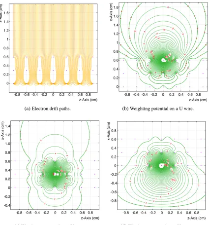
depends on the geometry of the electrodes and can be calculated by removing the drifting charge, placing the targeted electrode at unity potential, and setting all other conductors to ground. For a single medium, the weighting potential is independent of the dielectric properties/constants. For multiple media, the weighting potential must be calculated taking into account each material’s dielectric properties. This result is valid in the quasi-static approximation and in arbitrary linear media where the permittivity is independent of the potentials [21,22]. A generalized form of the weighting potential considering non-linear effects can also be found in [21] and [22]. The charge’s drifting velocity®vqis a function of the external electric field, which depends on the geometry of the electrodes as well as the applied drifting and bias voltages and liquid argon temperature. Figure2
shows electron drift paths in an applied electric field as well as lines of equal potentials for the weighting field for the U, V, and Y wire planes in MicroBooNE. The electron drift paths and the weighting fields are calculated using the Garfield [23] software. These calculations adopt a 2D model of a portion of MicroBooNE near a subset of wires. Some limitations in this model are discussed in section5.1.
Although equation 2.1fully describes a field response function for a given point charge at a given moment in time, the easiest way to understand the qualitative behavior of the field response function is through the integral of the induced current and its connection to Green’s reciprocity theorem. Let’s consider a case where a point chargeqmis moving in an inter-electrode space. If we then assume that the chargeqmis on an infinitesimal electrode and the sensing electrode is labeled as electrode I, then by Green’s reciprocity,
qm·Vm=QI ·VI. (2.2)
HereQI is the charge on the sensing electrode induced byqm.Vmis the potential at the location of qmintroduced by the sensing electrode potentialVI. With equation2.2, we can derive the induced current as
i= dQI
dt =qm· ®∇Vw · dr®
dt, (2.3)
where the weighting potential1is a dimensionless quantity defined asVw =Vm/VI. It is easy to see that the above equation recovers equation2.1where∇®V
wcorresponds to− ®Ewandd®dtr is the velocity of the chargeqm. Given equation2.3, the integral of the induced current due to a chargeqmmoving along its drift path
∫
idt =qm·
Vwend−Vwst ar t
(2.4)
is proportional to the difference of the weighting potential at the end and start of the path.
For signal processing and signal simulation, the field response functions for a single ionization electron traveling over a number of possible discrete drift paths are calculated with the Garfield program [23] using a 2D model for MicroBooNE wires with a scheme illustrated in figure3. The calculation utilizes a region that spans 22.4 cm (the upper boundary at 20.4 cm in front of the Y plane) along the nominal electron drift direction and 30 cm perpendicular to both the drift direction and the wire orientation. In the calculation, each wire plane contains 101 wires with 150 µm diameter separated by a 3 mm wire pitch. The drifting field (273 V/cm) is achieved by setting the
1This is equivalent to the definition from Ramo’s theorem, where the voltage on the electrode under consideration is
1.6
1.4 1.2
1
0.8
0.6
0.4 0.2
0
-0.8 -0.6 -0.4 -0.2 0 0.2 0.4 0.6 0.8
z-Axis (cm)
x-Axis (cm)
(a)Electron drift paths.
1.8
1.6
1.4
1.2 1
0.8
0.6
0.4
0.2
0
-0.8 -0.6 -0.4 -0.2 0 0.2 0.4 0.6 0.8
z-Axis (cm)
x
-Axis (cm)
(b)Weighting potential on a U wire.
1.4
1.2
1.0
0.8
0.6
0.4
0.2
0
-0.2
-0.4
x
-Axis (cm)
-0.8 -0.6 -0.4 -0.2 0 0.2 0.4 0.6 0.8
z-Axis (cm)
(c)Weighting potential on a V wire.
-0.8 -0.6 -0.4 -0.2 0 0.2 0.4 0.6 0.8
z-Axis (cm)
0.8 0.6
0.4
0.2 0
-0.2
-0.4 -0.6
-0.8
x
-Axis (cm)
[image:8.595.88.514.115.572.2]negative voltage at the upper boundary of the simulated area. The nominal MicroBooNE operating bias voltages for each wire plane are used in the calculation.
There are two stages in calculating the field response functions. The first one is the calculation of the electron drift paths in the applied electric field as shown in figure2a. The second stage is the calculation of the weighting electric potentials as shown in the remaining panels of figure2. The induced current can be calculated following equation (2.1). The electron drift velocity as a function of electric field is taken from recent measurements [5,24]. For these single-electron simulations, diffusion is omitted.
3 mm
3 mm Diameter 150 um
U
V
Y
- 110V 0 V
+230 V 3 mm
-10 wire 0 wire +10 wire
electron
10 cm
E
shift
10 cm shift electron
1.5 mm
0.3 mm
Figure 3: Illustration of the 2D Garfield simulation scheme (dimensions not to scale), where black dots indicate individual wires. MicroBooNE’s anode plane-to-plane spacing is 3 mm, with 3 mm wire pitch in each plane. The inset denotes the sub-pitch designation of electron drift paths whereupon the field response is calculated.
the MicroBooNE readout electronics.
The normalization of the overall response function is chosen so that the integral of the response function of the closest wire from the collection Y plane is unity, which corresponds to a single electron. To emphasize the shape of the field response functions, a special scale labeling with “Log10” is used to set the color scale of the induced currenti(electrons per 0.5 µs) in Figure4:
iin “Log 10” =
log10(i·105), ifi >1×10⁻⁵,
0, if −1×10⁻⁵ ≤i≤ 1×10⁻⁵, −log10(−1·i·105) ifi <−1×10⁻⁵.
(2.5)
The 2D nature of the model used for MicroBooNE wire planes in the Garfield calculation described above is an approximation of the actual detector. No detector edge effects are considered and the 2D nature of the model implies that wires are effectively infinite in length and that any effects due to the wires crossing near each other can not be included. An initial set of field calculations has been performed with custom software that utilizes a 3D model of the MicroBooNE wire planes. More discussions can be found in section5.1.
Given the results shown above, we can conclude the following:
• As an ionization electron moves towards the closest induction plane wire, it climbs up the cor-responding induction wire weighting potential; therefore, the induced current is negative and corresponds to the positive voltage waveform shown in this paper following the MicroBooNE electronics readout convention.
• As an ionization electron passes the induction wire plane and moves toward the collection wire plane, the induction wire weighting potential decreases and the induced current changes sign. This results in the bipolar shape for the induction plane signals. See examples in figure5.
• As an ionization electron drifts towards the wire on which it will eventually be collected (the central wire), the weighting function for that wire always increases. Consequently, collection wire signals are unipolar in shape.
• For an ionization electron originating from the cathode plane (i.e. weighting potential zero), the integrated induction charge in an induction wire plane is nominally zero, since the electron ultimately ends up at a collection wire for which the corresponding induction wire weighting potential is also zero. Similarly, the integrated induction charge in the collection wire should be equal to the charge of one electron, as the corresponding collection wire weighting potential is unity.
Wire Number 10
− −5 0 5 10
s] µ Time [ 60 − 50 −40 −30 −20 − 10 − 0 10 20 30 40 ''Log 10'' 3 − 2 − 1 − 0 1 2 3 U Plane Wire Number 10
− −5 0 5 10
s] µ Time [ 60 − 50 −40 − 30 −20 − 10 − 0 10 20 30 40 ''Log 10'' 3 − 2 − 1 − 0 1 2 3 V Plane Wire Number 10
− −5 0 5 10
[image:11.595.147.445.85.679.2]s] µ Time [ 60 −50 −40 − 30 −20 −10 − 0 10 20 30 40 ''Log 10'' 3 − 2 − 1 − 0 1 2 3 4 Y Plane
should also note that the induced current due to the sudden creation of the ionization electron is balanced by the creation of the positive argon ion.2
• The strength of the induced current on an induction plane wire due to an ionization electron is related to the maximum weighting potential that the electron can reach. Therefore, we expect the induction signal to increase as a given electron is allowed to pass closer to the wire. However, the bias voltage applied to each wire plane forces the electrons to divert from regions of maximum induction wire weighting potential. This causes the induction signals to be generally smaller than those on collection wires.
• Since the weighting field of the sense wire extends far beyond the sense wire region, an ionization electron drifting far away from a sense wire will still prompt induced current on the sense wire, although at a reduced strength. Therefore, the induced current depends on the local charge density, which is further determined by the event topology.
• The time duration of the induced current (field response) depends on the drift velocity of the ionization electron as well as the electrode geometry. For the U wire plane, the induced current becomes sizable when the ionization electron is about several cm away from the wire plane and ends when the electron is collected by the Y wire plane. For the V wire plane, the induced current becomes sizable when the electron is about to pass the U wire plane and also ends when the electron is collected by the Y wire plane. For the Y plane, the induced current becomes sizable as the electron is about to pass the U wire plane. These field response functions are further modified for a cloud of electrons due to different drift paths. In particular, broadening is expected for the collection wire response function for a cloud of electrons.
• As illustrated in figure 2a, there exist variations in the drift paths of ionization electrons toward the collection wire. This results in fine structures (see figure5) in the field response which are dependent on the drifting path as well as the weighting potential shown in figure2. In particular, an electron traveling along a path equidistant from two collection wires (at the boundary of one wire pitch) will be collected with a few µs delay compared to one that arrives at its collection wire more directly. The phase space for this delay is small so it affects a minority of drifting charge. Integrated over a distribution of ionization electrons, this variation contributes to a broadening of the overall collection signal as shown in the bottom panel of figure7. The second negative peak in the field response of the induction wire as shown in figure5originates from (and thus coincides with) the collection of the ionization electron in the collection wire. However, due to shielding from the V plane (see weighting potential in figure2), this peak for the U plane is insignificant.
2.2 Electronics response
The induced current on the wire is received, amplified, and shaped by a pre-amplifier. This process is described by the electronics response function. The impulse response function in the time
2At creation,∫ idt=Í
mqm·Vwend=0, sinceÍmqm=0. However, immediately following creation, the ion drift
velocity isO(106)smaller than the electron drift velocity. Thus, drift of the Ar+contributes negligibly to the induced
s] µ Time [
18 20 22 24 26 28 30
s [e-]
µ
Integrated charge per 0.1
0.05 −
0 0.05 0.1 0.15 0.2 0.25 0.3 0.35
U plane, center path
U plane, boundary path
V plane, center path
V plane, boundary path Y plane, center path
Y plane, boundary path
Central Wire Field Response
Figure 5: Field responses (induced-current) from various paths of one drifting ionization electron for the three wire planes. Y-axis is the integrated charge over 0.1 µs. Within the central wire pitch, a center path at 0 mm (solid) and a boundary path at 1.5 mm (dashed) are employed for this demonstration. See figure3for an illustration of the simulated geometry. The fine structures in the field responses are subject to the path of the drifting ionization electron and the weighting potential as shown in figure2.
domain is shown in figure6a. The MicroBooNE front-end cold electronics [25] are designed to be programmable with four different gain settings (4.7 mV/fC, 7.8 mV/fC, 14 mV/fC and 25 mV/fC) and four peaking time settings (0.5 µs, 1.0 µs, 2.0 µs and 3.0 µs). In MicroBooNE, the gain is roughly 3.5% lower than expected and the peaking time is 10% higher than expected [19]. For a fixed gain setting, the peak of the impulse response is always at the same height independent of the peaking time. The peaking time is defined as the time difference between 5% of the peak at the rising edge and the peak. The different gain settings allow for applications with differing ranges of input signal strength. The four peaking time settings are provided to satisfy the Nyquist criterion [26] at different sampling rates. Two additional RC filters are exploited to remove the baseline from the pre-amplifier and the intermediate amplifier. The intermediate amplifier provides an additional gain of 1.2 (dimensionless) to compensate for the loss without any shaping/filtering. The time-domain impulse response is as follows (and is shown in figure6b):
Single RC :h(t)=δ(t) − 1
τ ·e−t/τu(t), (2.6)
RC⊗RC :h(t)=δ(t)+(t
τ −2)
1
τ ·e
−t/τu(t), (2.7)
where the time constantτ = RCandδ(t),u(t)are the delta function and the step function, respec-tively. In general, the time constant is 1 ms in MicroBooNE and the RC filter effect is visible when the signal is large or long enough.
details regarding the performance of MicroBooNE cold electronics can be found in [27].
s] µ Time [
0 1 2 3 4 5 6 7 8 9 10
Amplitude [mV/fC]
0 1 2 3 4 5
Peaking Time s
µ
0.5 s
µ
1.0 s
µ
2.0 s
µ
3.0
(a) Pre-amplifier response function.
Time [RC]
0 1 2 3 4 5
Amplitude [1/RC]
2
−
1.5
−
1
−
0.5
−
0
RC
⊗
RC Single RC (t)
δ
(b) RC filter response function.
Figure 6: MicroBooNE pre-amplifier electronics impulse response functions are shown for (a) four peaking time settings at 4.7 mV/fC gain and (b) a single RC filter and two independent RC filters (RC⊗RC).
2.3 Topology-dependent TPC signals
As shown in figure 2, the weighting potential is not confined to just the region around one sense wire. An element of drifting ionization charge will induce signal on many wires in its vicinity. The signal of any one wire depends on the ensemble distribution of charge in its neighborhood. To illustrate this effect, we first consider the signal resulting from an isochronous (parallel to the anode plane) minimum ionizing particle (MIP) track perpendicular to each anode plane wire orientation. Figure 7 shows the simulated central wire signal when the contributions of ionization charge at different positions beyond the central wire are considered. For all three wire planes, the signal contribution due to long-range induced current for ionization charge is non-negligible. For the induction V and collection Y wire planes, the proportion of the wire signal is small for ionization charge beyond a couple wires from the central wire. For the induction U wire plane, which is the first wire plane facing the active TPC region, the contribution of the wire signal from distant wires can be sizable for the ionization charge as far as 10 wires away from the central wire. The modification of the signal due to this long range induction effect is relatively small for the collection wires, since the two induction planes provide shielding. The unipolar induction signal from any collected electrons on the collection plane is large compared to the bipolar contributions from electrons which collect on neighboring wires. On the other hand, signal distortion due to long range induction can be sizable for the induction wires due to their smaller field response functions and the potential cancellation of multiple bipolar signals. This is also true for adjacent collection plane wires which did not actually collect the ionization charge. They effectively behave as induction wires.
s] µ Sample Time [ 60
− −50 −40 −30 −20 −10 0 10
Voltage [mV]
50 −
40 −
30 −
20 −
10 −
0 10 20
0 wire [-2,+2] wire [-10,+10] wire
U Plane
s] µ Sample Time [ 20
− −15 −10 −5 0 5 10 15
Voltage [mV]
40 −
30 −
20 −
10 −
0 10 20 30
V Plane
s] µ Sample Time [ 15
− −10 −5 0 5 10 15
Voltage [mV]
0 10 20 30 40 50 60
[image:15.595.175.423.90.611.2]Y Plane
Coordinate system for each wire plane – As shown in figure8a, for each wire plane, the x-axis is along the drifting field direction, they-axis is along the wire orientation, and thez-axis is along the wire pitch direction. The nominal (default) detector coordinate system is identical to the collection plane’s coordinate system for which the y-axis is vertical in the upwards
direction and thez-axis is along the wire pitch direction.
Angles for topology description– Based on the predefined coordinate for each wire plane, two
angles are defined as well to describe the topology of the track. As shown in figure8b,θy is the angle between the track and they-axis, andθxz is the angle between the projection onto thex−zplane and thez-axis.
Since thexcomponent determines the time extent of the track and thezcomponent determines the range of sense wires (channels), θxz alone determines the shape of the TPC signal, assuming the field response is identical along the y-axis (wire orientation). This assumption exactly holds
in the current 2D field response calculation and corresponds to roughly the average of the 3D field response. Theycomponent is proportional to the length of the charge deposition projection on the
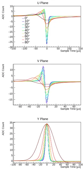
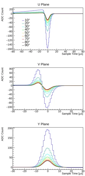
wire direction. It simply scales the charge deposition within one wire pitch by 1/(cosθxz·sinθy). As an example, figure 9 and figure10 demonstrate the TPC signal topology-dependency on θxz andθy. Note that the discussions above are related to the individual coordinates and angles for each wire plane. One track in the detector coordinate has different angles with respect to each wire plane’s coordinate.
Compared to the collection plane signals, the induction plane signals can be much smaller due to the cancellation of the various bipolar signals from all nearby elements of an extended event topology. In particular, for a track traveling in a direction close to normal to the wire planes (commonly referred to as aprolonged track), its induction plane signals will have low amplitude
and a long duration in time (figure9). This amplitude can be comparable to noise levels. Having the lowest achievable inherent electronics noise [27], avoiding excess noise sources, and applying proper signal processing are crucial to resolve the induction plane signals. Recovering these signals enables new opportunities to take full advantage of the LArTPC’s capability and reduce its residual ambiguities in later reconstruction. In order to minimize the inherent electronics noise, MicroBooNE uses a custom designed complementary metal-oxide-semiconductor (CMOS) analog front-end application-specific integrated circuit (ASIC) [28] operating at cryogenic temperatures inside the liquid argon. The close proximity of the preamplifier to the sense wire minimizes the input capacitance. The low temperature of LAr further reduces the electronics noise of the ASIC. The residual equivalent noise charge (ENC) after the software noise filtering varies with wire length and is found to be around 400 electrons for the longest wires (4.7 m) in MicroBooNE. This noise level is significantly lower than previous experiments utilizing warm front-end electronics. More details can be found in [27].
3 Reconstruction of drifted electron distribution
y’
z’
z (beam direction) y (vertical up)
x(x’) (drifting field direction)
Collection wire plane Induction wire plane
y(y’) wire direction z(z’) wire pitch direction
(a) Coordinates for collection and induction planes. They0(z0) axis is rotated by 60◦around the xaxis from the y (z) axis. The illustrated induction plane’s coordinate is consistent with the V plane’s and the U plane’s is with a rotation in the opposite direction.
x(drifting field direction) y(wire direction)
z(wire pitch direction) theta_xz
theta_y
𝜽
𝒚
𝜽
𝒙𝒛
(b) Definition of two angles,θxz andθy.
Figure 8: Geometric coordinates and angles for topology description.
3.1 Signal extraction principles
s] µ Sample Time [ 150
− −100 −50 0 50 100 150
ADC Count
30 −
25 −
20 −
15 −
10 −
5 −
0 5 10
° 0
° 10
° 20
° 30
° 40
° 50
° 60
° 70
° 80
U Plane
s] µ Sample Time [ 60
− −40 −20 0 20 40 60
ADC Count
15 −
10 −
5 −
0 5 10
V Plane
s] µ Sample Time [ 100
− −80 −60 −40 −20 0 20 40 60 80 100
ADC Count
0 5 10 15 20 25 30 35
[image:18.595.149.438.88.673.2]Y Plane
Figure 9: Simulated baseline-subtracted MicroBooNE TPC signals for a 1 meter long MIP track (≈4400 ionization electrons per mm) traveling perpendicular to each wire plane orientation (θy = 90◦) withθ
s] µ Sample Time [ 80
− −60 −40 −20 0 20 40 60 80
ADC Count 160 − 140 − 120 − 100 − 80 − 60 − 40 − 20 − 0 20 ° 10 ° 20 ° 30 ° 40 ° 50 ° 60 ° 70 ° 80 ° 90 U Plane s] µ Sample Time [ 30
− −20 −10 0 10 20 30
ADC Count 100 − 80 − 60 − 40 − 20 − 0 20 40 60 80 V Plane s] µ Sample Time [ 30
− −20 −10 0 10 20 30
[image:19.595.152.437.83.674.2]ADC Count 0 50 100 150 200 Y Plane
Figure 10: Simulated baseline-subtracted MicroBooNE TPC signals for a 1 meter long MIP track (≈4400 ionization electrons per mm), isochronous (θxz = 0◦) withθ
3.1.1 Deconvolution and software filters
The principal method to extract charge is deconvolution. This procedure in its one-dimensional (1D) form has been used in the data analysis of previous liquid argon experiments [29,30]. This technique has the advantages of being robust and fast. It is an essential step in the overall drifted-charge profiling process.
Deconvolution is a mathematical technique to extract theoriginal signalS(t)from themeasured signal M(t0). The measured signal is modeled as a convolution integral over the original signal S(t) and a given detector response functionR(t,t0), which gives the instantaneous portion of the measured signal at some timet0due to an element of original signal at timet:
M(t0)=
∫ ∞
−∞
R(t,t0) ·S(t)dt. (3.1)
If the detector response function is time-invariant, then R(t,t0) ≡ R(t0−t) and we can solve the above equation by performing a Fourier transformation, yielding M(ω)= R(ω) ·S(ω), whereωis in units of angular frequency. We can derive the signal in the frequency domain by taking the ratio of the measured signal and the given response function:
S(ω)= M(ω)
R(ω). (3.2)
In principle, the original signal in the time domain S(t) can then be obtained by applying the inverse Fourier transformation from the frequency domain S(ω). However in practice, there are two intermixed complicating effects. First, the measured signal M(t0) contains an additional contribution from various electronics noise sources [27]. Second, in realistic detectors, the response function R decreases substantially at high frequency (large ω). These two factors lead to high-frequency components of the noise spectrum being artificially amplified through equation3.2. If left unchecked, the derived signalS(ω) would be completely overwhelmed by noise. To address this issue, afilter functionF(ω)is introduced, yielding
S(ω)= M(ω)
R(ω) ·F(ω). (3.3)
Its purpose is to attenuate the problematic high frequency noise. The addition of the filter function F can be considered as a replacement of the response function R. In essence, the deconvolution replaces the real field and electronics response function with an effective software filter response function. The advantage of this procedure is most pronounced on the induction plane where the irregular bipolar field response function is replaced by a regular unipolar response function through the inclusion of the software filter.
A common choice of software filter is the Wiener filter3[32], which is based on the expected signalS2(ω)and noiseN2(ω)frequency spectra:
F(ω)= R2(ω)S2(ω) R2(ω)S2(ω)+N2(ω)
. (3.4)
With this construction, the Wiener filter is expected to achieve the best signal to noise ratio with minimal mean square error (the sum of the variance and the squared bias) of the deconvolved distribution. However, naively applying the Wiener filter to TPC signal processing is problematic for three reasons. Firstly, as described in section 2.3, the TPC signal S(ω) varies substantially depending on the exact nature of the event topology. The electronics noise spectrum is also a function of the duration of the time window over which it is observed. A longer time window allows for observation of more low frequency noise components. Therefore, it is impractical to achieve a universal Wiener filter yielding the best signal-to-noise ratio for all signals of varying time windows. Secondly, given the definition of the Wiener filter in equation3.4, we haveF(ω=0)< 1. Considering the addition of the filter as a replacement of the response functionR(t0−t), we can see that the Wiener filter does not conserve the total number of ionization electrons. Thirdly, as shown in equation 3.3, the filter acts as a replaced response function and smears the extracted ionization electron distribution along the drift time dimension. Since the drift time is equivalent to the drift distance, a filter that can alter the charge distribution in an extended (non-local) time range instead of in a short (local) one is undesirable. For induction wire planes, none of the ionization electrons are expected to be collected, which leads to a bipolar signal in the time domain and a low-frequency suppressed signal in the frequency domain. A direct construction of the Wiener filter with this low-frequency suppression would lead to a non-local charge smearing. To overcome these shortcomings associated with the Wiener filter, we use a Wiener-inspired filter. Details are elaborated upon in section3.2.2.
3.1.2 2D deconvolution
As described in section2, the induced current on the sense wire receives contributions not only from ionization charge passing by the sense wire, but also from ionization charge drifting in nearby wire regions. Naturally, the contribution of charge farther from the target sense wire is smaller. Ignoring the variation of the strength of the field response within one wire region, equation (3.1) can be expanded to
Mi(t0)=
∫ ∞
−∞
(...+R1(t0−t) ·Si−1(t)+R0(t0−t) ·Si(t)+R1(t0−t) ·Si+1(t)+...) ·dt, (3.5)
where Mi represents the measured signal from wirei. Si−1, Si, andSi+1represent the real signal inside the boundaries of wire i and its adjacent neighbors. R0 represents an average response function for an ionization charge passing through the wire region of interest. The average is taken over all possible drift paths through the wire region. Similarly,R1represents the average response function for an ionization charge drifting past in the next adjacent wire region. One can expand this definition ton number of neighbors by introducing terms up to Rn. Equation (3.5) assumes translational invariance in the response function (i.e. theRdoes not depend on the actual location of the wire). In section4.2.5, we will discuss the impact of ignoring position dependence of the field response at small scales within the wire region of interest.
If we then apply a Fourier transform on both sides of equation (3.5), we have:
which can be written in matrix notation as: © «
M1(ω) M2(ω)
...
Mn−1(ω) Mn(ω)
ª ® ® ® ® ® ® ® ¬ = © «
R0(ω) R1(ω) . . . Rn−2(ω) Rn−1(ω) R1(ω) R0(ω) . . . Rn−3(ω) Rn−2(ω)
... ... . . . ... ...
Rn−2(ω) Rn−3(ω) . . . R0(ω) R1(ω) Rn−1(ω) Rn−2(ω) . . . R1(ω) R0(ω)
ª ® ® ® ® ® ® ® ¬ · © «
S1(ω) S2(ω)
...
Sn−1(ω) Sn(ω)
ª ® ® ® ® ® ® ® ¬ (3.7)
Now, if we assume that we know all response functions (i.e. the matrixR), the problem converts into deducing the vectorS from the measured signalM by an inversion of matrixR, provided that the wires of interest are distant from the wire plane edges, the matrixRis symmetric and Toeplitz4, and the inverse problem can be solved using discrete-space Fourier transformation techniques as discussed in section3.1.1, onMi(ω), Si(ω), andRi(ω). Therefore, instead of 1D a deconvolution involving only the time dimension, a two-dimensional (2D) deconvolution involving both time and wire dimensions is performed to recover the ionization electron distribution. An additional Wiener-inspired filter is applied to the wire dimension deconvolution in analogy to that of the time domain deconvolution. These software filters will be discussed in section3.2.2.
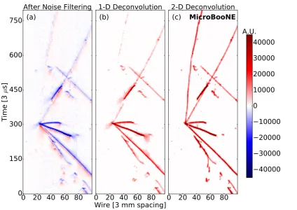
An example comparison of the 1D and 2D deconvolution results in a data event can be seen in figure11, demonstrating the charge recovery using the 2D deconvolution approach in contrast to the 1D method. Figure11highlights the signal dependence on topology and long range induction. An evaluation of 2D deconvolution signal processing performance given the topological dependence of the signal and the long range induction inherent to the signal is considered in section4.
3.1.3 Region of interest (ROI)
The 2D deconvolution procedure described in section3.1.2provides a robust and computationally-efficient method to extract the distribution of ionization electrons. While successful for the collection plane the procedure is still not optimal for the induction planes due to the bipolar nature of the measured induction plane signals. In order to illustrate this point, the average response functions on the closest wire for a point-like ionization charge is shown in figure12. The average response function includes both the average field response (averaged over all possible electron drift paths within the wire region as simulated by Garfield without diffusion) and the electronics response (2 µs peaking time). The normalization of the overall response function is chosen so that the integral of the collection plane response function is unity, corresponding to a single electron. Figure12bshows the frequency components of the average response functions for the three wire planes. All responses have suppressions at high frequency, where the filter is required to stabilize the deconvolved results (e.g. equation3.3). Compared to the collection wire response, the induction wire responses exhibit suppressions at low frequency. In particular, at zero frequency, the frequency components are equivalent to the integral of the response function over time and should be close to zero as indicated by equation2.4.
Similar to the situation at high frequencies, the suppression of the induction responses at low frequencies is problematic for the proposed deconvolution procedure. As shown in [27],
4A Toeplitz matrix is one for which each diagonal descending from left to right has all elements equal. Multiplication
0 20 40 60 80
0
150
300
450
600
750
Tim
e [
3
µ
s]
(a)
After Noise Filtering
0 20 40 60 80
Wire [3 mm spacing]
(b)
1-D Deconvolution
0 20 40 60 80
(c)
MicroBooNE
2-D Deconvolution
[image:23.595.85.510.86.386.2]40000
30000
20000
10000
0
10000
20000
30000
40000
A.U.
Figure 11: A neutrino candidate from MicroBooNE data (event 41075, run 3493) measured on the U plane. (a) Raw waveform after noise filtering in units of average baseline subtracted ADC scaled by 250 per 3 µs. (b) Charge spectrum in units of electrons per 3 µs after signal processing with 1D deconvolution. (c) Charge spectrum in units of electrons per 3 µs after signal processing with 2D deconvolution.
the measured signal contains electronics noise, which is not necessarily as suppressed at low frequencies. Therefore, following equation (3.3), the low frequency noise will be amplified in the deconvolution process. The amplification of low frequency noise can be seen clearly in figure18a. Left unmitigated, the amplification of low frequency noise would lead to an unacceptable uncertainty in the charge estimation.
In principle, the amplification of the low-frequency noise through the deconvolution process can be suppressed through the application of low-frequency (high-pass) filters similar to the filters suppressing high-frequency (low-pass) noise. However, as explained in section3.1.1, applying such a low-frequency filter would lead to an alteration of the charge distribution in extended (non-local) time ranges, which is not desirable. Instead we turn to the technique of selecting a signal region of interest (ROI) in the time domain.
s] µ Time [ 50
− −40 −30 −20 −10 0 10
s [e-]
µ
Integrated charge per 0.5
0.05 −
0 0.05 0.1 0.15
Closest Wire for an Electron
U plane
V plane
Y plane
(a) Average response in time domain.
Frequency [MHz] 0 0.1 0.2 0.3 0.4 0.5 0.6 0.7 0.8 0.9 1
Magnitude
0 0.2 0.4 0.6 0.8 1
(b) Average response in frequency domain.
Figure 12: Examples of simulated average response functions for induction (black and red) and collection (blue) wires in the time (a) and frequency (b) domains.
limits the low frequency noise. To illustrate this point, we consider a time window withNsamples. MicroBooNE samples at intervals of 0.5 µs and the highest frequency that can be resolved is the Nyquist frequency of 1 MHz. After a discrete Fourier transform, the bin above the first bin (zero frequency) starts at 1 MHzN/2 . The noise in the zero-frequency bin represents a baseline shift after the ROI is transformed back into the time domain. Therefore, once we identify the signal region and create a ROI just big enough to cover the signal, we can naturally suppress the low-frequency noise at the cost of having to correct for the baseline shift. This correction is performed through a linear interpolation of the two baselines, determined by samples at the start and end of the ROI window in the time domain.
3.2 Method
In this section, we describe the inputs and the detailed algorithms to extract the ionization charge spectrum from the digitized TPC wire plane signals, based on the principles described above. The algorithm is implemented and available at [33].
In general, the full chain contains four major steps:
• Noise filtering:
Apply specific noise filters to remove possible excess noise apart from the inherent electronics noise. The results of this step have been previously reported in [27].
• 2D deconvolution:
ADC waveforms A given wire plane;All channels
Excess Noise filtering
2D deconvolution
Filter in wire dimension Two types of filters in time dimension
Apply HF-cut Gaussian filter
Notation
HF(LF): high(low) frequency RMS: noise root mean square
Apply HF-cut Wiener filter
Induction plane No
Apply loose LF-cut filter
Yes
RMS calculation
Apply tight LF-cut filter
RMS calculation
Initial ‘loose ROIs’
Initial ‘tight ROIs’
Connectivity Extension or creation
Intermediate ROIs
Clean ROIs
Break ROIs Shrink ROIs
Refinement of ROIs
Induction
Final ROIs
Apply ROIs
Deconvolved charge
Yes
Baseline subtraction
[image:25.595.101.500.88.307.2]No
Figure 13: A flow chart of the full chain of signal processing. See text for explanation.
applied to maximize the signal-to-noise ratio with better time resolution and a Gaussian filter is applied to achieve a non-distorted charge spectrum except for a Gaussian smearing. Details will be explained in section3.2.2.
• ROI finding and refining:
Perform ROI finding with the deconvolved charge distribution after the Wiener-inspired filter. The principle of these algorithms will be explained in section3.2.3and 3.2.4. In short, loose and tight high-pass filters are combined to optimize the purity and efficiency of ROI finding. • ROI application:
Apply the identified ROI window to the deconvolved charge distribution after the Gaussian filter and extract the ionization charge, with a linear baseline subtraction for the induction planes based on the start/end bins of the ROI window.
A flow chart of the full chain of the aforementioned signal processing can be seen in figure13.
3.2.1 Position-averaged response functions
Since the signal in a readout wire is recorded without any prior knowledge of the transverse position distribution of electrons within a wire region, the average response functions are used in the 2D deconvolution as discussed in section 3.1.2. The average response function for a single electron within a particular wire region is obtained through the following summation:
Ri =
0.5×Ri0.0mm+Ri0.3mm+Ri0.6mm+R0i.9mm+Ri1.2mm+0.5×Ri1.5mm
5 , (3.8)
explained in section4.2.5. These average responses for 21 wires (the central wire± 10 wires on both sides) are shown in figure 14. The left panel shows the response function in 2D with the “Log10” scale. The X-axis represents the wire number. The Y-axis represents the drift time with 1 tick of 0.5 µs in each bin. The normalization is the same as that in figure4. The right panel shows the average response function in a linear scale for the first five wires. For the V and Y wire planes, the strength of the response function drops quickly for wires further away from the central wire (i.e. negligible beyond±4 wires). For the U induction wire plane, the strength of the response function is still sizable at±4 wires. This is due to the fact that the U induction wire plane is the first wire plane facing the active TPC volume without any shielding.
3.2.2 Software filters
In this section, we describe the derivation of the software filters used in the signal processing. As mentioned in section3.1.1, the chosen Wiener-inspired filter is based on the Wiener filter in equation3.4constructed from simulation. The time window is chosen to be 100µs which generally performs well in a variety of cases with proper additional smearing of the signal. The signal is chosen to be an isochronous MIP track traveling perpendicular to the wire orientation. The total number of ionization electrons is assumed to be 1.6×10⁴per wire pitch. The RMS of the spread in the drift time due to diffusion is taken to be 1 mm, corresponding to the average drift distance in the MicroBooNE detector. The gain and peaking time are 14 mV/fC and 2µs, which is the same as the nominal running condition [27]. The electronic noise is simulated in an analytic way, as will be described in section4.2.6. The results following equation (3.4) were then fitted with the following functional form in order to exclude low-frequency suppressions presented in the original Wiener filters:
F(ω)= c·e−12·(ωa) b
, (3.9)
where a, b, c are free parameters to be determined by the fit. This functional form of the filter guarantees that the corresponding smearing function (filter) in the time domain is local. Given the fit, the filter is chosen to be
F(ω)=
(
e−12·(ωa) b
ω >0
0 ω=0, (3.10)
withaandbbeing the same parameters as in equation3.9withcremoved. The modification of the filter takes into account the following considerations:
• The filter is explicitly zero atω=0 in order to remove any DC component in the deconvolved signal. This removes information about the baseline. A new baseline is calculated and restored for the waveform after deconvolution.
• The above functional form of the filter leads to
lim
ω→0F(ω)=1. (3.11)
Wire Number 10
− −5 0 5 10
s] µ Time [ 60 − 50 −40 − 30 −20 − 10 − 0 10 20 30 40 ''Log 10'' 3 − 2 − 1 − 0 1 2 3 U Plane Wire Number 10
− −5 0 5 10
s] µ Time [ 60 − 50 −40 −30 −20 −10 − 0 10 20 30 40 ''Log 10'' 3 − 2 − 1 − 0 1 2 3 V Plane Wire Number 10
− −5 0 5 10
s] µ Time [ 60 −50 −40 − 30 −20 − 10 − 0 10 20 30 40 ''Log 10'' 3 − 2 − 1 − 0 1 2 3 4 Y Plane
(a) Wire number versus time in “Log10” scale.
s]
µ
Time [ 60
− −40 −20 0 20 40
s] µ /0.5 -Current [e 0.06 − 0.04 − 0.02 − 0 0.02 0.04 0.06 Central Wire 1 Wire ± 2 Wire ± 3 Wire ± 4 Wire ± U Plane s] µ Time [ 60
− −40 −20 0 20 40
s] µ /0.5 -Current [e 0.06 − 0.04 − 0.02 − 0 0.02 0.04 0.06 V Plane s] µ Time [ 60
− −40 −20 0 20 40
s] µ /0.5 -Current [e 0.05 − 0 0.05 0.1 0.15 Y Plane
[image:27.595.87.492.87.495.2](b) Response functions for each of the first five wires.
Figure 14: The position-averaged response functions after convolving the field response function and an electronics response function at 2 µs peaking time in “Log 10” scale (a) and linear scale for the first 5 wires (b).
Figure15shows the three Wiener-inspired filters and a Gaussian filter,
F(ω)=
(
e−12·(ωa)
2
ω >0
0 ω=0, (3.12)
s] µ Time [ 20
− −15 −10 −5 0 5 10 15 20
s
µ
Magnitude/0.5
0.05 −
0 0.05 0.1 0.15
0.2 U planeV plane
Y plane Gaus
(a) Filters in the time domain.
Frequency [MHz] 0 0.1 0.2 0.3 0.4 0.5 0.6 0.7 0.8 0.9 1
Magnitude
0 0.2 0.4 0.6 0.8 1
(b) Filters in the frequency domain.
Figure 15: Wiener-inspired (dashed line) and Gaussian (solid line) software filters are shown in (a) the time domain and (b) the frequency domain for each of the three wire planes. In the time domain, we commonly refer to the filter function as the smearing function. With the chosen functional forms, the local behavior of the filters is apparent from their shapes.
reconstruction.
In 2D deconvolution, a similar filter in the wire dimension is constructed using the Gaussian form
F(ωw)= e−12·(ωaw)
2
(3.13) where the “frequency”,ωw, is the Fourier transform over the wire number instead of time. Figure16
shows the filters in the wire domain. Different parameters are chosen for induction and collection wire planes.
3.2.3 Identification of signal ROIs
As shown in figure18a, the direct application of the deconvolution procedure significantly amplifies the low-frequency noise for the induction wire planes. In order to identify the signal regions of interest (signal ROIs or ROIs for short), additional low-frequency filters with a functional form
FLF(ω)=1−e(ωa)
2
, (3.14)
are applied to the deconvolved charge distribution for the induction wire planes to search for ROIs. These low-frequency filters are not used for the collection wire plane signal.
Wire Number 10
− −8 −6 −4 −2 0 2 4 6 8 10
Magnitude
0 0.2 0.4 0.6 0.8 1
Induction plane
Collection plane
(a) Wire filters in the wire number domain.
Frequency
0 0.1 0.2 0.3 0.4 0.5
Magnitude
0.5 0.6 0.7 0.8 0.9 1
[image:29.595.85.493.112.303.2](b) Wire filters in the “frequency” domain.
Figure 16: Filters using a Gaussian form are applied for the wire dimension shown in both the wire number (a) and “frequency” (b) domains. Different parameters are chosen for induction and collection wire planes.
s] µ Time [ 30
− −20 −10 0 10 20 30
s
µ
Magnitude/0.5
0 0.2 0.4 0.6 0.8 1
Loose
Tight
Low-f filters
(a) Low-frequency filters in the time domain.
Frequency [MHz] 0 0.02 0.04 0.06 0.08 0.1
Magnitude
0 0.2 0.4 0.6 0.8 1
(b) Low-frequency filters in the frequency do-main.
[image:29.595.86.496.434.620.2]s]
µ
Tick [0.5 0 2000 4000 6000 8000
s
µ
Electrons/0.5
2000 −
0 2000 4000
6000 MicroBooNE
(a) Without low-frequency filter.
s]
µ
Tick [0.5 0 2000 4000 6000 8000
s
µ
Electrons/0.5
2000 −
0 2000 4000
6000 MicroBooNE
(b) With tight low-frequency filter.
s]
µ
Tick [0.5 0 2000 4000 6000 8000
s
µ
Electrons/0.5
2000 −
0 2000 4000 6000
MicroBooNE
[image:30.595.106.487.81.449.2](c) With loose low-frequency filter.
Figure 18: Comparison of the deconvolved signal on the U induction plane (a) without the low-frequency filter, (b) with the tight low-low-frequency filter, and (c) with the loose low-low-frequency filter.
Figure18shows the impact of these low-frequency filters. Without the filter, the low-frequency noise totally overwhelms the signal (figure 18a). After applying the tight low-frequency filter (figure18b), the signal-to-noise ratio improves for short (in time) signals. However, the long signal at around 7000 time ticks is removed by the tight low-frequency filter. It is recovered by the loose low-frequency filter (figure18c).
ROIs are then extracted from these deconvolved signals. For the induction wire planes, there are two types of ROIs: tight and loose ROIs, which are extracted from the deconvolved signal after applying tight and loose low-frequency filters, respectively. The goal of the tight ROIs is to achieve high purity in terms of containing real signal. However, it is expected that tight ROIs have a low efficiency, in particular for long (in time) signals. On the other hand, the goal of the loose ROIs is to achieve high efficiency in terms of containing real signal. The trade-off is that we expect the purity of the loose ROIs to be lower. ROIs are then extracted by searching for signal above noise. Each ROI is then extended in time to cover the signal tails. For (ROIs) tight ROIs in the (collection) induction plane, additional ROIs are created by examining the connectivity of the existing ones. Each of the loose ROIs is then compared with the tight ROIs on the same wire. If one loose ROI overlaps with a tight ROI, the loose ROI is extended to ensure the tight ROI is contained. If a tight ROI is not contained by a loose ROI, a new loose ROI with the exact range of the tight ROI is created. The operations above ensure that each tight ROI is contained by a loose ROI. Figure19
shows the impact of including tight and loose ROIs for the induction plane signal processing.
3.2.4 Refinement of ROIs
As explained previously, the loose ROIs for the induction wire plane are expected to have a high efficiency in containing the real signal, but low purity. Therefore, an additional refining procedure using connectivity information is applied to exclude fake ROIs.
The basic components of the ROI refinement include:
• Clean ROIs:
The motivation of this step is to remove fake ROIs—ROIs containing no signal. In particular, each loose and tight ROI is examined to ensure that part of the bin content inside the ROI is above a predefined threshold. ROIs failing this examination are removed. Loose ROIs are clustered according to connectivity information. For each loose ROI cluster, if none of its loose ROIs contain one or more tight ROIs, the cluster is removed entirely.
• Break ROIs:
The motivation of this step is to separate a loose ROI into a few small ROIs. Sometimes a few separated tracks (e.g. near the neutrino interaction vertex) can be quite close to each other along the drift time direction. Often a single loose ROI would be created to contain these tracks given the presence of low-frequency noise. Therefore, a special algorithm is needed to identify this scenario and separate the ROIs. In particular, each loose ROI is examined to search for multiple independent peaks. If found, the loose ROI is separated into several loose ROIs. Figure20shows the impact of the “break ROIs” step.
• Shrink ROIs:
Channel ID
1100 1200 1300 1400 1500
TIme Ticks
5500 6000 6500 7000 7500 8000
MicroBooNE
(a) Deconvolved signal with “loose and tight ROIs”.
Channel ID
1100 1200 1300 1400 1500
TIme Ticks
5500 6000 6500 7000 7500 8000
MicroBooNE
(b) Deconvolved signal with “tight ROIs”.
Time Ticks 6600 6800 7000 7200
ADC Counts/1 tick
-100 -50 0 50
Raw Waveform With Only Tight ROIs With Loose and Tight ROIs
MicroBooNE
Electrons/6 ticks (x 500)
-100 -50 0 50
[image:32.595.203.396.386.546.2](c) Waveform comparison for the channel marked with a red line in (a) and (b).
Channel ID
1100 1200 1300 1400 1500
TIme Ticks
5500 6000 6500 7000 7500 8000
MicroBooNE
(a) Deconvolved signal with “break ROIs”.
Channel ID
1100 1200 1300 1400 1500
TIme Ticks
5500 6000 6500 7000 7500 8000
MicroBooNE
(b) Deconvolved signal without “break ROIs”.
Time Ticks 5400 5500 5600 5700 5800 5900
ADC Counts/1 tick
-40 -20 0 20 40
Raw Waveform With Break ROIs Without Break ROIs
MicroBooNE
Electrons/6 ticks (x 500)
-40 -20 0 20 40
[image:33.595.208.391.307.463.2](c) Waveform comparison for the channel marked with a red line in (a) and (b).
Figure 20: The same neutrino candidate from figure19is shown in an event display with (a) and without (b) “break ROIs”. In (c), the raw baseline-subtracted waveform (black) and the deconvolved signal with (dotted red) and without (dashed red) “break ROIs” are presented.
The overall ROI refinement takes an iterative approach by applying the above steps in sequence. The final remaining ROIs are then applied to the deconvolved signal without the low-frequency filter. A linear correction to the baseline is applied so that the bin content of the ROI boundaries are exactly zero.
4 Evaluating TPC signal processing with simulation
Channel ID
1100 1200 1300 1400 1500
TIme Ticks
5500 6000 6500 7000 7500 8000
MicroBooNE
(a) Deconvolved signal with “shrink ROIs”.
Channel ID
1100 1200 1300 1400 1500
TIme Ticks
5500 6000 6500 7000 7500 8000
MicroBooNE
(b) Deconvolved signal without “shrink ROIs”.
Time Ticks
6100 6200 6300 6400 6500
ADC Counts/1 tick
-20 0 20 40
Raw Waveform With Shrink ROIs Without Shrink ROIs
MicroBooNE
Electrons/6 ticks (x 500)
-20 0 20 40
[image:34.595.207.392.308.462.2](c) Waveform comparison for channel marked with red line in (a) and (b).
Figure 21: The same neutrino candidate from figure 19 is shown in an event display with (a) and without (b) “shrink ROIs”. In (c), the raw baseline-subtracteed waveform (black) and the deconvolved signal with (dotted red) and without (dashed red) “shrink ROIs” are presented.
is demonstrated including measures of reconstructed charge resolution, bias, and efficiency. The simulation itself is validated against MicroBooNE detector data in [19].
4.1 Key simulation improvements
Evaluation of the signal processing relies, in part, on an improved signal and noise simulation. The signal simulation has two key improvements compared to prior implementations.
![Figure 1: Diagram illustrating the signal formation in a LArTPC with three wire planes [12]](https://thumb-us.123doks.com/thumbv2/123dok_us/9315903.433324/5.595.105.520.129.428/figure-diagram-illustrating-signal-formation-lartpc-wire-planes.webp)