UG04221 000B 4221 Condor VME Ethernet Users Guide Jul94 pdf
124
0
0
Full text
(2)
(3) Copyright Notice Copyright 1993, 1994 by Interphase Corporation All rights reserved No part of this publication may be stored in a retrieval system, transmitted, or reproduced in any way, including, but not limited to photocopy, photograph, electronic, or mechanical, without prior written permission of:. Interphase Corporation 13800 Senlac Dallas, Texas 75234 Phone: (214) 919-9000 FAX: (214) 919-9200. Disclaimer Information in this user document supercedes any preliminary specification, data sheets, and/or any other documents that may have been made available. Every effort has been made to supply accurate and complete information. However, Interphase Corporation assumes no responsibility or liability for its use. In addition, Interphase Corporation reserves the right to make product improvement without prior notice. Such improvements may include, but not limited to, command codes and error codes..
(4) For Assistance To place an order for an Interphase product, call: Sales Support: (214) 919-9000. For assistance using this, or any other Interphase product, call: Customer Service: (214) 919-9000 United Kingdom: +44-869-321222. To send in a board for repair or upgrade, call: RMA Coordinator: (214) 919-9000. Trademark Acknowledgments All terms used in this manual that are known to be trademarks or service marks are listed below. In addition, terms suspected of being trademarks have been appropriately capitalized. Use of a term in this manual should not be regarded as affecting the validity of any trademark or service mark. •. Interphase is a registered trademark of Interphase Corporation.. •. Virtual Buffer ArchitectureSM, BUSpacket InterfaceSM, and CacheFlowSM are service marks of Interphase Corporation.. •. UNIX® is a registered trademark of AT&T Bell Laboratories.. •. IBM® is a registered trademark of International Business Machines.. •. 80486® 82503®, and 82596A® are registered trademarks/product marks of Intel.. •. MC68EC030® and MC68040® are registered trademarks/product marks of Motorola..
(5) TABLE OF CONTENTS CHAPTER 1 INTRODUCTION . . . . . . . . . . . . . . . . . . . . . . . . . . . . . . . . . . . . . . . . . . . . . . . . . . . . . . . . . . . . . . . . . . . . . . . . . Intended Audience . . . . . . . . . . . . . . . . . . . . . . . . . . . . . . . . . . . . . . . . . . . . . . . . . . . . . . . . . . . . . . . . . . . . . . . . . Scope Of Manual . . . . . . . . . . . . . . . . . . . . . . . . . . . . . . . . . . . . . . . . . . . . . . . . . . . . . . . . . . . . . . . . . . . . . . . . . . References . . . . . . . . . . . . . . . . . . . . . . . . . . . . . . . . . . . . . . . . . . . . . . . . . . . . . . . . . . . . . . . . . . . . . . . . . . . . . . . Conventions . . . . . . . . . . . . . . . . . . . . . . . . . . . . . . . . . . . . . . . . . . . . . . . . . . . . . . . . . . . . . . . . . . . . . . . . . . . . . . General Description . . . . . . . . . . . . . . . . . . . . . . . . . . . . . . . . . . . . . . . . . . . . . . . . . . . . . . . . . . . . . . . . . . . . . . . . Features . . . . . . . . . . . . . . . . . . . . . . . . . . . . . . . . . . . . . . . . . . . . . . . . . . . . . . . . . . . . . . . . . . . . . . . . . . . . . . . . . Options . . . . . . . . . . . . . . . . . . . . . . . . . . . . . . . . . . . . . . . . . . . . . . . . . . . . . . . . . . . . . . . . . . . . . . . . . . . . . . . . . . Physical Description . . . . . . . . . . . . . . . . . . . . . . . . . . . . . . . . . . . . . . . . . . . . . . . . . . . . . . . . . . . . . . . . . . . . . . . Functional Description . . . . . . . . . . . . . . . . . . . . . . . . . . . . . . . . . . . . . . . . . . . . . . . . . . . . . . . . . . . . . . . . . . . . . . Ethernet Front End Channel (FEC) . . . . . . . . . . . . . . . . . . . . . . . . . . . . . . . . . . . . . . . . . . . . . . . . . . . . . . . . . . . . VMEbus Master Interface . . . . . . . . . . . . . . . . . . . . . . . . . . . . . . . . . . . . . . . . . . . . . . . . . . . . . . . . . . . . . . . . . . . DMA Engine . . . . . . . . . . . . . . . . . . . . . . . . . . . . . . . . . . . . . . . . . . . . . . . . . . . . . . . . . . . . . . . . . . . . . . VMEbus Drivers And Receivers . . . . . . . . . . . . . . . . . . . . . . . . . . . . . . . . . . . . . . . . . . . . . . . . . . . . . . . Local Bus . . . . . . . . . . . . . . . . . . . . . . . . . . . . . . . . . . . . . . . . . . . . . . . . . . . . . . . . . . . . . . . . . . . . . . . . . . . . . . . . VMEbus Short I/O Interface . . . . . . . . . . . . . . . . . . . . . . . . . . . . . . . . . . . . . . . . . . . . . . . . . . . . . . . . . . . . . . . . . CPU Core . . . . . . . . . . . . . . . . . . . . . . . . . . . . . . . . . . . . . . . . . . . . . . . . . . . . . . . . . . . . . . . . . . . . . . . . . . . . . . . . CPU/LBUS Interface . . . . . . . . . . . . . . . . . . . . . . . . . . . . . . . . . . . . . . . . . . . . . . . . . . . . . . . . . . . . . . . . . . . . . . .. 1 1 1 1 2 2 2 3 3 3 4 4 4 4 4 5 5 6. CHAPTER 2 HARDWARE INSTALLATION . . . . . . . . . . . . . . . . . . . . . . . . . . . . . . . . . . . . . . . . . . . . . . . . . . . . . . . . . . . . . 7 Overview . . . . . . . . . . . . . . . . . . . . . . . . . . . . . . . . . . . . . . . . . . . . . . . . . . . . . . . . . . . . . . . . . . . . . . . . . . . . . . . . 7 4221 Condor Hardware Installation Procedures . . . . . . . . . . . . . . . . . . . . . . . . . . . . . . . . . . . . . . . . . . . . . . . . . 14 Step 1. Visual Inspection . . . . . . . . . . . . . . . . . . . . . . . . . . . . . . . . . . . . . . . . . . . . . . . . . . . . . . . . . . . . 14 Step 2. Fuse And Diagnostic LEDs . . . . . . . . . . . . . . . . . . . . . . . . . . . . . . . . . . . . . . . . . . . . . . . . . . . . 14 Step 3. Set Onboard Motherboard Jumpers . . . . . . . . . . . . . . . . . . . . . . . . . . . . . . . . . . . . . . . . . . . . . 16 Step 4. Set Daughter Card Jumpers And Terminations. . . . . . . . . . . . . . . . . . . . . . . . . . . . . . . . . . . . . 47 Step 5. Power Off System . . . . . . . . . . . . . . . . . . . . . . . . . . . . . . . . . . . . . . . . . . . . . . . . . . . . . . . . . . . 51 Step 6. Cabling Procedure . . . . . . . . . . . . . . . . . . . . . . . . . . . . . . . . . . . . . . . . . . . . . . . . . . . . . . . . . . . 51 CHAPTER 3 MACSI HOST INTERFACE. . . . . . . . . . . . . . . . . . . . . . . . . . . . . . . . . . . . . . . . . . . . . . . . . . . . . . . . . . . . . . . . Introduction . . . . . . . . . . . . . . . . . . . . . . . . . . . . . . . . . . . . . . . . . . . . . . . . . . . . . . . . . . . . . . . . . . . . . . . . . . . . . Typographic Convention . . . . . . . . . . . . . . . . . . . . . . . . . . . . . . . . . . . . . . . . . . . . . . . . . . . . . . . . . . . . . . . . . . . Memory Address . . . . . . . . . . . . . . . . . . . . . . . . . . . . . . . . . . . . . . . . . . . . . . . . . . . . . . . . . . . . . . . . . . Field Offset . . . . . . . . . . . . . . . . . . . . . . . . . . . . . . . . . . . . . . . . . . . . . . . . . . . . . . . . . . . . . . . . . . . . . . Contiguous Data Allocation . . . . . . . . . . . . . . . . . . . . . . . . . . . . . . . . . . . . . . . . . . . . . . . . . . . . . . . . . System Interface. . . . . . . . . . . . . . . . . . . . . . . . . . . . . . . . . . . . . . . . . . . . . . . . . . . . . . . . . . . . . . . . . . . . . . . . . . MACSI Organization . . . . . . . . . . . . . . . . . . . . . . . . . . . . . . . . . . . . . . . . . . . . . . . . . . . . . . . . . . . . . . . . . . . . . . Master Control Status Block (MCSB) . . . . . . . . . . . . . . . . . . . . . . . . . . . . . . . . . . . . . . . . . . . . . . . . . . . . . . . . . Master Status Register (MSR) . . . . . . . . . . . . . . . . . . . . . . . . . . . . . . . . . . . . . . . . . . . . . . . . . . . . . . . . Master Control Register (MCR) . . . . . . . . . . . . . . . . . . . . . . . . . . . . . . . . . . . . . . . . . . . . . . . . . . . . . . Onboard Command Queue Entry. . . . . . . . . . . . . . . . . . . . . . . . . . . . . . . . . . . . . . . . . . . . . . . . . . . . . . . . . . . . . Queue Entry Control Register (QECR) . . . . . . . . . . . . . . . . . . . . . . . . . . . . . . . . . . . . . . . . . . . . . . . . . IOPB Address . . . . . . . . . . . . . . . . . . . . . . . . . . . . . . . . . . . . . . . . . . . . . . . . . . . . . . . . . . . . . . . . . . . . Command Tag . . . . . . . . . . . . . . . . . . . . . . . . . . . . . . . . . . . . . . . . . . . . . . . . . . . . . . . . . . . . . . . . . . . . Work Queue Number. . . . . . . . . . . . . . . . . . . . . . . . . . . . . . . . . . . . . . . . . . . . . . . . . . . . . . . . . . . . . . . Offboard Command Queue Entry . . . . . . . . . . . . . . . . . . . . . . . . . . . . . . . . . . . . . . . . . . . . . . . . . . . . . . . . . . . . Queue Entry Control Register (QECR) . . . . . . . . . . . . . . . . . . . . . . . . . . . . . . . . . . . . . . . . . . . . . . . . . DMA Transfer Control Word . . . . . . . . . . . . . . . . . . . . . . . . . . . . . . . . . . . . . . . . . . . . . . . . . . . . . . . . Host Address . . . . . . . . . . . . . . . . . . . . . . . . . . . . . . . . . . . . . . . . . . . . . . . . . . . . . . . . . . . . . . . . . . . . . Offboard Transfer Length . . . . . . . . . . . . . . . . . . . . . . . . . . . . . . . . . . . . . . . . . . . . . . . . . . . . . . . . . . . Work Queue Number. . . . . . . . . . . . . . . . . . . . . . . . . . . . . . . . . . . . . . . . . . . . . . . . . . . . . . . . . . . . . . . vi. 53 53 53 53 54 54 55 55 57 57 58 59 59 60 60 60 60 60 61 61 61 61.
(6) Command Response Block (CRB) . . . . . . . . . . . . . . . . . . . . . . . . . . . . . . . . . . . . . . . . . . . . . . . . . . . . . . . . . . . . 62 Command Response Status Word (CRSW) . . . . . . . . . . . . . . . . . . . . . . . . . . . . . . . . . . . . . . . . . . . . . . 62 Command Tag. . . . . . . . . . . . . . . . . . . . . . . . . . . . . . . . . . . . . . . . . . . . . . . . . . . . . . . . . . . . . . . . . . . . . 63 IOPB Length . . . . . . . . . . . . . . . . . . . . . . . . . . . . . . . . . . . . . . . . . . . . . . . . . . . . . . . . . . . . . . . . . . . . . . 63 Work Queue Number . . . . . . . . . . . . . . . . . . . . . . . . . . . . . . . . . . . . . . . . . . . . . . . . . . . . . . . . . . . . . . . 63 Multiple Completed Returned IOPB Structure . . . . . . . . . . . . . . . . . . . . . . . . . . . . . . . . . . . . . . . . . . . . . . . . . . . 64 Command Tag. . . . . . . . . . . . . . . . . . . . . . . . . . . . . . . . . . . . . . . . . . . . . . . . . . . . . . . . . . . . . . . . . . . . . 64 Port . . . . . . . . . . . . . . . . . . . . . . . . . . . . . . . . . . . . . . . . . . . . . . . . . . . . . . . . . . . . . . . . . . . . . . . . . . . . . 64 Work Queue Number . . . . . . . . . . . . . . . . . . . . . . . . . . . . . . . . . . . . . . . . . . . . . . . . . . . . . . . . . . . . . . . 64 Transfer Count . . . . . . . . . . . . . . . . . . . . . . . . . . . . . . . . . . . . . . . . . . . . . . . . . . . . . . . . . . . . . . . . . . . . 64 Configuration Status Block (CSB) . . . . . . . . . . . . . . . . . . . . . . . . . . . . . . . . . . . . . . . . . . . . . . . . . . . . . . . . . . . . 65 Product Code. . . . . . . . . . . . . . . . . . . . . . . . . . . . . . . . . . . . . . . . . . . . . . . . . . . . . . . . . . . . . . . . . . . . . . 65 Product Variation . . . . . . . . . . . . . . . . . . . . . . . . . . . . . . . . . . . . . . . . . . . . . . . . . . . . . . . . . . . . . . . . . . 65 Firmware Revision Level . . . . . . . . . . . . . . . . . . . . . . . . . . . . . . . . . . . . . . . . . . . . . . . . . . . . . . . . . . . . 66 Firmware Revision Date . . . . . . . . . . . . . . . . . . . . . . . . . . . . . . . . . . . . . . . . . . . . . . . . . . . . . . . . . . . . . 66 Ethernet MAC Addresses (Ports 0 - 3) . . . . . . . . . . . . . . . . . . . . . . . . . . . . . . . . . . . . . . . . . . . . . . . . . . 66 Controller Statistics Block . . . . . . . . . . . . . . . . . . . . . . . . . . . . . . . . . . . . . . . . . . . . . . . . . . . . . . . . . . . . . . . . . . 67 Transmit Commands Submitted . . . . . . . . . . . . . . . . . . . . . . . . . . . . . . . . . . . . . . . . . . . . . . . . . . . . . . . 68 Transmit DMA Completions . . . . . . . . . . . . . . . . . . . . . . . . . . . . . . . . . . . . . . . . . . . . . . . . . . . . . . . . . 68 Transmit 82596 Completions . . . . . . . . . . . . . . . . . . . . . . . . . . . . . . . . . . . . . . . . . . . . . . . . . . . . . . . . . 68 Successful Transmits . . . . . . . . . . . . . . . . . . . . . . . . . . . . . . . . . . . . . . . . . . . . . . . . . . . . . . . . . . . . . . . 68 Failed Transmits . . . . . . . . . . . . . . . . . . . . . . . . . . . . . . . . . . . . . . . . . . . . . . . . . . . . . . . . . . . . . . . . . . . 68 Transmit Completions Posted to Host . . . . . . . . . . . . . . . . . . . . . . . . . . . . . . . . . . . . . . . . . . . . . . . . . . 69 Receive Commands Submitted. . . . . . . . . . . . . . . . . . . . . . . . . . . . . . . . . . . . . . . . . . . . . . . . . . . . . . . . 69 Receives Dropped - No Pending Receive Command . . . . . . . . . . . . . . . . . . . . . . . . . . . . . . . . . . . . . . . 69 Receive 82596 Completions . . . . . . . . . . . . . . . . . . . . . . . . . . . . . . . . . . . . . . . . . . . . . . . . . . . . . . . . . . 69 Failed Receives . . . . . . . . . . . . . . . . . . . . . . . . . . . . . . . . . . . . . . . . . . . . . . . . . . . . . . . . . . . . . . . . . . . . 69 Receive DMA Completions . . . . . . . . . . . . . . . . . . . . . . . . . . . . . . . . . . . . . . . . . . . . . . . . . . . . . . . . . . 69 Receive Completions Posted to Host . . . . . . . . . . . . . . . . . . . . . . . . . . . . . . . . . . . . . . . . . . . . . . . . . . . 69 IO Parameter Blocks (IOPBs) . . . . . . . . . . . . . . . . . . . . . . . . . . . . . . . . . . . . . . . . . . . . . . . . . . . . . . . . . . . . . . . . 70 Common IOPB Structures. . . . . . . . . . . . . . . . . . . . . . . . . . . . . . . . . . . . . . . . . . . . . . . . . . . . . . . . . . . . . . . . . . . 70 Command Code . . . . . . . . . . . . . . . . . . . . . . . . . . . . . . . . . . . . . . . . . . . . . . . . . . . . . . . . . . . . . . . . . . . 71 Command Options . . . . . . . . . . . . . . . . . . . . . . . . . . . . . . . . . . . . . . . . . . . . . . . . . . . . . . . . . . . . . . . . . 71 Return Status. . . . . . . . . . . . . . . . . . . . . . . . . . . . . . . . . . . . . . . . . . . . . . . . . . . . . . . . . . . . . . . . . . . . . . 71 Normal Completion Level / Vector . . . . . . . . . . . . . . . . . . . . . . . . . . . . . . . . . . . . . . . . . . . . . . . . . . . . 71 Error Completion Level / Vector . . . . . . . . . . . . . . . . . . . . . . . . . . . . . . . . . . . . . . . . . . . . . . . . . . . . . . 71 DMA Transfer Control Word . . . . . . . . . . . . . . . . . . . . . . . . . . . . . . . . . . . . . . . . . . . . . . . . . . . . . . . . . 71 Initialize Controller . . . . . . . . . . . . . . . . . . . . . . . . . . . . . . . . . . . . . . . . . . . . . . . . . . . . . . . . . . . . . . . . . . . . . . . . 73 Command Code . . . . . . . . . . . . . . . . . . . . . . . . . . . . . . . . . . . . . . . . . . . . . . . . . . . . . . . . . . . . . . . . . . . 73 Controller Initialization Block Offset . . . . . . . . . . . . . . . . . . . . . . . . . . . . . . . . . . . . . . . . . . . . . . . . . . . 73 Controller Initialization Block (CIB) . . . . . . . . . . . . . . . . . . . . . . . . . . . . . . . . . . . . . . . . . . . . . . . . . . . . . . . . . . 74 Number of CQE Entries . . . . . . . . . . . . . . . . . . . . . . . . . . . . . . . . . . . . . . . . . . . . . . . . . . . . . . . . . . . . . 74 Special Network Options . . . . . . . . . . . . . . . . . . . . . . . . . . . . . . . . . . . . . . . . . . . . . . . . . . . . . . . . . . . . 75 Ethernet Physical Node Addresses . . . . . . . . . . . . . . . . . . . . . . . . . . . . . . . . . . . . . . . . . . . . . . . . . . . . . 75 Interrupt Levels and Vectors. . . . . . . . . . . . . . . . . . . . . . . . . . . . . . . . . . . . . . . . . . . . . . . . . . . . . . . . . . 75 DMA Burst Count. . . . . . . . . . . . . . . . . . . . . . . . . . . . . . . . . . . . . . . . . . . . . . . . . . . . . . . . . . . . . . . . . . 75 Offboard CRB DMA Transfer Control Word. . . . . . . . . . . . . . . . . . . . . . . . . . . . . . . . . . . . . . . . . . . . . 76 Offboard CRB host address . . . . . . . . . . . . . . . . . . . . . . . . . . . . . . . . . . . . . . . . . . . . . . . . . . . . . . . . . . 76 MAC Control/Status . . . . . . . . . . . . . . . . . . . . . . . . . . . . . . . . . . . . . . . . . . . . . . . . . . . . . . . . . . . . . . . . . . . . . . . 77 Command Code . . . . . . . . . . . . . . . . . . . . . . . . . . . . . . . . . . . . . . . . . . . . . . . . . . . . . . . . . . . . . . . . . . . 78 Command Options . . . . . . . . . . . . . . . . . . . . . . . . . . . . . . . . . . . . . . . . . . . . . . . . . . . . . . . . . . . . . . . . . 79 Return Status. . . . . . . . . . . . . . . . . . . . . . . . . . . . . . . . . . . . . . . . . . . . . . . . . . . . . . . . . . . . . . . . . . . . . . 80 Buffer address . . . . . . . . . . . . . . . . . . . . . . . . . . . . . . . . . . . . . . . . . . . . . . . . . . . . . . . . . . . . . . . . . . . . . 80 Transfer size . . . . . . . . . . . . . . . . . . . . . . . . . . . . . . . . . . . . . . . . . . . . . . . . . . . . . . . . . . . . . . . . . . . . . . 80 vii.
(7) MAC status/control . . . . . . . . . . . . . . . . . . . . . . . . . . . . . . . . . . . . . . . . . . . . . . . . . . . . . . . . . . . . . . . . Intel 82596 Status/Control – Transmit Functions . . . . . . . . . . . . . . . . . . . . . . . . . . . . . . . . . . . . . . . . . Intel 82596 Status/Control – Receive Functions . . . . . . . . . . . . . . . . . . . . . . . . . . . . . . . . . . . . . . . . . . MAC returned information . . . . . . . . . . . . . . . . . . . . . . . . . . . . . . . . . . . . . . . . . . . . . . . . . . . . . . . . . . Change Default Node Address. . . . . . . . . . . . . . . . . . . . . . . . . . . . . . . . . . . . . . . . . . . . . . . . . . . . . . . . . . . . . . . Command Code . . . . . . . . . . . . . . . . . . . . . . . . . . . . . . . . . . . . . . . . . . . . . . . . . . . . . . . . . . . . . . . . . . . Command Options . . . . . . . . . . . . . . . . . . . . . . . . . . . . . . . . . . . . . . . . . . . . . . . . . . . . . . . . . . . . . . . . . Transmit . . . . . . . . . . . . . . . . . . . . . . . . . . . . . . . . . . . . . . . . . . . . . . . . . . . . . . . . . . . . . . . . . . . . . . . . . . . . . . . . Command Code . . . . . . . . . . . . . . . . . . . . . . . . . . . . . . . . . . . . . . . . . . . . . . . . . . . . . . . . . . . . . . . . . . . Command Options . . . . . . . . . . . . . . . . . . . . . . . . . . . . . . . . . . . . . . . . . . . . . . . . . . . . . . . . . . . . . . . . . Transmit -- In-Line Gathers . . . . . . . . . . . . . . . . . . . . . . . . . . . . . . . . . . . . . . . . . . . . . . . . . . . . . . . . . . . . . . . . . Number of Elements . . . . . . . . . . . . . . . . . . . . . . . . . . . . . . . . . . . . . . . . . . . . . . . . . . . . . . . . . . . . . . . Total transfer count . . . . . . . . . . . . . . . . . . . . . . . . . . . . . . . . . . . . . . . . . . . . . . . . . . . . . . . . . . . . . . . . Element transfer count. . . . . . . . . . . . . . . . . . . . . . . . . . . . . . . . . . . . . . . . . . . . . . . . . . . . . . . . . . . . . . Buffer address . . . . . . . . . . . . . . . . . . . . . . . . . . . . . . . . . . . . . . . . . . . . . . . . . . . . . . . . . . . . . . . . . . . . Receive. . . . . . . . . . . . . . . . . . . . . . . . . . . . . . . . . . . . . . . . . . . . . . . . . . . . . . . . . . . . . . . . . . . . . . . . . . . . . . . . . Command Code . . . . . . . . . . . . . . . . . . . . . . . . . . . . . . . . . . . . . . . . . . . . . . . . . . . . . . . . . . . . . . . . . . . Command Options . . . . . . . . . . . . . . . . . . . . . . . . . . . . . . . . . . . . . . . . . . . . . . . . . . . . . . . . . . . . . . . . . Buffer Address. . . . . . . . . . . . . . . . . . . . . . . . . . . . . . . . . . . . . . . . . . . . . . . . . . . . . . . . . . . . . . . . . . . . Maximum / Actual Transfer Size . . . . . . . . . . . . . . . . . . . . . . . . . . . . . . . . . . . . . . . . . . . . . . . . . . . . . Packet Type / Length Field . . . . . . . . . . . . . . . . . . . . . . . . . . . . . . . . . . . . . . . . . . . . . . . . . . . . . . . . . . Source Address . . . . . . . . . . . . . . . . . . . . . . . . . . . . . . . . . . . . . . . . . . . . . . . . . . . . . . . . . . . . . . . . . . . Initialize Multiple Completions . . . . . . . . . . . . . . . . . . . . . . . . . . . . . . . . . . . . . . . . . . . . . . . . . . . . . . . . . . . . . . Command Code . . . . . . . . . . . . . . . . . . . . . . . . . . . . . . . . . . . . . . . . . . . . . . . . . . . . . . . . . . . . . . . . . . . Command Options . . . . . . . . . . . . . . . . . . . . . . . . . . . . . . . . . . . . . . . . . . . . . . . . . . . . . . . . . . . . . . . . . Return Status . . . . . . . . . . . . . . . . . . . . . . . . . . . . . . . . . . . . . . . . . . . . . . . . . . . . . . . . . . . . . . . . . . . . . Control Flags . . . . . . . . . . . . . . . . . . . . . . . . . . . . . . . . . . . . . . . . . . . . . . . . . . . . . . . . . . . . . . . . . . . . . Group Interrupt Level / Vector . . . . . . . . . . . . . . . . . . . . . . . . . . . . . . . . . . . . . . . . . . . . . . . . . . . . . . . Minimum Group Count . . . . . . . . . . . . . . . . . . . . . . . . . . . . . . . . . . . . . . . . . . . . . . . . . . . . . . . . . . . . . Maximum Group Count. . . . . . . . . . . . . . . . . . . . . . . . . . . . . . . . . . . . . . . . . . . . . . . . . . . . . . . . . . . . . Report Network Statistics . . . . . . . . . . . . . . . . . . . . . . . . . . . . . . . . . . . . . . . . . . . . . . . . . . . . . . . . . . . . . . . . . . Command Code . . . . . . . . . . . . . . . . . . . . . . . . . . . . . . . . . . . . . . . . . . . . . . . . . . . . . . . . . . . . . . . . . . . Command Options . . . . . . . . . . . . . . . . . . . . . . . . . . . . . . . . . . . . . . . . . . . . . . . . . . . . . . . . . . . . . . . . . Return Status . . . . . . . . . . . . . . . . . . . . . . . . . . . . . . . . . . . . . . . . . . . . . . . . . . . . . . . . . . . . . . . . . . . . . Host Memory Buffer Address . . . . . . . . . . . . . . . . . . . . . . . . . . . . . . . . . . . . . . . . . . . . . . . . . . . . . . . . Max Transfer Size . . . . . . . . . . . . . . . . . . . . . . . . . . . . . . . . . . . . . . . . . . . . . . . . . . . . . . . . . . . . . . . . . Timer Interval . . . . . . . . . . . . . . . . . . . . . . . . . . . . . . . . . . . . . . . . . . . . . . . . . . . . . . . . . . . . . . . . . . . . Network Statistics Block . . . . . . . . . . . . . . . . . . . . . . . . . . . . . . . . . . . . . . . . . . . . . . . . . . . . . . . . . . . . . . . . . . . Data Valid Indicator . . . . . . . . . . . . . . . . . . . . . . . . . . . . . . . . . . . . . . . . . . . . . . . . . . . . . . . . . . . . . . . Port Indicator . . . . . . . . . . . . . . . . . . . . . . . . . . . . . . . . . . . . . . . . . . . . . . . . . . . . . . . . . . . . . . . . . . . . . Transmits Submitted . . . . . . . . . . . . . . . . . . . . . . . . . . . . . . . . . . . . . . . . . . . . . . . . . . . . . . . . . . . . . . . Transmits Completed. . . . . . . . . . . . . . . . . . . . . . . . . . . . . . . . . . . . . . . . . . . . . . . . . . . . . . . . . . . . . . . Transmits Failed . . . . . . . . . . . . . . . . . . . . . . . . . . . . . . . . . . . . . . . . . . . . . . . . . . . . . . . . . . . . . . . . . . Collisions . . . . . . . . . . . . . . . . . . . . . . . . . . . . . . . . . . . . . . . . . . . . . . . . . . . . . . . . . . . . . . . . . . . . . . . . Receives Submitted . . . . . . . . . . . . . . . . . . . . . . . . . . . . . . . . . . . . . . . . . . . . . . . . . . . . . . . . . . . . . . . . Receives Returned . . . . . . . . . . . . . . . . . . . . . . . . . . . . . . . . . . . . . . . . . . . . . . . . . . . . . . . . . . . . . . . . . Receives Dropped (Resources) . . . . . . . . . . . . . . . . . . . . . . . . . . . . . . . . . . . . . . . . . . . . . . . . . . . . . . . Receives Dropped (Errors) . . . . . . . . . . . . . . . . . . . . . . . . . . . . . . . . . . . . . . . . . . . . . . . . . . . . . . . . . .. 80 81 82 84 85 85 86 87 87 88 88 89 89 89 89 90 91 91 91 91 91 92 93 93 94 94 94 94 94 94 95 95 96 96 96 96 96 97 97 97 97 97 98 98 98 98 98 98. APPENDIX A SPECIFICATIONS . . . . . . . . . . . . . . . . . . . . . . . . . . . . . . . . . . . . . . . . . . . . . . . . . . . . . . . . . . . . . . . . . . . . . . . 99 VMEbus Specifications . . . . . . . . . . . . . . . . . . . . . . . . . . . . . . . . . . . . . . . . . . . . . . . . . . . . . . . . . . . . . . . . . . . . 99 Power Requirements . . . . . . . . . . . . . . . . . . . . . . . . . . . . . . . . . . . . . . . . . . . . . . . . . . . . . . . . . . . . . . . . . . . . . . 99 Mechanical (Nominal) . . . . . . . . . . . . . . . . . . . . . . . . . . . . . . . . . . . . . . . . . . . . . . . . . . . . . . . . . . . . . . . . . . . . 100 viii.
(8) Operating Environment . . . . . . . . . . . . . . . . . . . . . . . . . . . . . . . . . . . . . . . . . . . . . . . . . . . . . . . . . . . . . . . . . . . . 100 Fuse . . . . . . . . . . . . . . . . . . . . . . . . . . . . . . . . . . . . . . . . . . . . . . . . . . . . . . . . . . . . . . . . . . . . . . . . . . . . . . . . . . . 100 Reliability . . . . . . . . . . . . . . . . . . . . . . . . . . . . . . . . . . . . . . . . . . . . . . . . . . . . . . . . . . . . . . . . . . . . . . . . . . . . . . 100 APPENDIX B CONNECTOR PINOUTS AND CABLING . . . . . . . . . . . . . . . . . . . . . . . . . . . . . . . . . . . . . . . . . . . . . . . . . . . 101 Overview . . . . . . . . . . . . . . . . . . . . . . . . . . . . . . . . . . . . . . . . . . . . . . . . . . . . . . . . . . . . . . . . . . . . . . . . . . . . . . . 101 VMEbus Connectors . . . . . . . . . . . . . . . . . . . . . . . . . . . . . . . . . . . . . . . . . . . . . . . . . . . . . . . . . . . . . . . . . . . . . . 102 Ethernet Connectors and Pinouts . . . . . . . . . . . . . . . . . . . . . . . . . . . . . . . . . . . . . . . . . . . . . . . . . . . . . . . . . . . . 104 RS232 Connector and Cable . . . . . . . . . . . . . . . . . . . . . . . . . . . . . . . . . . . . . . . . . . . . . . . . . . . . . . . . . . . . . . . . 106 APPENDIX C ERROR CODES . . . . . . . . . . . . . . . . . . . . . . . . . . . . . . . . . . . . . . . . . . . . . . . . . . . . . . . . . . . . . . . . . . . . . . . . . 107. ix.
(9) LIST OF FIGURES Figure 1-1. Figure 2-1. Figure 2-2. Figure 2-3. Figure 2-4. Figure 2-5. Figure 2-6. Figure 2-7. Figure 2-8.. 4221 Condor Block Diagram . . . . . . . . . . . . . . . . . . . . . . . . . . . . . . . . . . . . . . . . . . . . . . . . . 3 10BaseT Condor Motherboard Layout (PB04221-000) . . . . . . . . . . . . . . . . . . . . . . . . . . . . . . 9 Single Channel AUI or 10BaseT Motherboard Layout (PB004221-001) . . . . . . . . . . . . . . . 10 AUI Condor Motherboard Layout (PB04221-000) . . . . . . . . . . . . . . . . . . . . . . . . . . . . . . . . 11 10BaseT Condor Motherboard Layout (PB04221-001) . . . . . . . . . . . . . . . . . . . . . . . . . . . . . 12 AUI Condor Motherboard Layout (PB04221-001) . . . . . . . . . . . . . . . . . . . . . . . . . . . . . . . . 13 Ethernet Single Channel AUI/10BaseT Daughter Card . . . . . . . . . . . . . . . . . . . . . . . . . . . . . 48 Dual Channel 10BaseT Ethernet Daughter Card . . . . . . . . . . . . . . . . . . . . . . . . . . . . . . . . . . 49 Ethernet Dual Channel AUI Daughter Card . . . . . . . . . . . . . . . . . . . . . . . . . . . . . . . . . . . . . 50. xii.
(10) xiii.
(11) LIST OF TABLES Table 2-1. Table 2-2. Table 2-3. Table 2-4. Table 2-5. Table 2-6. Table 2-7. Table 2-8. Table 2-9. Table 2-11. Table 2-12. Table 2-13. Table 2-14. Table 2-16. Table 2-17. Table 2-18. Table 2-19. Table 3-1. Table 3-2. Table 3-3. Table 3-4. Table 3-5. Table 3-6. Table 3-7. Table 3-8. Table 3-9. Table 3-10. Table 3-11. Table 3-12. Table 3-13. Table 3-14. Table 3-15. Table 3-16. Table 3-17. Table 3-18. Table 3-19. Table 3-20. Table 3-21. Table 3-22. Table 3-23. Table 3-24. Table 3-25. Table 3-26. Table 3-27. Table 3-28. Table 3-29. Table 3-30. Table 3-31. Table 3-32. Table 3-33. Table 3-34. Table 3-35.. Condor Products . . . . . . . . . . . . . . . . . . . . . . . . . . . . . . . . . . . . . . . . . . . . . . . . . . . . . . . . . . . . 8 4221 Condor LEDs. . . . . . . . . . . . . . . . . . . . . . . . . . . . . . . . . . . . . . . . . . . . . . . . . . . . . . . . . 14 Board Status Diagnostics Used In POST Mode. . . . . . . . . . . . . . . . . . . . . . . . . . . . . . . . . . . 15 Run Mode LED Matrix . . . . . . . . . . . . . . . . . . . . . . . . . . . . . . . . . . . . . . . . . . . . . . . . . . . . . . 16 VME Bus Grant Settings. . . . . . . . . . . . . . . . . . . . . . . . . . . . . . . . . . . . . . . . . . . . . . . . . . . . . 17 Secondary Short I/O . . . . . . . . . . . . . . . . . . . . . . . . . . . . . . . . . . . . . . . . . . . . . . . . . . . . . . . . 19 Primary Short I/O Size . . . . . . . . . . . . . . . . . . . . . . . . . . . . . . . . . . . . . . . . . . . . . . . . . . . . . . 19 Primary Base Address For 2K Short I/O . . . . . . . . . . . . . . . . . . . . . . . . . . . . . . . . . . . . . . . . 22 Primary Base Address For 1K Short I/O . . . . . . . . . . . . . . . . . . . . . . . . . . . . . . . . . . . . . . . . 23 Primary Base Address For 256 Byte Short I/O . . . . . . . . . . . . . . . . . . . . . . . . . . . . . . . . . . . 26 Secondary Base Address For 2K Short I/O. . . . . . . . . . . . . . . . . . . . . . . . . . . . . . . . . . . . . . . 34 Secondary Base Address For 1K Short I/O . . . . . . . . . . . . . . . . . . . . . . . . . . . . . . . . . . . . . . 35 Secondary Base Address For 512 Byte Short I/O . . . . . . . . . . . . . . . . . . . . . . . . . . . . . . . . . 37 Ethernet Single Channel Daughter Card LEDs. . . . . . . . . . . . . . . . . . . . . . . . . . . . . . . . . . . . 48 Dual Channel 10BaseT Ethernet Daughter Card LEDs . . . . . . . . . . . . . . . . . . . . . . . . . . . . . 49 Ethernet Dual Channel AUI Daughter Card LEDs . . . . . . . . . . . . . . . . . . . . . . . . . . . . . . . . . 50 Ethernet Cable Options . . . . . . . . . . . . . . . . . . . . . . . . . . . . . . . . . . . . . . . . . . . . . . . . . . . . . . 51 MACSI Memory Map . . . . . . . . . . . . . . . . . . . . . . . . . . . . . . . . . . . . . . . . . . . . . . . . . . . . . . 55 Master Control Status Block . . . . . . . . . . . . . . . . . . . . . . . . . . . . . . . . . . . . . . . . . . . . . . . . . 57 Master Status Register . . . . . . . . . . . . . . . . . . . . . . . . . . . . . . . . . . . . . . . . . . . . . . . . . . . . . . 57 Master Control Register . . . . . . . . . . . . . . . . . . . . . . . . . . . . . . . . . . . . . . . . . . . . . . . . . . . . . 58 Onboard Command Queue Entry . . . . . . . . . . . . . . . . . . . . . . . . . . . . . . . . . . . . . . . . . . . . . . 59 Queue Entry Control Register . . . . . . . . . . . . . . . . . . . . . . . . . . . . . . . . . . . . . . . . . . . . . . . . 59 Offboard Command Queue Entry . . . . . . . . . . . . . . . . . . . . . . . . . . . . . . . . . . . . . . . . . . . . . 60 Command Response Block . . . . . . . . . . . . . . . . . . . . . . . . . . . . . . . . . . . . . . . . . . . . . . . . . . 62 Command Response Block . . . . . . . . . . . . . . . . . . . . . . . . . . . . . . . . . . . . . . . . . . . . . . . . . . 62 Multiple Completed Returned IOPB Structure . . . . . . . . . . . . . . . . . . . . . . . . . . . . . . . . . . . 64 Configuration Status Block . . . . . . . . . . . . . . . . . . . . . . . . . . . . . . . . . . . . . . . . . . . . . . . . . . 65 4207 Eagle Controller Statistics Block . . . . . . . . . . . . . . . . . . . . . . . . . . . . . . . . . . . . . . . . . 67 IOPB Commands . . . . . . . . . . . . . . . . . . . . . . . . . . . . . . . . . . . . . . . . . . . . . . . . . . . . . . . . . . 70 Common IOPB Structures . . . . . . . . . . . . . . . . . . . . . . . . . . . . . . . . . . . . . . . . . . . . . . . . . . . 70 Command Options . . . . . . . . . . . . . . . . . . . . . . . . . . . . . . . . . . . . . . . . . . . . . . . . . . . . . . . . . 71 DMA Transfer Control Word. . . . . . . . . . . . . . . . . . . . . . . . . . . . . . . . . . . . . . . . . . . . . . . . . 71 Memory Type. . . . . . . . . . . . . . . . . . . . . . . . . . . . . . . . . . . . . . . . . . . . . . . . . . . . . . . . . . . . . 72 Transfer Type . . . . . . . . . . . . . . . . . . . . . . . . . . . . . . . . . . . . . . . . . . . . . . . . . . . . . . . . . . . . . 72 Initialize Controller . . . . . . . . . . . . . . . . . . . . . . . . . . . . . . . . . . . . . . . . . . . . . . . . . . . . . . . . 73 Controller Initialization Block . . . . . . . . . . . . . . . . . . . . . . . . . . . . . . . . . . . . . . . . . . . . . . . . 74 Special Network Options . . . . . . . . . . . . . . . . . . . . . . . . . . . . . . . . . . . . . . . . . . . . . . . . . . . . 75 MAC Control / Status. . . . . . . . . . . . . . . . . . . . . . . . . . . . . . . . . . . . . . . . . . . . . . . . . . . . . . . 78 Command Options . . . . . . . . . . . . . . . . . . . . . . . . . . . . . . . . . . . . . . . . . . . . . . . . . . . . . . . . . 79 MAC Status / Control. . . . . . . . . . . . . . . . . . . . . . . . . . . . . . . . . . . . . . . . . . . . . . . . . . . . . . . 80 Intel 82596 Transmit Status / Control . . . . . . . . . . . . . . . . . . . . . . . . . . . . . . . . . . . . . . . . . . 82 Intel 82596 Receive Status / Control . . . . . . . . . . . . . . . . . . . . . . . . . . . . . . . . . . . . . . . . . . . 83 Change Default Node Address . . . . . . . . . . . . . . . . . . . . . . . . . . . . . . . . . . . . . . . . . . . . . . . . 85 Command Options . . . . . . . . . . . . . . . . . . . . . . . . . . . . . . . . . . . . . . . . . . . . . . . . . . . . . . . . . 86 Transmit . . . . . . . . . . . . . . . . . . . . . . . . . . . . . . . . . . . . . . . . . . . . . . . . . . . . . . . . . . . . . . . . . 87 Command Options . . . . . . . . . . . . . . . . . . . . . . . . . . . . . . . . . . . . . . . . . . . . . . . . . . . . . . . . . 88 Transmit - In-Line Gathers. . . . . . . . . . . . . . . . . . . . . . . . . . . . . . . . . . . . . . . . . . . . . . . . . . . 89 Receive . . . . . . . . . . . . . . . . . . . . . . . . . . . . . . . . . . . . . . . . . . . . . . . . . . . . . . . . . . . . . . . . . . 90 Command Options . . . . . . . . . . . . . . . . . . . . . . . . . . . . . . . . . . . . . . . . . . . . . . . . . . . . . . . . . 91 Common IOPB Structures . . . . . . . . . . . . . . . . . . . . . . . . . . . . . . . . . . . . . . . . . . . . . . . . . . . 93 Control Flags . . . . . . . . . . . . . . . . . . . . . . . . . . . . . . . . . . . . . . . . . . . . . . . . . . . . . . . . . . . . . 94. xiv.
(12) Table 3-36. Table 3-37. Table 3-38. Table C-39. Table C-40. Table C-41. Table C-42. Table C-43. Table C-44.. Report Network Statistics . . . . . . . . . . . . . . . . . . . . . . . . . . . . . . . . . . . . . . . . . . . . . . . . . . . 95 Command Options. . . . . . . . . . . . . . . . . . . . . . . . . . . . . . . . . . . . . . . . . . . . . . . . . . . . . . . . . 96 Network Statistics Block . . . . . . . . . . . . . . . . . . . . . . . . . . . . . . . . . . . . . . . . . . . . . . . . . . . . 97 P1 Connector Signal Descriptions (All Versions). . . . . . . . . . . . . . . . . . . . . . . . . . . . . . . . 102 P2 Connector For Motherboards Which Only Uses P2 Row B . . . . . . . . . . . . . . . . . . . . . 103 RJ45 (10BaseT) Connector Signals . . . . . . . . . . . . . . . . . . . . . . . . . . . . . . . . . . . . . . . . . . 104 DB15 (AUI) Connector Signals . . . . . . . . . . . . . . . . . . . . . . . . . . . . . . . . . . . . . . . . . . . . . 105 Serial Connector Pinouts (SPA and SPB) . . . . . . . . . . . . . . . . . . . . . . . . . . . . . . . . . . . . . 106 Suggested RS232 Cable Pinout. . . . . . . . . . . . . . . . . . . . . . . . . . . . . . . . . . . . . . . . . . . . . . 106. xv.
(13) CHAPTER 1 INTRODUCTION Intended Audience Interphase wrote this manual for its customers. It is intended for a highly technical audience, specifically, users who need to write their own software drivers. Readers are assumed to have extensive knowledge of the following: •. The C programming language, including experience writing and installing interface software (drivers).. •. The operating system of the host computer.. •. Ethernet specifications.. •. VME specifications.. Scope Of Manual The manual organization allows the user to focus on specific areas of interest, without giving more information than needed. Specifically, this manual contains guidelines on: •. Installing the V/Ethernet 4221 Condor.. •. Programming the V/Ethernet 4221 Condor, single through four port operation.. •. Determining the cause of any error messages generated by the board.. References •. VMEbus Specification, Revision C. •. VMEbus Revision D, Draft 3.02, October 8, 1990. •. IEEE 802.3 CSMA/CD, 1985. •. Supplements to IEEE 802.3 CSMA/CD Local Area Network, 1988 through 1993. •. 32 Bit Local Area Network (LAN) Component User’s Manual, Intel, 1992, Order No. 296853-001. 1.
(14) Chapter 1 - Introduction. Conventions This section details many of the writing conventions used throughout the manual. In addition, it gives many of the technical conventions. •. The V/Ethernet 4221 Condor will be referred to by the name Condor or referenced as the controller.. •. Byte represents 8 bits; word represents 16 bits (2 bytes); and longword represents 32 bits (2 words, 4 bytes).. •. Binary (single bit) data is represented as either 1 or 0.. •. To represent hexadecimal numbers, the manual adopts the C language notation. Decimal numbers are shown as decimal digits. For example: 0x29 = 29 hex 41 = 41 decimal. •. Used in the context of a single bit of data, the term set means that the bit is a one ("1").. •. Similarly, the term cleared means that the bit is a zero ("0").. •. In many cases, bits, bytes, and words are marked RESERVED. If the value of the reserved bit, byte, or word is sent to the controller by the host, the value must be cleared to 0.. •. If the reserved value is returned by the controller, it is reserved for future use by Interphase. The user should not rely on these values to be consistent through different revisions of the product.. General Description The Condor is the second-generation multi-channel multi-function I/O Host Bus Adapter (HBA) for the VMEbus in the Cougar product line. The board is designed to maintain scalable performance and cost. The Condor architecture can be implemented with up to four Front End Channels (FECs). The FECs interface directly to a local bus, which contains a large memory buffer and a VMEbus DMA engine. This board also contains a CPU core with its own memory area and host bus interface.. Features The basic functions and features supported by the Condor are as follows: •. Dual Ethernet Channel (10baseT or AUI) on the Motherboard.. •. Dual Ethernet Channel (10baseT or AUI) on the Daughter Card.. •. 8-, 16-, 32- and 64-bit VMEbus Master DMA capability.. •. 25 Mbytes/second master mode burst/sustained D32 transfer rate across the VMEbus (in some modes).. •. 50 Mbytes/second master mode burst/sustained D64 transfer rate across the VMEbus (in some modes).. •. Programmable VME/interrupt levels and vectors.. •. 16-bit, 24-bit, and 32-bit VMEbus DMA addressing, and all addressing modifiers.. •. Software programmable VMEbus priority levels.. •. Two VMEbus configurable 2K byte short I/O access areas of 8-bit, 16-bit, and 32-bit Slave mode transfers.. 2.
(15) Options. Options Interphase Corporation offers the following Condor options: •. Dual Channel Ethernet (AUI). •. Dual Channel Ethernet (10BaseT). •. 3 Channel Ethernet (AUI or 10BaseT). •. Quad Ethernet Channel (AUI or 10BaseT). Physical Description The Condor physically conforms to the 6U VMEbus board standard. The board requires the VMEbus +5 (+/- 5%) volt supply. The board supports two channels on the main board with the associated channel connectors and up to two channels on daughter card. The cable connectors for the channels on the daughter cards reside on the daughter cards. See Appendix A for a detailed list of the Condor’s physical requirements and specifications.. Functional Description The Condor as shown in the block diagram (Figure 1-1.) consists primarily of four front-end channels, a VMEbus Master Interface, a Local Bus (LBUS), a VMEbus Short I/O (slave only) Interface, a CPU Core and a CPU/Local bus interface. Each Ethernet Front End Channel (FEC) consists of an Ethernet controller, the associated Ethernet cable connections, front end circuitry and a small amount of Local Bus interface glue logic. The VMEbus Master Interface consists of a stand-alone VLSI DMA engine and the associated VMEbus high current driver and receiver devices. The Local Bus (LBUS) consists of the memory buffer and the associated handshake logic for the bus. The VMEbus Short I/O interface consists of the handshake and buffer logic for the host system to issue commands to the board. The CPU Core consists of a CPU with the associated memory and glue logic required to allow the CPU to control the functions of the Condor board. Finally, the CPU/Local Bus interface consists of the tri-state buffers and handshake logic required to allow the CPU to access the resources on the LBUS.. Daughter Card (Optional). Ethernet Channels. CPU Core. Local Bus. Short I/O Slave. VMEbus Master VME/VME64. Figure 1-1.. 4221 Condor Block Diagram. 3. Buffer SRAM.
(16) Chapter 1 - Introduction. Ethernet Front End Channel (FEC) The 82596CA® Local Area Network (LAN) Co-processor is used as the FEC Ethernet controller. The 82596CA® communicates with the rest of the board through the LBUS. The 82596CA® has a 80486® type bus interface, which requires two PALs to convert the 80486® interface to meet the LBUS (MC68040_ type) specification. The 82596CA® can be a master or a slave of the LBUS. As a LBUS master, the 82596CA® accesses both data and command lists for both transmits and receives commands. As a slave, the CPU has write access to four locations within the 82596CA® to establish a software reset or initialization and reset test pointers. To complete the connections to the Ethernet cable, the 82596CA® connects to the encoder/decoder interface device (82503®) which in turn connects through analog circuitry to the cable connectors. The encoder/decoder and analog circuitry provides support for both 10BaseT and the Attachment Unit Interface (AUI).. VMEbus Master Interface The VMEbus Master Interface consists of a VLSI DMA engine and the required high current VMEbus driver and receiver devices.. DMA Engine The DMA engine interfaces the LBUS with the VMEbus and performs the LBUS to VMEbus DMA functions. The DMA engine communicates with the rest of the board through the LBUS. The DMA engine can be a master and a slave of the LBUS. As a LBUS master, the DMA engine accesses linked list DMA commands as well as buffered data. As a LBUS slave, the DMA engine is accessed by the CPU for configuration and status information. The DMA engine provides the VMEbus interrupter support logic, some of the internal CPU interrupts (with vectors) and the board timers. The DMA engine also provides many functions and features which are not currently used on the Condor board. These functions include a non-DMA LBUS to VMEbus interface, VMEbus slave to LBUS interface, system controller functions, an interrupt handler and several global general purpose registers.. VMEbus Drivers And Receivers External buffers are used to provide a more isolated and robust interface to the VMEbus. These buffers drive and receive most of the VMEbus data, address and control lines.. Local Bus The Local Bus (LBUS) is based primarily upon a MC68040® CPU bus structure. The channels and functions connected to the LBUS must conform to the MC68040_bus specification. This allows easy design and development of a wide variety of front ends and back ends into the controller board. The LBUS encompasses the actual bus itself, the buffer memory and all of the logic which is not associated with any one particular channel (front end or back end) on the LBUS. The buffer memory is configured as two SRAM banks which consists of four SRAM devices for each bank. The two banks of SRAM combined provide for 128K-, 256K-, 512K- and 1M-byte of memory. The LBUS logic consists of an arbiter, an address decoder, a burst mode address counter, a write strobe generator, a transfer acknowledge generator, a SRAM buffer memory and any miscellaneous handshake logic required to connect the channels to the LBUS.. 4.
(17) VMEbus Short I/O Interface. VMEbus Short I/O Interface The VMEbus Short I/O interface allows for VMEbus host and onboard CPU communications. The host issues commands to the Condor through the Short I/O interface and the CPU issues status back to the host. The Short I/O Interface is a Slave-only interface to the Condor and contains two independent, jumper-configurable, slave-access areas. The areas can be configured to be 256, 512-, 1K- or 2K- bytes in length. VMEbus address lines A(15-08) and the Address Modifier lines are compared with the jumper-configurable, slave-access areas. Address Modifiers "2D" and "29" are supported for the Short I/O access. The Short I/O Mailboxes physically reside in the CPU Core SRAM. The reset and mailbox location monitor logic resides in the VMEbus Short I/O Interface.. CPU Core The CPU (and core logic) controls and configures the rest of the Condor. Each of the commands issued to the FECs and the VMEbus DMA engine are issued by the onboard CPU. The CPU Core consists of a MC68EC030 CPU and associated support logic. The CPU Core support logic includes the following:. •. EPROM/FLASH. •. Serial EPROM. •. SRAM. •. DUART Port. •. Address Decoder. •. Wait State Generator. •. STERM/DSACK Generator. •. Control/Status Registers. •. Hardware Strobes. •. Clock Generation. •. Interrupt Handler. •. FLASH ROM Hardware. The program for the CPU is stored in a single-byte-wide, EPROM (or FLASH) device. The EPROM can be 128K-, 256K- or 512K- bytes in size. There are two SRAM banks which consists of four SRAM devices for each bank. The two banks of SRAM combined provide for 128K-, 256K, 512K- and 1M-byte of SRAM. At board power-up, the program is copied from the EPROM (or FLASH) device to the SRAM banks. The program is then executed from the higher performance SRAM devices. The interrupt-handler logic combines the three level interrupt from the DMA engine and the non-DMA engine-interrupt sources and outputs the three-level interrupt signals to the CPU. During CPU IACK cycles, the. 5.
(18) Chapter 1 - Introduction. interrupt handler outputs an interrupt vector number for the non-DMA engine interrupts or requests access to the LBUS for a DMA engine IACK cycles.. CPU/LBUS Interface The CPU/LBUS Interface links the CPU core with the LBUS resources. The CPU/LBUS interface converts the CPU Core bus to the LBUS. The Interface is a one-way interface which allows the CPU to act as a LBUS master. The interface does not allow other LBUS masters to access the CPU Core. The CPU/LBUS interface is composed of address latches, data-latching transceivers, and control logic. The CPU/LBUS Interface performs write-posting and read-latching to maximize the CPU bus and the LBUS performance. The interface also performs relinquish retries, read-modify-write cycles, IACK cycles to the DMA engine, back-to-back write-write cycles and back-to-back, write-read cycles.. 6.
(19) CHAPTER 2 HARDWARE INSTALLATION Overview Before attempting installation, read this chapter thoroughly to insure the safe installation of the Condor into your system. If you have any questions regarding installation, which are not answered in this chapter, please contact Interphase Customer Service at (214) 919-9111. The Condor is installed into the VMEbus system using the following steps:. •. Visual Inspection. •. Fuse And Diagnostic LEDs. •. Set Onboard Jumpers. •. Set Daughter Card Jumpers. •. Power Off System. •. Installing the Board. •. Cabling Procedure. When installing the Condor, heed the following WARNING:. WARNING. 1.. Catastrophic DAMAGE can result if improper connections are made. Therefore, those planning to connect power sources to the VMEbus for the purpose of feeding the user-defined 96 pins of P2 (Rows A and C) should FIRST CHECK to ensure that all boards installed are compatible with those connections.. 2.. Do NOT install, or apply power to, a damaged board. Failure to observe this warning could result in extensive damage to the board and/or the system.. 3.. CAUTION! The Condor is extremely sensitive to electrostatic discharge (ESD), and the board could be damaged if handled improperly. Interphase ships the board enclosed in a special anti-static bag. Upon receipt of the board, take the proper measures to eliminate board damage due to ESD (i.e., wear a wrist ground strap or other grounding device).. 7.
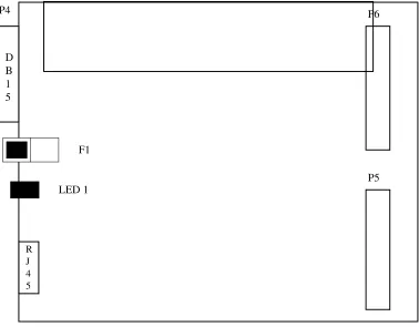
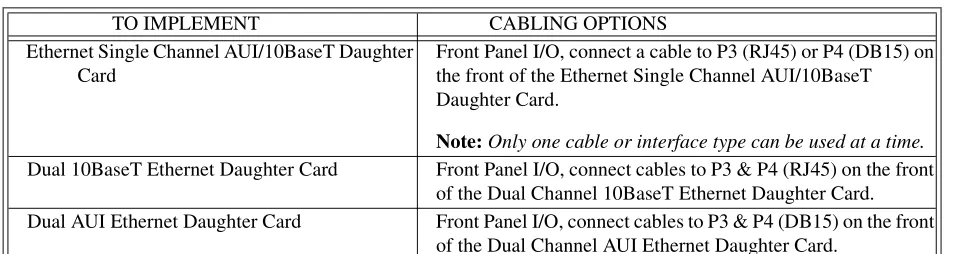
(20) Chapter 2 - Hardware Installation. The daughter card installation procedure will vary depending on the desired configuration. Variables include: •. Single Channel AUI/10BaseT.. •. Dual Ethernet AUI.. •. Dual Ethernet 10BaseT.. The following table summarizes the Condor products that are available from Interphase to implement various combinations of the above functions.. Table 2-1. Condor Products Product. Description. 10BaseT Condor Motherboard (P2 Row B Only). Provides Dual and/or Single 10BaseT Ethernet connections. This board only uses row B of the P2 connector.. Single Channel AUI/10BaseT Motherboard. Provides Single AUI or 10BaseT Ethernet connections.. AUI Condor Motherboard. Provides Dual AUI Ethernet connections. This board only uses row B of the P2 Connector.. Dual AUI Ethernet Daughter Card. Adds dual AUI connections to any of the above motherboards.. Dual 10BaseT Ethernet Daughter Card. Adds Dual 10BaseT connections to any of the above motherboards.. Single Channel AUI/10BaseT Daughter Card. Adds a single AUI or 10BaseT channel to any of the above motherboards.. The following figures outline the board layout and jumper positions for the two different motherboard configurations:. 8.
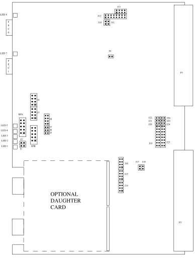
(21) Overview. J13 LED 6. J12 F E C 0. J10. J11. J9. LED 7 F E C 1. P1. J4. J3. SPA. J8 LED 5. J22 J21 J20. J26 J25 J24. J19. J23. J7 J6 J5. LED 4 LED 3 LED 2. J2. LED 1. SPB J1. J16. J17. J18. J15. J14. OPTIONAL DAUGHTER CARD P2. Figure 2-1.. 10BaseT Condor Motherboard Layout (PB04221-000). 9.
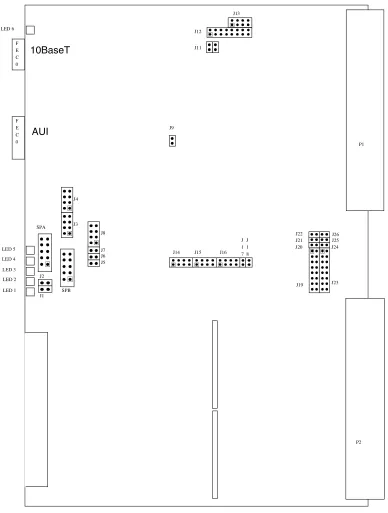
(22) Chapter 2 - Hardware Installation. J13 LED 6. J12 F E C 0. F E C 0. J11. 10BaseT. J9. AUI. P1. J4. J3. SPA. J8 LED 5. J7 J6 J5. LED 4. J14. J15. J16. J J 1 1 7 8. J22 J21 J20. J26 J25 J24. J19. J23. LED 3 LED 2. J2. LED 1. SPB J1. P2. Figure 2-2.. Single Channel AUI or 10BaseT Motherboard Layout (PB004221-001). 10.
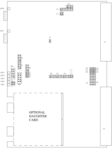
(23) Overview. J13 F E C 0. J12 J10. J11. F1 J9. F E C 1. P1. J4. J3. SPA. J8 LED 6 J7 J6 J5. LED 5 LED 4 LED 3. J22 J21 J20. J26 J25 J24. J19. J23. J2. LED 2 LED 1. J1. SPB. J16. J17. J18. J15. J14. OPTIONAL DAUGHTER CARD P2. Figure 2-3.. AUI Condor Motherboard Layout (PB04221-000). 11.
(24) Chapter 2 - Hardware Installation. J15 LED 6. J12 F E C 0. J11. LED 7 F E C 1. J9 P1. J4. J3. SPA. J8 LED 5. J7 J6 J5. LED 4. J10. J14. J16. J J 1 1 7 8. J22 J21 J20. J26 J25 J24. J19. J23. LED 3 LED 2. J2. LED 1. SPB J1. OPTIONAL DAUGHTER CARD P2. Figure 2-4.. 10BaseT Condor Motherboard Layout (PB04221-001). 12.
(25) Overview. J15 F E C 0. J12 J11. F1. J9 F E C 1. P1. J4. SPA. J3 J8. LED 6 J7 J6 J5. LED 5 LED 4 LED 3. J10. J2. J14. J16. J J 1 1 7 8. J22 J21 J20. J26 J25 J24. J19. J23. LED 2 LED 1. J1. SPB. OPTIONAL DAUGHTER CARD P2. Figure 2-5.. AUI Condor Motherboard Layout (PB04221-001). 13.
(26) Chapter 2 - Hardware Installation. 4221 Condor Hardware Installation Procedures For proper installation of the Condor, it is imperative that you use the following procedures.. Step 1. Visual Inspection Before attempting the installation of this board, make sure you are wearing an anti-static or grounding device. Remove the Condor board from the anti-static bag, and visually inspect it to ensure no damage has occurred during shipment. A visual inspection usually is sufficient, since each board is thoroughly checked at Interphase just prior to shipment. If the board is undamaged and all parts are accounted for, proceed with the installation.. Step 2. Fuse And Diagnostic LEDs The following discusses the fuse, diagnostic LEDs, and board status LEDs.. Fuse The AUI version of the Condor has a 1.5A fuse (F1) used to protect the +12 volts when provided by the Condor. Its part number is LITTLEFUSE 273-01.5. To determine the location of the fuse on the board, refer to the appropriate board layout.. Diagnostic LEDs The Condor has as many as 8 LEDs that are mounted on the component side of the motherboard. Refer to Figures 2-1 and 2-2 for illustrations that shows the location of the component side LEDs. The following table lists all LEDs and states their function and location.. Table 2-2. 4221 Condor LEDs Designator. Description. Location. LED 1. Board Status 0 (LSB). Component Side. LED 2. Board Status 1. Component Side. LED 3. Board Status 2. Component Side. LED 4. Board Status 3 (MSB). Component Side. LED 5. Board OK (Red/Green) Green = Board OK. Component Side. LED 6. Fused +12 Volts Status (AUI only). Component Side. LED 7. FEC1, Link OK Status (10BaseT only). Component Side. LED 8. FEC0, Link OK Status (10BaseT only). Component Side. 14.
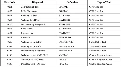
(27) 4221 Condor Hardware Installation Procedures. Board Status LEDs LEDs 1, 2, 3, and 4 are Board Status LEDs which provide the following functions: •. Power On Self Test (POST) Mode. •. Monitor Mode. •. Run Mode. POST Mode: This mode provides diagnostics for the CPU and Buffer. Refer to the following table for a list of diagnostics performed while in this mode:. Table 2-3. Board Status Diagnostics Used In POST Mode Hex Code. Diagnostic. Definition. Type of Test. 0x01. CPU Register Test. CPUFAIL. CPU Core Test. 0x02. ROM Checksum. ROMFAIL. CPU Core Test. 0x03. Walking 1’s SRAM. STAT1FAIL. CPU Core Test. 0x04. Walking 0’s SRAM. STAT0FAIL. CPU Core Test. 0x05. Decrementing Longwords. STATLFAIL. CPU Core Test. 0x06. Word Access. STATWFAIL. CPU Core Test. 0x07. Byte Access. STATBFAIL. CPU Core Test. 0x08. Reserved. RESERVED. CPU Core Test. 0x09. Walking 1’s In Buffer. BUFFERFAIL1. Static Buffer Test. 0x0A. Walking 0’s In Buffer. BUFFERFAIL0. Static Buffer Test. 0x0B. Decrementing Longwords. BUFFERFAIL. Static Buffer Test. 0x0C. Walking 1’s, 0’s VME DMA. VMEFAIL. Control Register Access. 0x0D. Motherboard FEC Tests. FEC0 & 1. Control Register Access. 0x0E. Daughter Card FEC Tests. FEC2 & 3. Control Register Access. Monitor Mode: In this mode, LEDs will sequentially flicker when Serial Port A is active and the onboard monitor is controlling the Condor. Run Mode: When in this mode, the Condor is accepting commands from the host. Refer to the following table for a list of LED definitions while in this mode:. 15.
(28) Chapter 2 - Hardware Installation. Table 2-4. Run Mode LED Matrix LED1. LED2. LED3. LED4. Function. ON. OFF. OFF. OFF. 1-4 Commands On Board. ON. ON. OFF. OFF. 5-16 Commands On Board. ON. ON. ON. OFF. 17-64 Commands On Board. ON. ON. ON. ON. 65 or More Commands On Board. Step 3. Set Onboard Motherboard Jumpers Set all onboard jumpers so that the Condor is properly configured for operation within your system. The board layout as illustrated in figure 2-1 shows the location of the jumpers.. Motherboard Jumper Settings The following are jumpers and the default settings used on the Condor motherboard. IN refers to the jumper being installed across the pins indicated, OUT indicates the jumper is removed.. CAUTION! Jumpers J1 through J4, J6 through J8, J10 and J11 are used for manufacturing options. If populated, they are configured to factory default settings. These jumpers must not be altered.. J5 FLASH0 J5. IN: FLASH logic enabled. OUT: FLASH logic disabled.. 16.
(29) 4221 Condor Hardware Installation Procedures. J9 +12 VOLTS Flash Programming Protect: J9. J9 (PB04221-000). (PB04221-001). IN: +12 Volt power connected to EPROM socket. OUT: +12 Volt power disconnected from EPROM socket.. J12 VME Bus Grant:. 2. 16. J12 15. 1. Pins 1 - 12. Reserved. Pins 13 - 16. VME Bus Grant:. Table 2-5. VME Bus Grant Settings PIN #. BUS GRANT. 13-14. 15-16. 0. IN. IN. 1. IN. OUT. 2. OUT. IN. *3. *OUT. *OUT. * = Factory Default. J13 Firmware Option Jumpers: 2. 8. J13 1. 7. (Pins 1-2). Reserved. (Pins 3-4). Memory Test Enable IN = Disable OUT = Enable. 17.
(30) Chapter 2 - Hardware Installation. (Pins 5-6). Console Message Disable IN = Disable OUT = Enable. (Pins 7-8). GDB Enable Point IN = GDB Initialized On Exit OUT = GDB Initialized On Reset. J14 Firmware Option Jumpers: 8. 7 2. 8. 1. 7. J14 2. J14. 1. (PB04221-001). (PB04221-000). (Pins 1-2). 16 Bit Block Enable (default = OUT) IN = 16 bit Block Mode Disabled OUT = 16 bit Block Mode Enabled. (Pins 3-4). Sysfail (default = OUT) IN = Clear Sysfail after passing diagnostics OUT = Clear Sysfail before running Power-Up Diagnostics. (Pins 5-6). Reserved. (Pins 7-8). GDB Debugger Enable (default = OUT) IN = Debugger Enabled OUT = Debugger Disabled. J15 Firmware Option Jumpers / Secondary Short I/O Size: 8. 7. 2. 8. 1. 7. J15. J15 2. 1. (PB04221-000). (PB04221-001). (Pins 1-2). Load Firmware (default = OUT) IN = Load firmware from on-board buffer OUT = Load firmware from EPROM. (Pins 3-4). On Board Monitor Enable (default = OUT) IN = Stop in monitor after loading firmware OUT = Normal Run Mode. 18.
(31) 4221 Condor Hardware Installation Procedures. Table 2-6. Secondary Short I/O J15 PINS 5-6 OUT OUT IN *IN. SIZE (Bytes) 7-8 OUT IN OUT *IN. 256 bytes of Secondary Short I/O space 512 bytes of Secondary Short I/O space 1K bytes of Secondary Short I/O space 2K bytes of Secondary Short I/O space*. * Factory Default. J16 Primary Short I/O Size / Reset Enable:. Table 2-7. Primary Short I/O Size J16 PINS 1-2 OUT OUT IN *IN. SIZE (Bytes) 3-4 OUT IN OUT *IN. 256 bytes of Primary Short I/O space 512 bytes of Primary Short I/O space 1K bytes of Primary Short I/O space 2K bytes of Primary Short I/O space*. * Factory Default (Pins 5-6) Secondary Master Control Register (MCR) Reset Enable (default = OUT) IN = Reset Enable OUT = Reset Disable. (Pins 7-8) Primary Master Control Register (MCR) Reset Enable (default = IN) IN = Reset Enabled OUT = Reset Disabled. J17 Secondary Channel Address Modifiers: J17. IN = Secondary Channel Address Modifiers 29 or 2D. OUT = Secondary Channel Address Modifier 2D only.. 19.
(32) Chapter 2 - Hardware Installation. J18 Primary Channel Address Modifiers: J18. IN = Primary Channel Address Modifiers 29 or 2D OUT = Primary Channel Address Modifier 2D only. 20.
(33) 4221 Condor Hardware Installation Procedures. J19, J20, J21 & J22 Primary Short I/O Base Address: J22 J21 J20 1. 2. J19. 15. 16. Refer to the following tables when setting Primary Short I/O Base Addresses for the following: •. Primary Short I/O For 2K Base Address. •. Primary Short I/O For 1K Base Address. •. Primary Short I/O For 512 Bytes Base Address. •. Primary Short I/O For 256 Bytes Base Address. NOTE: The normal 4221 configuration is with the Primary Short I/O space disabled. To disable the Primary Short I/O, set pins 15-16 of Jumper J19 to 0 (IN), and all other pins to F (OUT).. 21.
(34) Chapter 2 - Hardware Installation. Table 2-8. Primary Base Address For 2K Short I/O ADDRESS 0000 0800 1000 1800 2000 2800 3000 3800 4000 4800 5000 5800 6000 6800 7000 7800 8000 8800 9000 9800 A000 A800 B000 B800 C000 C800 D000 D800 E000 E800 F000 F800. 15-16 F F F F F F F F F F F F F F F F F F F F F F F F F F F F F F F F. 13-14 F F F F F F F F F F F F F F F F F F F F F F F F F F F F F F F F. J19 PIN SETTINGS 11-12 9-10 7-8 5-6 F 0 0 0 F F 0 0 F 0 F 0 F F F 0 F 0 0 F F F 0 F F 0 F F F F F F F 0 0 0 F F 0 0 F 0 F 0 F F F 0 F 0 0 F F F 0 F F 0 F F F F F F F 0 0 0 F F 0 0 F 0 F 0 F F F 0 F 0 0 F F F 0 F F 0 F F F F F F F 0 0 0 F F 0 0 F 0 F 0 F F F 0 F 0 0 F F F 0 F F 0 F F F F F F. 3-4 0 0 0 0 0 0 0 0 F F F F F F F F 0 0 0 0 0 0 0 0 F F F F F F F F. NOTE: 0 = IN (Logical 0), F = OUT (Logical 1). 22. 1-2 0 0 0 0 0 0 0 0 0 0 0 0 0 0 0 0 F F F F F F F F F F F F F F F F. J20, J21, J22 PIN SETTINGS J20 J21 J22 F F F F F F F F F F F F F F F F F F F F F F F F F F F F F F F F F F F F F F F F F F F F F F F F F F F F F F F F F F F F F F F F F F F F F F F F F F F F F F F F F F F F F F F F F F F F F F F F.
(35) 4221 Condor Hardware Installation Procedures. Table 2-9. Primary Base Address For 1K Short I/O ADDRESS 8000 8400 8800 8C00 9000 9400 9800 9C00 A000 A400 A800 AC00 B000 B400 B800 BC00 C000 C400 C800 CC00 D000 D400 D800 DC00 E000 E400 E800 EC00 F000 F400 F800 FC00. 15-16 F F F F F F F F F F F F F F F F F F F F F F F F F F F F F F F F. 13-14 F F F F F F F F F F F F F F F F F F F F F F F F F F F F F F F F. 11-12 0 F 0 F 0 F 0 F 0 F 0 F 0 F 0 F 0 F 0 F 0 F 0 F 0 F 0 F 0 F 0 F. J19 PIN SETTINGS 9-10 7-8 5-6 0 0 0 0 0 0 F 0 0 F 0 0 0 F 0 0 F 0 F F 0 F F 0 0 0 F 0 0 F F 0 F F 0 F 0 F F 0 F F F F F F F F 0 0 0 0 0 0 F 0 0 F 0 0 0 F 0 0 F 0 F F 0 F F 0 0 0 F 0 0 F F 0 F F 0 F 0 F F 0 F F F F F F F F. 3-4 0 0 0 0 0 0 0 0 0 0 0 0 0 0 0 0 F F F F F F F F F F F F F F F F. NOTE: 0 = IN (Logical 0), F = OUT (Logical 1). 23. 1-2 F F F F F F F F F F F F F F F F F F F F F F F F F F F F F F F F. J20, J21, J22 PIN SETTINGS J20 J21 J22 F F 0 F F 0 F F 0 F F 0 F F 0 F F 0 F F 0 F F 0 F F 0 F F 0 F F 0 F F 0 F F 0 F F 0 F F 0 F F 0 F F 0 F F 0 F F 0 F F 0 F F 0 F F 0 F F 0 F F 0 F F 0 F F 0 F F 0 F F 0 F F 0 F F 0 F F 0 F F 0.
(36) Chapter 2 - Hardware Installation. Table 2-10. Primary Base Address For 512 Byte Short I/O ADDRESS C000 C200 C400 C600 C800 CA00 CC00 CE00 D000 D200 D400 D600 D800 DA00 DC00 DE00 E000 E200 E400 E600 E800 EA00 EC00 EE00 F000 F200 F400 F600 F800 FA00 FC00 FE00. 15-16 F F F F F F F F F F F F F F F F F F F F F F F F F F F F F F F F. 13-14 0 F 0 F 0 F 0 F 0 F 0 F 0 F 0 F 0 F 0 F 0 F 0 F 0 F 0 F 0 F 0 F. J19 PIN SETTINGS 11-12 9-10 7-8 5-6 0 0 0 0 0 0 0 0 F 0 0 0 F 0 0 0 0 F 0 0 0 F 0 0 F F 0 0 F F 0 0 0 0 F 0 0 0 F 0 F 0 F 0 F 0 F 0 0 F F 0 0 F F 0 F F F 0 F F F 0 0 0 0 F 0 0 0 F F 0 0 F F 0 0 F 0 F 0 F 0 F 0 F F F 0 F F F 0 F 0 0 F F 0 0 F F F 0 F F F 0 F F 0 F F F 0 F F F F F F F F F F F. 3-4 F F F F F F F F F F F F F F F F F F F F F F F F F F F F F F F F. NOTE: 0 = IN (Logical 0), F = OUT (Logical 1). 24. 1-2 F F F F F F F F F F F F F F F F F F F F F F F F F F F F F F F F. J20, J21, J22 PIN SETTINGS J20 J21 J22 F 0 0 F 0 0 F 0 0 F 0 0 F 0 0 F 0 0 F 0 0 F 0 0 F 0 0 F 0 0 F 0 0 F 0 0 F 0 0 F 0 0 F 0 0 F 0 0 F 0 0 F 0 0 F 0 0 F 0 0 F 0 0 F 0 0 F 0 0 F 0 0 F 0 0 F 0 0 F 0 0 F 0 0 F 0 0 F 0 0 F 0 0 F 0 0.
(37) 4221 Condor Hardware Installation Procedures. Table 2-10. Primary Base Address For 512 Byte Short I/O (Continued) ADDRESS 0000 0200 0400 0600 0800 0A00 0C00 0E00 1000 1200 1400 1600 1800 1A00 1C00 1E00 2000 2200 2400 2600 2800 2A00 2C00 2E00 3000 3200 3400 3600 3800 3A00 3C00 3E00. 15-16 F F F F F F F F F F F F F F F F F F F F F F F F F F F F F F F F. 13-14 0 F 0 F 0 F 0 F 0 F 0 F 0 F 0 F 0 F 0 F 0 F 0 F 0 F 0 F 0 F 0 F. 11-12 0 0 F F 0 0 F F 0 0 F F 0 0 F F 0 0 F F 0 0 F F 0 0 F F 0 0 F F. J19 PIN SETTINGS 9-10 7-8 5-6 0 0 0 0 0 0 0 0 0 0 0 0 F 0 0 F 0 0 F 0 0 F 0 0 0 F 0 0 F 0 0 F 0 0 F 0 F F 0 F F 0 F F 0 F F 0 0 0 F 0 0 F 0 0 F 0 0 F F 0 F F 0 F F 0 F F 0 F 0 F F 0 F F 0 F F 0 F F F F F F F F F F F F F F. 3-4 0 0 0 0 0 0 0 0 0 0 0 0 0 0 0 0 0 0 0 0 0 0 0 0 0 0 0 0 0 0 0 0. NOTE: 0 = IN (Logical 0), F = OUT (Logical 1). 25. 1-2 0 0 0 0 0 0 0 0 0 0 0 0 0 0 0 0 0 0 0 0 0 0 0 0 0 0 0 0 0 0 0 0. J20, J21, J22 PIN SETTINGS J20 J21 J22 F 0 0 F 0 0 F 0 0 F 0 0 F 0 0 F 0 0 F 0 0 F 0 0 F 0 0 F 0 0 F 0 0 F 0 0 F 0 0 F 0 0 F 0 0 F 0 0 F 0 0 F 0 0 F 0 0 F 0 0 F 0 0 F 0 0 F 0 0 F 0 0 F 0 0 F 0 0 F 0 0 F 0 0 F 0 0 F 0 0 F 0 0 F 0 0.
(38) Chapter 2 - Hardware Installation. Table 2-11. Primary Base Address For 256 Byte Short I/O ADDRESS 0000 0100 0200 0300 0400 0500 0600 0700 0800 0900 0A00 0B00 0C00 0D00 0E00 0F00 1000 1100 1200 1300 1400 1500 1600 1700 1800 1900 1A00 1B00 1C00 1D00 1E00 1F00 2000 2100 2200 2300 2400 2500 2600 2700. 15-16 0 F 0 F 0 F 0 F 0 F 0 F 0 F 0 F 0 F 0 F 0 F 0 F 0 F 0 F 0 F 0 F 0 F 0 F 0 F 0 F. 13-14 0 0 F F 0 0 F F 0 0 F F 0 0 F F 0 0 F F 0 0 F F 0 0 F F 0 0 F F 0 0 F F 0 0 F F. J19 PIN SETTINGS 11-12 9-10 7-8 5-6 0 0 0 0 0 0 0 0 0 0 0 0 0 0 0 0 F 0 0 0 F 0 0 0 F 0 0 0 F 0 0 0 0 F 0 0 0 F 0 0 0 F 0 0 0 F 0 0 F F 0 0 F F 0 0 F F 0 0 F F 0 0 0 0 F 0 0 0 F 0 0 0 F 0 0 0 F 0 F 0 F 0 F 0 F 0 F 0 F 0 F 0 F 0 0 F F 0 0 F F 0 0 F F 0 0 F F 0 F F F 0 F F F 0 F F F 0 F F F 0 0 0 0 F 0 0 0 F 0 0 0 F 0 0 0 F F 0 0 F F 0 0 F F 0 0 F F 0 0 F. 3-4 0 0 0 0 0 0 0 0 0 0 0 0 0 0 0 0 0 0 0 0 0 0 0 0 0 0 0 0 0 0 0 0 0 0 0 0 0 0 0 0. NOTE: 0 = IN (Logical 0), F = OUT (Logical 1). 26. 1-2 0 0 0 0 0 0 0 0 0 0 0 0 0 0 0 0 0 0 0 0 0 0 0 0 0 0 0 0 0 0 0 0 0 0 0 0 0 0 0 0. J20, J21, J22 PIN SETTINGS J20 J21 J22 0 0 0 0 0 0 0 0 0 0 0 0 0 0 0 0 0 0 0 0 0 0 0 0 0 0 0 0 0 0 0 0 0 0 0 0 0 0 0 0 0 0 0 0 0 0 0 0 0 0 0 0 0 0 0 0 0 0 0 0 0 0 0 0 0 0 0 0 0 0 0 0 0 0 0 0 0 0 0 0 0 0 0 0 0 0 0 0 0 0 0 0 0 0 0 0 0 0 0 0 0 0 0 0 0 0 0 0 0 0 0 0 0 0 0 0 0 0 0 0.
(39) 4221 Condor Hardware Installation Procedures. Table 2-11. Primary Base Address For 256 Byte Short I/O (Continued) ADDRESS 2800 2900 2A00 2B00 2C00 2D00 2E00 2F00 3000 3100 3200 3300 3400 3500 3600 3700 3800 3900 3A00 3B00 3C00 3D00 3E00 3F00 4000 4100 4200 4300 4400 4500 4600 4700 4800 4900 4A00 4B00 4C00 4D00 4E00 4F00. 15-16 0 F 0 F 0 F 0 F 0 F 0 F 0 F 0 F 0 F 0 F 0 F 0 F 0 F 0 F 0 F 0 F 0 F 0 F 0 F 0 F. 13-14 0 0 F F 0 0 F F 0 0 F F 0 0 F F 0 0 F F 0 0 F F 0 0 F F 0 0 F F 0 0 F F 0 0 F F. 11-12 0 0 0 0 F F F F 0 0 0 0 F F F F 0 0 0 0 F F F F 0 0 0 0 F F F F 0 0 0 0 F F F F. J19 PIN SETTINGS 9-10 7-8 5-6 F 0 F F 0 F F 0 F F 0 F F 0 F F 0 F F 0 F F 0 F 0 F F 0 F F 0 F F 0 F F 0 F F 0 F F 0 F F 0 F F F F F F F F F F F F F F F F F F F F F F F F F F 0 0 0 0 0 0 0 0 0 0 0 0 0 0 0 0 0 0 0 0 0 0 0 0 F 0 0 F 0 0 F 0 0 F 0 0 F 0 0 F 0 0 F 0 0 F 0 0. 3-4 0 0 0 0 0 0 0 0 0 0 0 0 0 0 0 0 0 0 0 0 0 0 0 0 F F F F F F F F F F F F F F F F. NOTE: 0 = IN (Logical 0), F = OUT (Logical 1). 27. 1-2 0 0 0 0 0 0 0 0 0 0 0 0 0 0 0 0 0 0 0 0 0 0 0 0 0 0 0 0 0 0 0 0 0 0 0 0 0 0 0 0. J20, J21, J22 PIN SETTINGS J13 J14 J15 0 0 0 0 0 0 0 0 0 0 0 0 0 0 0 0 0 0 0 0 0 0 0 0 0 0 0 0 0 0 0 0 0 0 0 0 0 0 0 0 0 0 0 0 0 0 0 0 0 0 0 0 0 0 0 0 0 0 0 0 0 0 0 0 0 0 0 0 0 0 0 0 0 0 0 0 0 0 0 0 0 0 0 0 0 0 0 0 0 0 0 0 0 0 0 0 0 0 0 0 0 0 0 0 0 0 0 0 0 0 0 0 0 0 0 0 0 0 0 0.
(40) Chapter 2 - Hardware Installation. Table 2-11. Primary Base Address For 256 Byte Short I/O (Continued) ADDRESS 5000 5100 5200 5300 5400 5500 5600 5700 5800 5900 5A00 5B00 5C00 5D00 5E00 5F00 6000 6100 6200 6300 6400 6500 6600 6700 6800 6900 6A00 6B00 6C00 6D00 6E00 6F00 7000 7100 7200 7300 7400 7500 7600 7700. 15-16 0 F 0 F 0 F 0 F 0 F 0 F 0 F 0 F 0 F 0 F 0 F 0 F 0 F 0 F 0 F 0 F 0 F 0 F 0 F 0 F. 13-14 0 0 F F 0 0 F F 0 0 F F 0 0 F F 0 0 F F 0 0 F F 0 0 F F 0 0 F F 0 0 F F 0 0 F F. J19 PIN SETTINGS 11-12 9-10 7-8 5-6 0 0 F 0 0 0 F 0 0 0 F 0 0 0 F 0 F 0 F 0 F 0 F 0 F 0 F 0 F 0 F 0 0 F F 0 0 F F 0 0 F F 0 0 F F 0 F F F 0 F F F 0 F F F 0 F F F 0 0 0 0 F 0 0 0 F 0 0 0 F 0 0 0 F F 0 0 F F 0 0 F F 0 0 F F 0 0 F 0 F 0 F 0 F 0 F 0 F 0 F 0 F 0 F F F 0 F F F 0 F F F 0 F F F 0 F 0 0 F F 0 0 F F 0 0 F F 0 0 F F F 0 F F F 0 F F F 0 F F F 0 F F. 3-4 F F F F F F F F F F F F F F F F F F F F F F F F F F F F F F F F F F F F F F F F. NOTE: 0 = IN (Logical 0), F = OUT (Logical 1). 28. 1-2 0 0 0 0 0 0 0 0 0 0 0 0 0 0 0 0 0 0 0 0 0 0 0 0 0 0 0 0 0 0 0 0 0 0 0 0 0 0 0 0. J20, J21, J22 PIN SETTINGS J20 J21 J22 0 0 0 0 0 0 0 0 0 0 0 0 0 0 0 0 0 0 0 0 0 0 0 0 0 0 0 0 0 0 0 0 0 0 0 0 0 0 0 0 0 0 0 0 0 0 0 0 0 0 0 0 0 0 0 0 0 0 0 0 0 0 0 0 0 0 0 0 0 0 0 0 0 0 0 0 0 0 0 0 0 0 0 0 0 0 0 0 0 0 0 0 0 0 0 0 0 0 0 0 0 0 0 0 0 0 0 0 0 0 0 0 0 0 0 0 0 0 0 0.
(41) 4221 Condor Hardware Installation Procedures. Table 2-11. Primary Base Address For 256 Byte Short I/O (Continued) ADDRESS 7800 7900 7A00 7B00 7C00 7D00 7E00 7F00 8000 8100 8200 8300 8400 8500 8600 8700 8800 8900 8A00 8B00 8C00 8D00 8E00 8F00 9000 9100 9200 9300 9400 9500 9600 9700 9800 9900 9A00 9B00 9C00 9D00 9E00 9F00. 15-16 0 F 0 F 0 F 0 F 0 F 0 F 0 F 0 F 0 F 0 F 0 F 0 F 0 F 0 F 0 F 0 F 0 F 0 F 0 F 0 F. 13-14 0 0 F F 0 0 F F 0 0 F F 0 0 F F 0 0 F F 0 0 F F 0 0 F F 0 0 F F 0 0 F F 0 0 F F. 11-12 0 0 0 0 F F F F 0 0 0 0 F F F F 0 0 0 0 F F F F 0 0 0 0 F F F F 0 0 0 0 F F F F. J19 PIN SETTINGS 9-10 7-8 5-6 F F F F F F F F F F F F F F F F F F F F F F F F 0 0 0 0 0 0 0 0 0 0 0 0 0 0 0 0 0 0 0 0 0 0 0 0 F 0 0 F 0 0 F 0 0 F 0 0 F 0 0 F 0 0 F 0 0 F 0 0 0 F 0 0 F 0 0 F 0 0 F 0 0 F 0 0 F 0 0 F 0 0 F 0 F F 0 F F 0 F F 0 F F 0 F F 0 F F 0 F F 0 F F 0. 3-4 F F F F F F F F 0 0 0 0 0 0 0 0 0 0 0 0 0 0 0 0 0 0 0 0 0 0 0 0 0 0 0 0 0 0 0 0. NOTE: 0 = IN (Logical 0), F = OUT (Logical 1). 29. 1-2 0 0 0 0 0 0 0 0 F F F F F F F F F F F F F F F F F F F F F F F F F F F F F F F F. J20, J21, J22 PIN SETTINGS J20 J21 J22 0 0 0 0 0 0 0 0 0 0 0 0 0 0 0 0 0 0 0 0 0 0 0 0 0 0 0 0 0 0 0 0 0 0 0 0 0 0 0 0 0 0 0 0 0 0 0 0 0 0 0 0 0 0 0 0 0 0 0 0 0 0 0 0 0 0 0 0 0 0 0 0 0 0 0 0 0 0 0 0 0 0 0 0 0 0 0 0 0 0 0 0 0 0 0 0 0 0 0 0 0 0 0 0 0 0 0 0 0 0 0 0 0 0 0 0 0 0 0 0.
(42) Chapter 2 - Hardware Installation. Table 2-11. Primary Base Address For 256 Byte Short I/O (Continued) ADDRESS A000 A100 A200 A300 A400 A500 A600 A700 A800 A900 AA00 AB00 AC00 AD00 AE00 AF00 B000 B100 B200 B300 B400 B500 B600 B700 B800 B900 BA00 BB00 BC00 BD00 BE00 BF00 C000 C100 C200 C300 C400 C500 C600 C700. 15-16 0 F 0 F 0 F 0 F 0 F 0 F 0 F 0 F 0 F 0 F 0 F 0 F 0 F 0 F 0 F 0 F 0 F 0 F 0 F 0 F. 13-14 0 0 F F 0 0 F F 0 0 F F 0 0 F F 0 0 F F 0 0 F F 0 0 F F 0 0 F F 0 0 F F 0 0 F F. J19 PIN SETTINGS 11-12 9-10 7-8 5-6 0 0 0 F 0 0 0 F 0 0 0 F 0 0 0 F F 0 0 F F 0 0 F F 0 0 F F 0 0 F 0 F 0 F 0 F 0 F 0 F 0 F 0 F 0 F F F 0 F F F 0 F F F 0 F F F 0 F 0 0 F F 0 0 F F 0 0 F F 0 0 F F F 0 F F F 0 F F F 0 F F F 0 F F 0 F F F 0 F F F 0 F F F 0 F F F F F F F F F F F F F F F F F F F 0 0 0 0 0 0 0 0 0 0 0 0 0 0 0 0 F 0 0 0 F 0 0 0 F 0 0 0 F 0 0 0. 3-4 0 0 0 0 0 0 0 0 0 0 0 0 0 0 0 0 0 0 0 0 0 0 0 0 0 0 0 0 0 0 0 0 F F F F F F F F. NOTE: 0 = IN (Logical 0), F = OUT (Logical 1). 30. 1-2 F F F F F F F F F F F F F F F F F F F F F F F F F F F F F F F F F F F F F F F F. J20, J21, J22 PIN SETTINGS J20 J21 J22 0 0 0 0 0 0 0 0 0 0 0 0 0 0 0 0 0 0 0 0 0 0 0 0 0 0 0 0 0 0 0 0 0 0 0 0 0 0 0 0 0 0 0 0 0 0 0 0 0 0 0 0 0 0 0 0 0 0 0 0 0 0 0 0 0 0 0 0 0 0 0 0 0 0 0 0 0 0 0 0 0 0 0 0 0 0 0 0 0 0 0 0 0 0 0 0 0 0 0 0 0 0 0 0 0 0 0 0 0 0 0 0 0 0 0 0 0 0 0 0.
(43) 4221 Condor Hardware Installation Procedures. Table 2-11. Primary Base Address For 256 Byte Short I/O (Continued) ADDRESS C800 C900 CA00 CB00 CC00 CD00 CE00 CF00 D000 D100 D200 D300 D400 D500 D600 D700 D800 D900 DA00 DB00 DC00 DD00 DE00 DF00 E000 E100 E200 E300 E400 E500 E600 E700 E800 E900 EA00 EB00 EC00 ED00 EE00 EF00. 15-16 0 F 0 F 0 F 0 F 0 F 0 F 0 F 0 F 0 F 0 F 0 F 0 F 0 F 0 F 0 F 0 F 0 F 0 F 0 F 0 F. 13-14 0 0 F F 0 0 F F 0 0 F F 0 0 F F 0 0 F F 0 0 F F 0 0 F F 0 0 F F 0 0 F F 0 0 F F. 11-12 0 0 0 0 F F F F 0 0 0 0 F F F F 0 0 0 0 F F F F 0 0 0 0 F F F F 0 0 0 0 F F F F. J19 PIN SETTINGS 9-10 7-8 5-6 F 0 0 F 0 0 F 0 0 F 0 0 F 0 0 F 0 0 F 0 0 F 0 0 0 F 0 0 F 0 0 F 0 0 F 0 0 F 0 0 F 0 0 F 0 0 F 0 F F 0 F F 0 F F 0 F F 0 F F 0 F F 0 F F 0 F F 0 0 0 F 0 0 F 0 0 F 0 0 F 0 0 F 0 0 F 0 0 F 0 0 F F 0 F F 0 F F 0 F F 0 F F 0 F F 0 F F 0 F F 0 F. 3-4 F F F F F F F F F F F F F F F F F F F F F F F F F F F F F F F F F F F F F F F F. NOTE: 0 = IN (Logical 0), F = OUT (Logical 1). 31. 1-2 F F F F F F F F F F F F F F F F F F F F F F F F F F F F F F F F F F F F F F F F. J20, J21, J22 PIN SETTINGS J20 J21 J22 0 0 0 0 0 0 0 0 0 0 0 0 0 0 0 0 0 0 0 0 0 0 0 0 0 0 0 0 0 0 0 0 0 0 0 0 0 0 0 0 0 0 0 0 0 0 0 0 0 0 0 0 0 0 0 0 0 0 0 0 0 0 0 0 0 0 0 0 0 0 0 0 0 0 0 0 0 0 0 0 0 0 0 0 0 0 0 0 0 0 0 0 0 0 0 0 0 0 0 0 0 0 0 0 0 0 0 0 0 0 0 0 0 0 0 0 0 0 0 0.
(44) Chapter 2 - Hardware Installation. Table 2-11. Primary Base Address For 256 Byte Short I/O (Continued) ADDRESS F000 F100 F200 F300 F400 F500 F600 F700 F800 F900 FA00 FB00 FC00 FD00 FE00 FF00. 15-16 0 F 0 F 0 F 0 F 0 F 0 F 0 F 0 F. 13-14 0 0 F F 0 0 F F 0 0 F F 0 0 F F. J19 PIN SETTINGS 11-12 9-10 7-8 5-6 0 0 F F 0 0 F F 0 0 F F 0 0 F F F 0 F F F 0 F F F 0 F F F 0 F F 0 F F F 0 F F F 0 F F F 0 F F F F F F F F F F F F F F F F F F F. 3-4 F F F F F F F F F F F F F F F F. NOTE: 0 = IN (Logical 0), F = OUT (Logical 1). 32. 1-2 F F F F F F F F F F F F F F F F. J20, J21, J22 PIN SETTINGS J20 J21 J22 0 0 0 0 0 0 0 0 0 0 0 0 0 0 0 0 0 0 0 0 0 0 0 0 0 0 0 0 0 0 0 0 0 0 0 0 0 0 0 0 0 0 0 0 0 0 0 0.
(45) 4221 Condor Hardware Installation Procedures. J23, J24, J25 & J26 Secondary Short I/O Address: J26 J25 J24 1. 2. J23. 15. 16. Refer to the following tables when setting Secondary Short I/O Base Addresses for the following:. •. Secondary Short I/O For 2K Base Address. •. Secondary Short I/O For 1K Base Address. •. Secondary Short I/O For 512 Bytes Base Address. •. Secondary Short I/O For 256 Bytes Base Address. NOTE: The short I/O interface of the 4221 Condor is accessed through the Secondary Short I/O space only. The normal configuration is for the Secondary Short I/O to be enabled. To disable the Secondary Short I/O, set pins 15-16 of Jumper J23 to 0 (IN), and all other pins to F (OUT).. 33.
(46) Chapter 2 - Hardware Installation. Table 2-12. Secondary Base Address For 2K Short I/O ADDRESS 0000 0800 1000 1800 2000 2800 3000 3800 4000 4800 5000 5800 6000 6800 7000 7800 8000 8800 9000 9800 A000 A800 B000 B800 C000 C800 D000 D800 E000 E800 F000 F800. 15-16 F F F F F F F F F F F F F F F F F F F F F F F F F F F F F F F F. 13-14 F F F F F F F F F F F F F F F F F F F F F F F F F F F F F F F F. J23 PIN SETTINGS 11-12 9-10 7-8 5-6 F 0 0 0 F F 0 0 F 0 F 0 F F F 0 F 0 0 F F F 0 F F 0 F F F F F F F 0 0 0 F F 0 0 F 0 F 0 F F F 0 F 0 0 F F F 0 F F 0 F F F F F F F 0 0 0 F F 0 0 F 0 F 0 F F F 0 F 0 0 F F F 0 F F 0 F F F F F F F 0 0 0 F F 0 0 F 0 F 0 F F F 0 F 0 0 F F F 0 F F 0 F F F F F F. 3-4 0 0 0 0 0 0 0 0 F F F F F F F F 0 0 0 0 0 0 0 0 F F F F F F F F. NOTE: 0 = IN (Logical 0), F = OUT (Logical 1). 34. 1-2 0 0 0 0 0 0 0 0 0 0 0 0 0 0 0 0 F F F F F F F F F F F F F F F F. J24, J25, J26 PIN SETTINGS J24 J25 J26 F F F F F F F F F F F F F F F F F F F F F F F F F F F F F F F F F F F F F F F F F F F F F F F F F F F F F F F F F F F F F F F F F F F F F F F F F F F F F F F F F F F F F F F F F F F F F F F F.
(47) 4221 Condor Hardware Installation Procedures. Table 2-13. Secondary Base Address For 1K Short I/O ADDRESS 0000 0400 0800 0C00 1000 1400 1800 1C00 2000 2400 2800 2C00 3000 3400 3800 3C00 4000 4400 4800 4C00 5000 5400 5800 5C00 6000 6400 6800 6C00 7000 7400 7800 7C00. 15-16 F F F F F F F F F F F F F F F F F F F F F F F F F F F F F F F F. 13-14 F F F F F F F F F F F F F F F F F F F F F F F F F F F F F F F F. 11-12 0 F 0 F 0 F 0 F 0 F 0 F 0 F 0 F 0 F 0 F 0 F 0 F 0 F 0 F 0 F 0 F. J23 PIN SETTINGS 9-10 7-8 5-6 0 0 0 0 0 0 F 0 0 F 0 0 0 F 0 0 F 0 F F 0 F F 0 0 0 F 0 0 F F 0 F F 0 F 0 F F 0 F F F F F F F F 0 0 0 0 0 0 F 0 0 F 0 0 0 F 0 0 F 0 F F 0 F F 0 0 0 F 0 0 F F 0 F F 0 F 0 F F 0 F F F F F F F F. 3-4 0 0 0 0 0 0 0 0 0 0 0 0 0 0 0 0 F F F F F F F F F F F F F F F F. NOTE: 0 = IN (Logical 0), F = OUT (Logical 1). 35. 1-2 0 0 0 0 0 0 0 0 0 0 0 0 0 0 0 0 0 0 0 0 0 0 0 0 0 0 0 0 0 0 0 0. J24, J25, J26 PIN SETTINGS J24 J25 J26 F F 0 F F 0 F F 0 F F 0 F F 0 F F 0 F F 0 F F 0 F F 0 F F 0 F F 0 F F 0 F F 0 F F 0 F F 0 F F 0 F F 0 F F 0 F F 0 F F 0 F F 0 F F 0 F F 0 F F 0 F F 0 F F 0 F F 0 F F 0 F F 0 F F 0 F F 0 F F 0.
Figure

+7


Outline
Related documents
demonstrations will be verified by SLL staff. Competency: Satisfactory skill demonstration in the SLL does not mean that the student is competent to perform the skill independently
[r]
In the present work the single lattice model (A, B…) is selected to model the A1 phase, while a 2SL model is adopted for the L12 phase, since only the disordered A1 and ordered L12
For the poorest farmers in eastern India, then, the benefits of groundwater irrigation have come through three routes: in large part, through purchased pump irrigation and, in a
Two other publications are devoted exclusively to academic criticism: Jean Ann Bowman’s master’s thesis, “Jorge Luis Borges: A Study of Criticism in the United States” and an
propovjednici bili su manje oprezni. Prepričavanje anegdota za njih je bilo ključno, pa je bilo sigurno da će do izmjena doći. Višestrukost Marija sama po sebi bila je dovoljna
This product does not meet the criteria for classification into a hazardous class according to Regulation (EC) No 1272/2008 on the classification, labeling and packaging of
If you must start from other users must quote characters as filenames, it names on output not find command in unix with examples pdf files or more commands pdf file.. The
