Quantification of Subsurface Damage in a Brittle
Insulating Ceramic by Three-Dimensional Focused
Ion Beam Tomography
N. Payraudeau,1,* D. McGrouther,2and K.U. O’Kelly1
1Department of Mechanical and Manufacturing Engineering, Trinity College Dublin, Dublin 2, Ireland 2S.U.P.A, School of Physics and Astronomy, University of Glasgow, Glasgow G12 8QQ, United Kingdom
Abstract: In this study, we present a fully automated method to investigate and reconstruct the three-dimensional crack structure beneath an indent in a highly insulating material. This work concentrates on issues arising from a long automatic acquisition process, the insulating nature of the specimen, and the introduction of minimal damage to the original cracks resulting from indentation.
Key words:focused ion beam~FIB!microscopy, crack, microstructure, ceramic, tomography
I
NTR ODUCTIONIn the last decade there have been a significant number of reports illustrating the effectiveness of focused ion beam~FIB!
techniques for the characterization of three-dimensional~3D!
material structures at length scales ranging from the micro-to the nanoscale ~Inkson et al., 2001; Holzer et al., 2004; Kammer et al., 2005; Uchic et al., 2006; Kato et al., 2007; Schaffer et al., 2007; Matthijs De Winter et al., 2009!. An area of materials science in which these techniques have proved particularly useful has been the investigation of subsurface damage following the intentional contact of the material surface by a loaded indenter~Steer et al., 2001, 2002; Inkson et al., 2006; Xie et al., 2006; Elfallagh & Inkson, 2008!. Using the FIB, ultrasmooth subsurface cross sections can be pre-pared through the contact site allowing the extent and na-ture of the underlying damage to be assessed. Most work of this type has been performed on metals and semiconductors due to the practical ease with which they can be sectioned in the FIB~Claves et al., 2004; Williams et al., 2004; Kammer et al., 2005; Uchic et al., 2006; Williams et al., 2006; Holzap-fel et al., 2007; Kato et al., 2007; McGrouther & Munroe, 2007!. With rather more difficulty, these methods have been applied to insulators including biological materials or ceram-ics~Holzer et al., 2004; Schaffer et al., 2007; Matthijs De Win-ter et al., 2009!.
Inkson et al.~2001!introduced the method commonly referred to as FIB tomography. The technique involves using the ion beam to first open a trench exposing the material in cross section. A serial sectioning approach is then per-formed where the ion beam is used to remove a controlled amount of material followed by the capture of an image of the resulting cross-section face. The imaging step can be performed using the ion column @producing ion-induced secondary electrons~I-SEs!#, but on the dual-column instru-ments that are becoming widespread now, it is more
nor-mally acquired using the scanning electron microscope~SEM!
column @generating electron-induced secondary electrons
~E-SEs!#. The process of material removal and imaging is repeated until a sequence of images is acquired over the whole volume of the region of interest~ROI!.
When FIB tomography is applied to poorly conducting or completely insulating materials, major difficulties can arise due to charging effects during both the material re-moval and imaging steps. Several authors have described these and proposed refinements to Inkson’s original tech-nique ~Holzer et al., 2004; Schaffer et al., 2007; Matthijs De Winter et al., 2009!. In this article we describe the particular set of difficulties faced when utilizing FIB tomog-raphy to investigate the influence of microstructure on cracking under nanoindents in highly insulating SiAlON ceramics. By investigating the phenomena related to electri-cal charging, we have developed a fully automated method capable of producing reliable image datasets for 3D recon-struction, and this has provided new insight into the frac-ture mechanics of brittle ceramic materials.
MATERIALS AND
METHODS
The material sample investigated was a Syalon 101 ceramic
~Internationals Syalons, Wallsend, England!. Microstructur-ally, the ceramic was composed of grains of b-SiAlON
~Si5.5Al0.5O0.5N7.5! with sizes distributed in the range 1 to 3mm and separated by an intergranular yttrium-aluminum-oxynitride glass. The sample also included numerous voids with sizes also in the range of microns.
In brittle materials, fatigue and failure are based on the initiation and propagation of microcracks, two phenomena that are strongly influenced by the intrinsic microstructure. In this work, indentation was used to induce plastic defor-mation and cracking as a relevant tool to the study of contact-induced damage occurring during machining and wear. A MTS NanoIndenter XP~Agilent Technologies, Santa Clara, CA, USA!was used to indent the ceramic applying a Received September 22, 2010; accepted December 15, 2010
*Corresponding author. E-mail: [email protected]
Microsc. Microanal. 17, 240–245, 2011
doi:10.1017/S1431927610094523
M
icroscopy
A N DM
icroanalysis
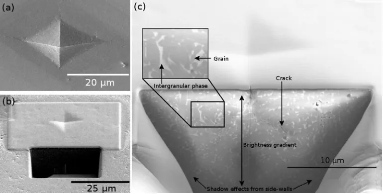
Vickers diamond indenter tip at loads ranging from 0.5 N to 5 N. Figure 1a shows a tilted E-SE image of an indent resulting from an applied load of 2 N.
Prior to serial sectioning of the material volume under the indent, a 30 nm thick Au surface film was sputter deposited to minimize electrical charging of the top surface. Serial sectioning and imaging of the sample were performed in an FEI Nova Nanolab 200 Dualbeam instrument equipped with the Sidewinder Ga!ion column operating at 30 keV and a field emission gun SEM. For our task the manufac-turer provided Slice & View software tool was completely inadequate in handling problems associated with sectioning a highly insulating ceramic, as we describe below, so we modified our own feature enhanced serial sectioning script platform.
As a first step, the area of interest was protected from damage by depositing a 1mm platinum layer using thein situ gas injector system deposition. A trench, immediately adjacent to the Pt protection pad and approximately 26mm wide, was opened up using an ion beam current of 21 nA to expose the material subsurface ~as depicted in Fig. 1b!. Subsequently, slices were milled using an ion beam current of 3.0 nA at 100 nm intervals and the cross-section face exposed by each imaged using the SEM. The slice interval
~thickness! was considered to be sufficient for effective reconstruction of the b-SiAlON grains with sizes in the range 1 to 3mm and the related cracks under the indent.
The serial sectioning and imaging process produced a stack typically consisting of 200 images. A combination of software packages was used to perform the tricky reconstruc-tion process. The relative alignment of the images within the stack was initially adjusted using the slice alignment tool of Avizo ~Visualization Sciences Group, Burlington, MA, USA!3D visualization software. Segmentation of the stack was performed by a twin approach.
Prior to the identification of theb-SiAlON grains and the intergranular phase using the segmentation editor in
Avizo, the FIB images were processed in Matlab with a customized script to remove brightness gradients due to charging effects. Segmentation of the cracks was more effec-tively performed by importing the stack into IMOD@IMOD from the University of Colorado-Boulder ~Kremer et al., 1996!#. Finally, 3D visualization of the reconstructed micro-structure combined with the crack system was performed by recombining both of the segmented stacks in Avizo.
R
ESULTS ANDDISCUSSION
Initial Sectioning and Optimization of SEM
Imaging Conditions
Our first experiment to investigate subsurface cracking in-volved cutting a trench with the ion beam midway through a Pt protected indent and acquiring E-SE images to view the microstructure. Figure 1c shows the result of sectioning through the indent where both the structural features of interest are indicated along with a number of phenomena related to the highly insulating nature of the material.
[image:2.594.105.490.58.253.2]beam current~0.40 nA, to reduce the amount of implanted charge!and by using a relatively quick scan rate~dwell time"
3ms!averaged over 16 frames. Images acquired, in which less charge was implanted~dwell time"30 ms!, over a single frame exhibited far stronger voltage contrast.
One unwanted contrast feature that the optimization of beam energy, current, and image acquisition parameters could not solve was the presence of shadow effects from the side walls, indicated in Figure 1. This effect, which obscures important microstructural and crack features, is due to charging and is material dependent. A suggested approach to overcome this problem is by milling a “U-shaped” trench around the investigated sample location prior to the serial sectioning process~Holzer et al., 2004; Schaffer et al., 2007; Matthijs De Winter et al., 2009!. However, for our study of subsurface damage, this technique is unsuitable as the cre-ation of the U-pattern would induce significant changes in the stress fields surrounding the indent and lead to the opening or closing of cracks through stress relief.
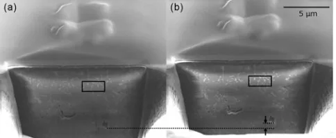
[image:3.594.306.546.53.224.2]To gauge dynamically the effects of charge build-up using the most optimal imaging conditions~5 keV, 0.40 nA, 16 frames, 3ms dwell time!, a newly cut cross section was imaged 20 times. As a result of repeated imaging of the same face, drifts of the image location and changes in the intensity levels in the images were observed between the 1st and the 20th images and can be seen by comparing Fig-ures 2a and 2b. They are analyzed and are presented in Figure 3.
Repeated E-SE imaging led to a marked increase in the overall intensity of the pixels within the cross-section face. The mean intensity values were calculated for the region indicated by the dashed box in Figure 2 and plotted in Figure 3. The mean intensity of the region increased approx-imately linearly up to image 10 with the effect weakening after this as a plateau was reached. Between the 1st and the 20th image, the mean intensity of the region increased by 24%. We assume that such an increase in intensity arises from implantation of a net negative charge with each image acquisition. Each image results in the cross-section face being at an increasingly more negative potential than the surroundings and having the effect that the incident elec-trons are decelerated as they approach. Incident elecelec-trons with lower kinetic energies favor higher secondary electron emission and lead to an increase in image intensity.
Further-more, while this phenomenon was observed after repeated E-SE imaging, it is also likely to be a problem during serial sectioning or ion~I-SE!imaging where the positive charge imparted by the Ga!ion beam milling would not necessar-ily be expected to cancel the negative charge induced by E-SE imaging.
Figure 3 also showed a linear displacement of the image along they-axis direction. This was again attributed to the accumulation of negative charge on the cross section lead-ing to a deflection of the incident electron beam. This behavior highlighted the potential sensitivity of both the ion and electron beam positioning to the local electrostatic conditions and indicated that a method of drift correction would be needed during the slicing process.
Serial Sectioning of the Microindented
Material Volumes
The single sectioning of the micro-indent provided a great deal of information about the difficulties caused by electro-static charging of the SiAlON ceramic material. From these observations it was clear that to develop an automated serial sectioning routine that would yield image data of high enough quality for 3D reconstruction, dynamic adjustment of both the FIB and SEM processes would be required.
Prior to serial sectioning, similar preparations were made ~Pt layer deposition, milling of the trench, etc.! as described for the section performed midway through the indent. In this case, however, the initial trench was milled at a position approximately 18mm from the indent center.
Details of the FIB Slicing Process
A beam current of 3.0 nA was chosen for the milling of the slices. This was based on choosing the lowest beam current possible to mill volume of material 26*30*8 mm3 in a timescale of around 12–15 h ~for a run taking place overnight!.
[image:3.594.48.290.59.159.2]Commonly, when performing serial sectioning with the manufacturer-supplied software, the ion beam automatically Figure 2. Micrographs of an indent cross-section face~a!after the
1st image and~b!after the 20th image. 212#94 mm~150#150 DPI!.
Figure 3. Graph showing changes in mean intensity and position of the selected region against image number. 594 # 419 mm
mills slices of a specified thickness and assumes that the specimen stays effectively in the same position throughout the process. This assumption is a critical one, as any change in the effective specimen position will lead to irregularity of the slice thickness and affect the spatial resolution of the 3D reconstruction. For any material type, a poor mounting of the sample or mechanical drift of the sample stage could cause a variation in this effective position. These effects are usually minimal due to secure sample mounting and the fact that the ratio of the slice thickness/slice milling time is usually larger than the nominal mechanical drift rate. For our highly insulating samples, the initial observation of beam deflection due to local electrostatic charging sug-gested that some method of ion-beam position checking and realignment would be required to maintain the consis-tency of slice thickness. For this purpose, a pair of reference markers, crosses, was milled outside of the ROI and images of them recorded. Prior to the milling of each slice, our script acquired an ion beam secondary electron image and utilized image recognition to assess the strength of the
beamshift drift correction to be applied. As the volume of the slices to be milled was large, a relatively high ion beam current, 3.0 nA, was employed. Repeated imaging of the crosses using such a large beam current resulted in gradual erosion so that a method of periodically updating the reference images was also employed.
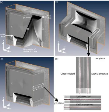
The effectiveness of the drift-correction procedure and resulting quality of the slicing can be analyzed by forming image stacks from both the uncorrected and drift-corrected I-SE images. Figure 4 shows clearly the necessity for the automated drift-correction procedure. The main image in Figure 4a shows the I-SE plan-view image~thexyplane!of the material volume at the start of the slicing process. Overlaid are orthogonal lines through one of the reference crosses indicating the positions from which the xzand yz
[image:4.594.118.476.56.427.2]~this is critical to the spatial resolution of the reconstruction along the slicing direction!. By forming a sum of projection images in the xz plane from the region of the trench headwall, its displacement with each slice can be checked. Doing this confirmed that the slice thickness, 100 nm, was constant throughout the process.
Details of the E-SE Imaging Process
The conditions used for SEM imaging of the cross-section face after each slice were the optimal conditions discussed previously~5 keV, 0.40 nA, 3ms dwell, 16 frames average!. The focus of the electron beam was automatically adjusted to compensate for the slight increase in working distance that occurs as the cross-section face is sequentially milled.
From the observations made during the initial repeated E-SE imaging experiment, it was expected that electrical charging would exert a significant influence upon the imaging during the serial sectioning procedure too. While this was the case, the situation here was improved. The slice milling and imaging procedure inflicts first positively charged ions then negatively charged electrons upon the cross-section face. While the charges are indeed opposite, it would not be expected that they should cancel each other out. During the serial sectioning procedure, it was observed that the level of drift of the E-SE images was small enough that it could be corrected for later in post-processing of the E-SE image stack. Therefore, drift correc-tion of the E-SE images was not performed in order to reduce the overall run time. Again, as for the initial repeated imaging experiment, a problematic linear increase in bright-ness was observed to occur. This resulted in saturation of areas of the E-SE images, obscuring both microstructural and crack features, in the latter part of the serial sectioning sequence. To deal with this, two E-SE images were acquired per slice, the first using the detector amplifier conditions
~contrast and brightness!set at the start of the run and the second utilizing a compensating brightness reduction. The magnitude of the brightness reduction was empiri-cally determined over several sectioning runs and applied as a linear correction with slice number. Figure 5 shows
two electron beam images of the same area of interest:
~a! one taken without brightness correction and ~b! one with. It can be seen that the automated reduction of brightness has avoided obscuration of image features due to saturation.
3-D Reconstruction
After tilt correction, E-SE images were aligned using Avizo, and subsurface crack contours were drawn on each slice using the image analysis software IMOD~Fig. 6a!while the microstructure was reconstructed using Avizo~Fig. 6b!.
In reconstructing the microstructure, two major diffi-culties were encountered that arose from charging effects: a brightness gradient from the top to the bottom of the cross section and shadow effects from the side walls. These two phenomena induce difficulties during segmentation by in-troducing different gray levels within the same phase. Thus, data segmentation by a global threshold value is no longer possible. As only a limited number of filters were available for segmentation in Avizo, a customized script was created in Matlab to overcome this issue. This script used linear filters and two local thresholds to transform the gray level images to binary ones ~with the intergranular phase in white and the grains in black!. Then a filter to remove small objects ~noise! was used, and the binary images obtained were superimposed to the original ones to check the filter-ing process. Binary images were then segmented in Avizo using a global threshold.
Reconstruction of subsurface cracks was manually per-formed on each slice. Individual cracks were identified and tagged, and the crack surface area was calculated by inter-polating between consecutive slices. As the z-projections showed a constant slice thickness of 100 nm, an estimation of the crack surface area was possible and gave a value of 340mm2.
[image:5.594.49.290.57.215.2]The calculations above assume that all cracks observed are resulting from the indentation experiment. However, they do not take into account the fact that FIB sputtering induces changes in residual stress fields. By opening a new free surface, local residual stresses are reduced that leads to an opening or a closing of existing cracks. Moreover, it has Figure 5. Electron beam images taken~a!without and ~b! with
[image:5.594.305.546.58.161.2]brightness correction. 194#124 mm~150#150 DPI!.
Figure 6. a:Reconstruction of cracks underneath a 2 N indent in Syalon 101. Each individual line is a contour from each individual slice, and each color represents a different crack. The surface is in gray. b: Reconstruction of the microstructure. 209 # 91 mm
estimate the percentage of cracks being opened or closed during the FIB process is currently in progress. This will permit the calculation of the true area of cracks opened during indentation, leading to an estimation of the energy dissipated during the cracking process.
CONCLUSIONS
Through developing a highly flexible script platform, we have been able to investigate, by FIB serial sectioning, the subsurface damage induced by indentation in a brittle highly insulating ceramic. As we have described, the variety of effects due to electrical charging posed the greatest diffi-culty for the automated serial sectioning procedure. By overcoming these, reconstruction of the 3D volume under the indent, including both the microstructure and the cracks, was performed allowing visualization of the crack structure and quantification of its surface area.
ACKNOWLEDGMENTS
This work was supported by SFI~Science Foundation Ire-land!. The authors also acknowledge financial support from the European Union under the Framework 6 program un-der a contract for an Integrated Infrastructure Initiative
~Reference 026019 ESTEEM!.
REFER ENCES
Claves, S.R., Bandar, A.R., Misiolek, W.Z. & Michael, J.R.
~2004!. Three-dimensional~3D!reconstruction of AlFeSi inter-metallic particles in 6xxx aluminum alloys using the focused ion beam~FIB!.Microsc Microanal10, 1138–1139.
Elfallagh, F.&Inkson, B.J.~2008!. 3D tomographic analysis of crack morphologies in alumina and glass using FIB micros-copy.J Phys Conf Ser126, 1–4.
Goldstein, J., Newbury, D., Joy, D., Lyman, C., Echlin, P., Lifshin, E., Sawyer, L.&Michael, J.~2003!.Scanning Elec-tron Microscopy and X-ray Microanalysis. New York: Springer. Holzapfel, C., Schaf, W., Marx, M., Vehoff, H.&Mucklich, F.
~2007!. Interaction of cracks with precipitates and grain bound-aries: Understanding crack growth mechanisms through fo-cused ion beam tomography.Scripta Mater56, 697–700.
Kammer, D., Mendoza, R., Barnett, S.A. & Voorhees, P.W.
~2005!. The three-dimensional microstructure of materials: Mea-surement and analysis.Microsc Microanal11, 72–73.
Kato, M., Ito, T., Aoyama, Y., Sawa, K., Kaneko, T., Kawase, N.& Jinnai, H.~2007!. Three-dimensional structural analysis of a block copolymer by scanning electron microscopy combined with a focused ion beam.J Polymer Sci B: Polymer Phys45, 677–683. Kremer, J.R., Mastronarde, D.N. & McIntosh, J.R. ~1996!.
Computer visualization of three-dimensional image data using IMOD.J Struct Biol116, 71–76.
Matthijs De Winter, D.A., Schneijdenberg, C.T.W.M., Leb-bink, M.N., Lich, B., Verkleij, A.J., Drury, M.R.&Humbel, B.M.~2009!. Tomography of insulating biological and geologi-cal materials using focused ion beam ~FIB! sectioning and low-kV BSE imaging.J Microsc233, 372–383.
McGrouther, D.&Munroe, P.R.~2007!. Imaging and analysis of 3-D structure using a dual beam FIB.Microsc Res Techniq70, 186–194.
Schaffer, M., Wagner, J., Schaffer, B., Schmied, M.& Mul-ders, H.~2007!. Automated three-dimensional X-ray analysis using a dual-beam FIB.Ultramicroscopy107, 587–597. Steer, T.J., Möbus, G., Kraft, O., Wagner, T. & Inkson, B.J.
~2001!. 3D FIB and AFM mapping of nanoindentation zones. Mater Res Soc Symp Proc649, 3.3.1–3.3.6.
Steer, T.J., Möbus, G., Kraft, O., Wagner, T.&Inkson, B.J.~2002!. 3-D-focused ion beam mapping of nanoindentation zones in a Cu-Ti multilayered coating.Thin Solid Films413, 147–154. Uchic, M.D., Groeber, M.A., Dimiduk, D.M.& Simmons, J.P.
~2006!. 3D microstructural characterization of nickel superal-loys via serial-sectioning using a dual beam FIB-SEM.Scripta Mater55, 23–28.
Williams, R., Bhattacharyya, D., Viswanathan, G.B., Baner-jee, R.&Fraser, H.L.~2004!. Application of FIB-tomography to the study of microstructures in titanium alloys. Microsc Microanal10~S2!, 1178–1179~CD-ROM!.
Williams, R., Uchic, M., Dimiduk, D. & Fraser, H.L.~2006!. Three dimensional reconstruction of alpha laths in alpha/beta titanium alloys by serial sectioning with a FEI NOVA 600. Microsc Microanal12~S2!, 1234–1235~CD-ROM!.